Part Number: LAUNCHXL-F28069M
Other Parts Discussed in Thread: C2000WARE
Tool/software: Code Composer Studio
Hello all,
I have created a program which is communicating with an E²PROM via I²C and PC via SCI. When Launchxl is first energized, it reads from E²PROM and writes the values to my parameters. Then with my pc interface, I can read these values or change these (write to Launchxl).
But this only works on debug mode perfectly.
When I does not start debug mode via ccs and only conect Launchxl to pc's usb, as I understand, sci is not working. But other functions are ok. Eeprom is answering the attend, launchxl gets the retentive values, I can even trigger ePWM.
Sci signal is being received but Launchxl does not understand the command.
I cannot always start the debug mode. As I understand, my FLASH map is not included sci. I could not understand that part good enough actually.
My FLASH map is given below.
MEMORY
{
PAGE 0 :   /* Program Memory */
           /* Memory (RAM/FLASH/OTP) blocks can be moved to PAGE1 for data allocation */
/*
   RAML0       : origin = 0x008000, length = 0x000800
   RAML1       : origin = 0x008800, length = 0x000400
*/

   OTP         : origin = 0x3D7800, length = 0x000400     /* on-chip OTP */

	FLASH		: origin = 0x3D8000, length = 0x018000
	RAM			: origin = 0x008000, length = 0x00C000

/*
   FLASHH      : origin = 0x3D8000, length = 0x004000
   FLASHG      : origin = 0x3DC000, length = 0x004000
   FLASHF      : origin = 0x3E0000, length = 0x004000
   FLASHE      : origin = 0x3E4000, length = 0x004000
   FLASHD      : origin = 0x3E8000, length = 0x004000
   FLASHC      : origin = 0x3EC000, length = 0x004000
*/

   FLASHA      : origin = 0x3F4000, length = 0x003F80     /* on-chip FLASH */
   CSM_RSVD    : origin = 0x3F7F80, length = 0x000076     /* Part of FLASHA.  Program with all 0x0000 when CSM is in use. */
   BEGIN       : origin = 0x3F7FF6, length = 0x000002     /* Part of FLASHA.  Used for "boot to Flash" bootloader mode. */
   CSM_PWL_P0  : origin = 0x3F7FF8, length = 0x000008     /* Part of FLASHA.  CSM password locations in FLASHA */

   FPUTABLES   : origin = 0x3FD860, length = 0x0006A0	  /* FPU Tables in Boot ROM */
   IQTABLES    : origin = 0x3FDF00, length = 0x000B50     /* IQ Math Tables in Boot ROM */
   IQTABLES2   : origin = 0x3FEA50, length = 0x00008C     /* IQ Math Tables in Boot ROM */
   IQTABLES3   : origin = 0x3FEADC, length = 0x0000AA	  /* IQ Math Tables in Boot ROM */

   ROM         : origin = 0x3FF3B0, length = 0x000C10     /* Boot ROM */
   RESET       : origin = 0x3FFFC0, length = 0x000002     /* part of boot ROM  */
   VECTORS     : origin = 0x3FFFC2, length = 0x00003E     /* part of boot ROM  */

PAGE 1 :   /* Data Memory */
           /* Memory (RAM/FLASH/OTP) blocks can be moved to PAGE0 for program allocation */
           /* Registers remain on PAGE1                                                  */

	SYSRAM			: origin = 0x000000, length = 0x000800

/*
   BOOT_RSVD   : origin = 0x000000, length = 0x000050
   RAMM0       : origin = 0x000050, length = 0x0003B0
   RAMM1       : origin = 0x000400, length = 0x000400
*/


/*
   RAML2       : origin = 0x008C00, length = 0x000400
   RAML3       : origin = 0x009000, length = 0x001000
   RAML4       : origin = 0x00A000, length = 0x002000
   RAML5       : origin = 0x00C000, length = 0x002000
   RAML6       : origin = 0x00E000, length = 0x002000
   RAML7       : origin = 0x010000, length = 0x002000
   RAML8       : origin = 0x012000, length = 0x002000
*/

   USB_RAM     : origin = 0x040000, length = 0x000800     /* USB RAM		  */
   FLASHB      : origin = 0x3F0000, length = 0x004000     /* on-chip FLASH */
}

/* Allocate sections to memory blocks.
   Note:
         codestart user defined section in DSP28_CodeStartBranch.asm used to redirect code
                   execution when booting to flash
         ramfuncs  user defined section to store functions that will be copied from Flash into RAM
*/


SECTIONS
{
   /* Allocate program areas: */
   .cinit              : > FLASH,     	PAGE = 0
   .pinit              : > FLASH,     	PAGE = 0
   .text               : > FLASH,     	PAGE = 0
   codestart           : > BEGIN,      	PAGE = 0
/*
   ramfuncs            : LOAD = FLASHD,
                         RUN = RAML0,
                         LOAD_START(_RamfuncsLoadStart),
                         LOAD_END(_RamfuncsLoadEnd),
                         RUN_START(_RamfuncsRunStart),
						 LOAD_SIZE(_RamfuncsLoadSize),
                         PAGE = 0
*/
   csmpasswds          : > CSM_PWL_P0, PAGE = 0
   csm_rsvd            : > CSM_RSVD,   PAGE = 0

   /* Allocate uninitalized data sections: */
   .stack              : > SYSRAM,      PAGE = 1
   .ebss               : > RAM,      	PAGE = 0
   .esysmem            : > RAM,      	PAGE = 0

   /* Initalized sections to go in Flash */
   /* For SDFlash to program these, they must be allocated to page 0 */
   .econst             : > FLASH,     PAGE = 0
   .switch             : > FLASH,     PAGE = 0

   GROUP
    {
    	.TI.ramfunc
    	ramfuncs{
    	rts2800_fpu32.lib<fs_div.obj>(.text)
    	}
    	dclfuncs
    }    LOAD = FLASH,
         RUN = RAM,
         PAGE = 0,
         TABLE(BINIT)

   .binit : palign=0x8, fill=0xffff > FLASH

   /* Allocate IQ math areas: */
   IQmath              : > FLASH,     PAGE = 0            /* Math Code */
   IQmathTables        : > IQTABLES,   PAGE = 0, TYPE = NOLOAD

   /* Allocate FPU math areas: */
   FPUmathTables       : > FPUTABLES,  PAGE = 0, TYPE = NOLOAD

   /*
   DMARAML5	           : > RAML5,      PAGE = 1
   DMARAML6	           : > RAML6,      PAGE = 1
   DMARAML7	           : > RAML7,      PAGE = 1
   DMARAML8	           : > RAML8,      PAGE = 1
   */

  /* Uncomment the section below if calling the IQNexp() or IQexp()
      functions from the IQMath.lib library in order to utilize the
      relevant IQ Math table in Boot ROM (This saves space and Boot ROM
      is 1 wait-state). If this section is not uncommented, IQmathTables2
      will be loaded into other memory (SARAM, Flash, etc.) and will take
      up space, but 0 wait-state is possible.
   */
   /*
   IQmathTables2    : > IQTABLES2, PAGE = 0, TYPE = NOLOAD
   {

              IQmath.lib<IQNexpTable.obj> (IQmathTablesRam)

   }
   */
    /* Uncomment the section below if calling the IQNasin() or IQasin()
       functions from the IQMath.lib library in order to utilize the
       relevant IQ Math table in Boot ROM (This saves space and Boot ROM
       is 1 wait-state). If this section is not uncommented, IQmathTables2
       will be loaded into other memory (SARAM, Flash, etc.) and will take
       up space, but 0 wait-state is possible.
    */
    /*
    IQmathTables3    : > IQTABLES3, PAGE = 0, TYPE = NOLOAD
    {

               IQmath.lib<IQNasinTable.obj> (IQmathTablesRam)

    }
    */

   /* .reset is a standard section used by the compiler.  It contains the */
   /* the address of the start of _c_int00 for C Code.   /*
   /* When using the boot ROM this section and the CPU vector */
   /* table is not needed.  Thus the default type is set here to  */
   /* DSECT  */
   .reset              : > RESET,      PAGE = 0, TYPE = DSECT
   vectors             : > VECTORS,    PAGE = 0, TYPE = DSECT


}
It is a modified version of F28069.cmd. The normal F28069.cmd does not work properly for me but this one was perfect except sci.
I have checked Example_2806xFlash, Example_2806xFlashProgramming, f28069_sci_flash_kernel but could understand their purpuse or if they are related.
What should I do exactly? If I should give more details, lead me, please.
Thank you.
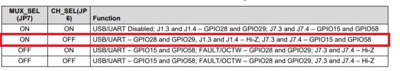
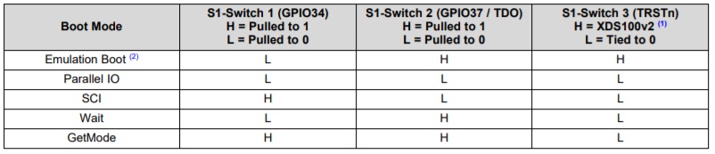
P.S : S1 DIP switches are all 1 (H) on LaunchXL-F28069M. JP6 is not connected and JP7 is connected. I have worked that way until now.