This thread has been locked.

If you have a related question, please click the "Ask a related question" button in the top right corner. The newly created question will be automatically linked to this question.

TMS320F28069: Implementing high-speed UART with McBSP

Part Number: TMS320F28069
Other Parts Discussed in Thread: C2000WARE, MOTORWARE

Hello,

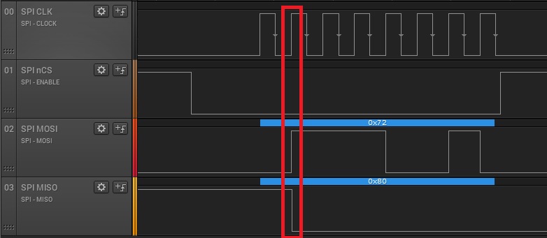
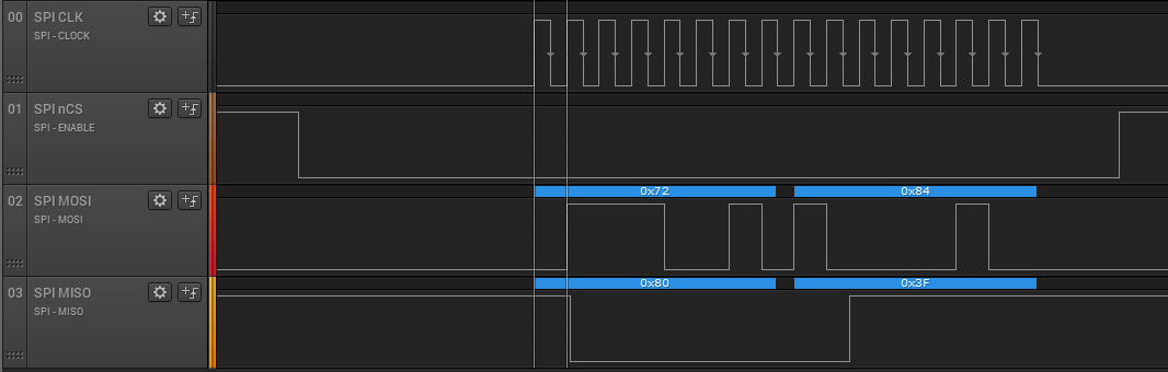
We were able to implement a high-speed (3.75 Mbit/s) UART using the SCI port of the C2000 (each byte received/sent generates an interrupt). However, since we are running an InstaSPIN FOC controller at 10KHz in parallel to this high-speed UART, the code of the main loop is always interrupted by UART reception/transmission interrupts (16 bytes received/12 bytes sent every millisecond) and by FOC controller interrupts. This behavior creates non-negligible delays on code running outside interrupts.

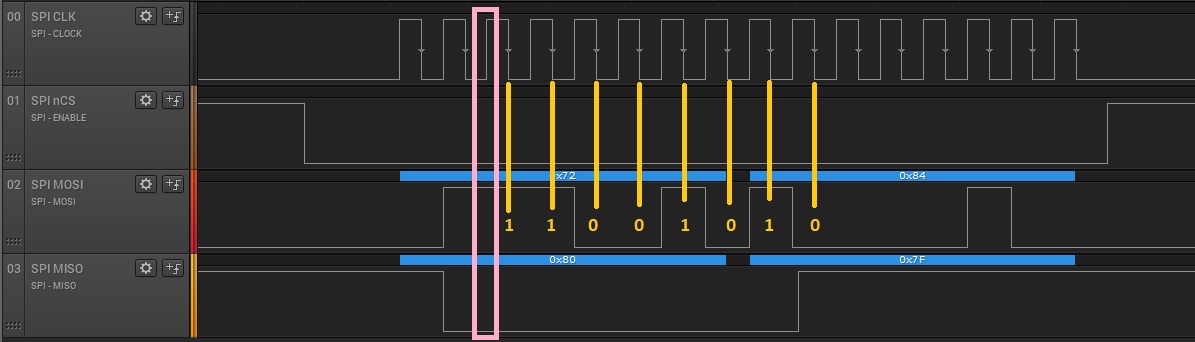
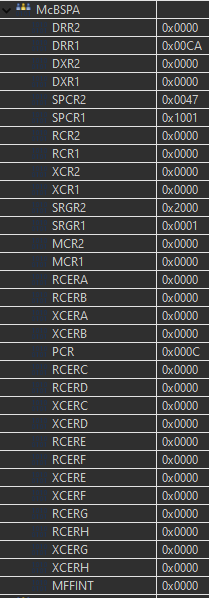
Our idea to solve the above issue would be to implement this UART using the McBSP port with DMA support to give more processing time to the main code. It is important to note that the UART has the highest priority in our system and transfers must be done each millisecond.

Before starting this implementation, we need you to help us on the following questions:

  • Is it possible to implement a high-speed UART (target = 3.75Mbit/s) using McBSP and DMA?
  • If yes, do you have any examples that can speed up the development?
  • If no:
    • What are the limitations?
    • Is there any other way to improve the current UART solution and reduce processing time?

Regards,
Johann

  • Johann,

    If you have gotten the 3.75Mbit/s with CPU and McBSP, then I definitely think the DMA/McBSP will be capable of this.  There is an example of the DMA/McBSP in C2000Ware, here is the online version although you can also find this in a local install if that is preferable.

    Let me know if you have further questions regarding the example or implementing this in your system.

    Best,
    Matthew 

  • Hello Matthew,

    We did not use the McBSP at all. At the moment, we hare reaching 3.75 Mbit/s using SCI and RX/TX interrupts.

    So can you please confirm that we can obtain such high-speed with McBSP + DMA?

    Thank you for your help.

    Regards,
    Johann

  • Johan,

    I found a supporting E2E post here: https://e2e.ti.com/support/microcontrollers/c2000/f/171/t/787004?tisearch=e2e-sitesearch&keymatch=Single%20Phase%20UPS but will summarize the different parameters that are in play.  

    Based on the below your data rate of 3.75Mbps using McBSP as SPI and reading with the DMA should be possible:

    1)Any comm on this device is limited by the max GPIO toggling rate, which is 25MHz, so we are OK there

    2)For the McBSP the master clock rate is defined as 2 * CLKG, where CLKG is the clock source for the McBSP/(1+ CLKGDV).  For SPI mode you are going to use the LSPCLK, which can be as fast as the CPU clock.  Since LSPCLK feeds other periperhals I'll need you to comment on that rate, and if it is dictated by antother peripheral.  At 3.75MBps we should have ample headroom we just need to substitute whatever CLKGDV makes sense based on LSPCLK

    3)Finally, McBSP is located on peripheral frame 3(SPI was on PF2) and both have 0WS writes, but 2 WS reads.  Again, since the DMA and LSP clock is running at full clock rate of 90MHz(assuming the MCU clock is 90MHz) our read rate from this frame would be capped at 30MHz, which is more than enough for your data rate.  If your LSPclock is lower we can work out the math on that as well but we should be able to do this.

    4)Implementation, as I mentioned there are some examples in C2000Ware, but the DMA is fully capable of handling the McBSP data stream independent of the CPU.  That is there is input into the DMA for the McBSP transmit and receive signals, so that it can capture the data.  You can then choose when the DMA should trigger its ISR to the main CPU for whatever data processing you need to do on any amount of data, that is one or many receives.

    While there are DMA examples in C2000Ware, if you would like some specific recommendations for configuration based on what you need to do I'll be happy to give some help on that as well.

    Please let me know if you have further questions.

    Best,
    Matthew

  • Dear Matthew,

    Thank you for your detailed inputs.

    However, you're talking about SPI but in our case, we want to implement UART over McBSP.

    Are your points applicable to UART through McBSP as well? If yes, is there any differences regarding SPI in your points above?

    Regards,
    Johann

  • I don't think you can implement UART with McBSP. McBSP is in it's basis synchronous port and requires clock input when receiving.

    For higher transmission speeds you'll have to change the transmission bus. And with 28069 SPI port is the most sensible one, as you can use DMA with McBSP and McBSP in SPI mode.

  • Johann,

    Firstly, I want to apologize on my error in the above response; since we have a native SPI mode in the McBSP and we often get that question due to the DMA and I mis-read your post.

    I'm looking to see if there is applicablilty of an app note we have inside TI that was implemented on another TI processor.  My experience is that the McBSP logic is the same across our devices; but I want to make certain of this.

    For the sake of time the app note is here if you want to take a look  http://www.ti.com/lit/spra633 .

    In a nutshell the limiting factor would be that whatever McBSP/SPI mode data rate we had would need to be divided down by 16, since we will use 1 SPI slot for one bit of a 16 bit transfer.  There is some amount of CPU overhead, but I think we can take care of this in the DMA.

    Best,

    Matthew

  • Hello everyone,

    for some reasons the link above does not work, find the document here: 

    Best regards,

    Ambroise

  • Hello Matthew,

    Finally we will go for SPI over McBSP using DMA since it makes more sense as the SPI seems to be more "native" compared to the UART.

    We are thus implementing a slave SPI.

    I've integrated McBSP in my code based on Example_2806xMcBSP_SPI_DLB and Example_2806xMcBSP_DLB_DMA but using my own libraries since my code is based on a C2000 Motorware project.

    I tried to make it work the whole day but I was not able to communicate at all with a master. The master tries to send 18 bytes to the slave (McBSP) but the McBSP seems to only react at the first clock rising edge. After that, the MISO line remains at a logic low level. I have checked the McBSP and DMA registers to see if any status occurs during and after the transfer but all registers remain the same (no bit change).

    On the master side, we have implemented a feature that release nCS pin after 4 bytes during more that 2 bits to fulfill McBSP requirement.

    Here is the code I developed.

    GPIO configuration (GPIOs used are 50, 51, 52 and 53) and are set to McBSP function + asynchronous qualification.

      gpio = (GPIO_Number_e)HAL_GPIO_McBspMdxA;
      GPIO_setMode(obj->gpioHandle, gpio, GPIO_50_Mode_MDXA);
      GPIO_setQualification(obj->gpioHandle, gpio, GPIO_Qual_ASync);
    
      gpio = (GPIO_Number_e)HAL_GPIO_McBspMdrA;
      GPIO_setMode(obj->gpioHandle, gpio, GPIO_51_Mode_MDRA);
      GPIO_setQualification(obj->gpioHandle, gpio, GPIO_Qual_ASync);
    
      gpio = (GPIO_Number_e)HAL_GPIO_McBspMclkxA;
      GPIO_setMode(obj->gpioHandle, gpio, GPIO_52_Mode_MCLKXA);
      GPIO_setQualification(obj->gpioHandle, gpio, GPIO_Qual_ASync);
    
      gpio = (GPIO_Number_e)HAL_GPIO_McBspMfsxA;
      GPIO_setMode(obj->gpioHandle, gpio, GPIO_53_Mode_MFSXA);
      GPIO_setQualification(obj->gpioHandle, gpio, GPIO_Qual_ASync);

     McBSP configuration

    void
    HAL_setupMcBspA (HAL_Handle handle)
    {
      HAL_Obj *obj = (HAL_Obj *)handle;
      McBSP_obj *mcbsp = (McBSP_obj *)obj->mcbspAHandle;
    
      mcbsp->SPCR2 = 0x0000U;
      mcbsp->SPCR1 = 0x0000U;
    
      // Step 1: place the transmitter and receiver in reset.
      // ----------------------------------------------------------
      mcbsp->SPCR2 &= ~MCBSP_SPCR2_XRST;
      mcbsp->SPCR1 &= ~MCBSP_SPCR1_RRST;
      // Step 2: place the sample rate generator in reset.
      // ----------------------------------------------------------
      mcbsp->SPCR2 &= ~MCBSP_SPCR2_GRST;
      // Step 3: program registers that affect SPI operation.
      // ----------------------------------------------------------
      mcbsp->SPCR1 &= ~MCBSP_SPCR1_CLKSTP;
      mcbsp->SPCR1 |= (2 << MCBSP_SPCR1_CLKSTP_POS);  // Clock stop mode, without clock delay.
    
      // SPI mode 0 selection (low inactive state, McBSP transmit data on
      // the rising edge of SCLK and receives data on the falling edge.
      mcbsp->PCR &= ~MCBSP_PCR_CLKXP;
      mcbsp->PCR &= ~MCBSP_PCR_CLKRP;
    
      mcbsp->PCR &= ~MCBSP_PCR_CLKXM;  // Clock is received on the MCLKX pin.
    
      // Set the single-phase transmit/receive frame.
      mcbsp->XCR2 &= ~MCBSP_XCR2_XPHASE;
      mcbsp->RCR2 &= ~MCBSP_RCR2_RPHASE;
    
      // Set the transmit and receive frame length of 1 serial word.
      mcbsp->XCR1 &= ~MCBSP_XCR1_XFRLEN1;
      mcbsp->RCR1 &= ~MCBSP_RCR1_RFRLEN1;
    
      // Set the transmit and receive packet length to 32 bits.
      mcbsp->XCR1 |= (0x05 << MCBSP_XCR1_XWDLEN1_POS);
      mcbsp->RCR1 |= (0x05 << MCBSP_RCR1_RWDLEN1_POS);
    
      // Select LSPCLK as input clock for the sample rate generator.
      mcbsp->PCR &= ~MCBSP_PCR_SCLKME;
      mcbsp->SRGR2 |= MCBSP_SRGR2_CLKSM;
    
      // Divide-down the LSPCLK by 2 (maximum authorized frequency for McBSP).
      mcbsp->SRGR1 &= ~MCBSP_SRGR1_CLKGDV;
      mcbsp->SRGR1 |= (1 << MCBSP_SRGR1_CLKGDV_POS);
    
      // FSX pin is an input pin and used for chip select.
      mcbsp->PCR &= ~MCBSP_PCR_FSXM;
    
      // FSX pin is active low.
      mcbsp->PCR |= MCBSP_PCR_FSXP;
    
      // SPI slave operation requires fields XDATDLY and RDATDLY to be set to 0.
      mcbsp->XCR2 &= ~MCBSP_XCR2_XDATDLY;
      mcbsp->RCR2 &= ~MCBSP_RCR2_RDATDLY;
    
      // Step 4: enable the sample rate generator.
      // ----------------------------------------------------------
      mcbsp->SPCR2 |= MCBSP_SPCR2_GRST;
    
      HAL_usDelay(100);
    
      // Step 5: enable the transmitter and the receiver.
      // ----------------------------------------------------------
      mcbsp->SPCR2 |= MCBSP_SPCR2_XRST;
      mcbsp->SPCR1 |= MCBSP_SPCR1_RRST;
    
      HAL_usDelay(100);
    }

    DMA configuration

    #pragma DATA_SECTION(m_spiDmaTestRxBuf, "DMARAML5")
    #pragma DATA_SECTION(m_spiDmaTestTxBuf, "DMARAML5")
    uint16_t m_spiDmaTestRxBuf[9] = { 0U, 0U, 0U, 0U, 0U, 0U, 0U, 0U, 0U };
    uint16_t m_spiDmaTestTxBuf[9] = { 0xFEED, 0xDEAD, 0xBEEF, 0xF00D, 0xCAFE, 0x1234, 0x5678, 0xFACE, 0xB00C };
    
    void
    HAL_setupMcBspADma (HAL_Handle handle)
    {
      HAL_Obj *obj = (HAL_Obj *)handle;
      DMA_obj *dma = (DMA_obj *)obj->dmaHandle;
    
      ENABLE_PROTECTED_REGISTER_WRITE_MODE;
    
      dma->DMACTRL |= (1 << 0);
      asm(" nop");
    
      // Channel 1: McBSPA receive
      // ----------------------------------------------------------
    
      dma->CH1.BURST_SIZE = 1U;       // 2 16-bit word per burst
      dma->CH1.SRC_BURST_STEP = 1U;   // increment 1 16-bit addr. between words
      dma->CH1.DST_BURST_STEP = 1U;   // increment 1 16-bit addr. between words
      dma->CH1.TRANSFER_SIZE = 9U;    // Interrupt every 9 bursts (= 18 bytes).
    
      dma->CH1.SRC_TRANSFER_STEP = 0xFFFFU; // Decrement back to McBSP DRR2 register.
      dma->CH1.DST_TRANSFER_STEP = 1U; // Move to next word in buffer after each word in a burst.
    
      dma->CH1.SRC_ADDR_SHADOW = (uint32_t)&obj->mcbspAHandle->DRR2;
      dma->CH1.SRC_BEG_ADDR_SHADOW = (uint32_t)&obj->mcbspAHandle->DRR2; // TODO (S) : not needed - to be checked.
      dma->CH1.DST_ADDR_SHADOW = (uint32_t)&m_spiDmaTestRxBuf[0];
      dma->CH1.DST_BEG_ADDR_SHADOW = (uint32_t)&m_spiDmaTestRxBuf[0]; // TODO (S) : not needed - to be checked.
    
      // Clear sync error flag
      dma->CH1.CONTROL |= (1U << 7);
    
      // Set to maximum to avoid any source/destination wrap.
      dma->CH1.SRC_WRAP_SIZE = 0xFFFFU;
      dma->CH1.DST_WRAP_SIZE = 0xFFFFU;
    
      dma->CH1.MODE |= (1U << 15); // Enable channel interrupt.
      dma->CH1.MODE |= (1U << 9); // Generate interrupt at end of transfer.
      dma->CH1.MODE |= (1U << 8); // Enable peripheral interrupt event.
    
      dma->CH1.MODE |= (15U << 0); // DMA interrupt source: MREVTA (McBSP reception).
    
      dma->CH1.CONTROL |= (1U << 4); // Clear any spurious interrupt flags.
    
      // Channel 2: McBSPA transmit
      // ----------------------------------------------------------
    
      dma->CH2.BURST_SIZE = 1U;       // 2 16-bit word per burst
      dma->CH2.SRC_BURST_STEP = 1U;   // increment 1 16-bit addr. between words
      dma->CH2.DST_BURST_STEP = 1U;   // increment 1 16-bit addr. between words
      dma->CH2.TRANSFER_SIZE = 9U;    // Interrupt every 9 bursts (= 18 bytes).
    
      dma->CH2.SRC_TRANSFER_STEP = 1U; // Move to next word in buffer after each word in a burst.
      dma->CH2.DST_TRANSFER_STEP = 0xFFFFU; // Decrement back to McBSP DRR2 register.
    
      dma->CH2.SRC_ADDR_SHADOW = (uint32_t)&m_spiDmaTestTxBuf[0];
      dma->CH2.SRC_BEG_ADDR_SHADOW = (uint32_t)&m_spiDmaTestTxBuf[0]; // TODO (S) : not needed - to be checked.
      dma->CH2.DST_ADDR_SHADOW = (uint32_t)&obj->mcbspAHandle->DXR2;
      dma->CH2.DST_BEG_ADDR_SHADOW = (uint32_t)&obj->mcbspAHandle->DXR2; // TODO (S) : not needed - to be checked.
    
      // Clear sync error flag
      dma->CH2.CONTROL |= (1U << 7);
    
      // Set to maximum to avoid any source/destination wrap.
      dma->CH2.SRC_WRAP_SIZE = 0xFFFFU;
      dma->CH2.DST_WRAP_SIZE = 0xFFFFU;
    
      dma->CH2.MODE |= (1U << 15); // Enable channel interrupt.
      dma->CH2.MODE |= (1U << 9); // Generate interrupt at end of transfer.
      dma->CH2.MODE |= (1U << 8); // Enable peripheral interrupt event.
    
      dma->CH2.MODE |= (14U << 0); // DMA interrupt source: MXEVTA (McBSP transmission).
    
      dma->CH2.CONTROL |= (1U << 4); // Clear any spurious interrupt flags.
    
      DISABLE_PROTECTED_REGISTER_WRITE_MODE;
    }

    Other important information:

    • LSPCLK is equal to SYSCLKOUT (90 MHz)
    • DMA is configured and started (both channels) before the McBSP is configured.
    • DMA interrupts (for each channel) are enabled after the McBSP is configured using the following code (and their handlers are correctly set):
    void
    HAL_enableMcBspADmaInt (HAL_Handle handle)
    {
      HAL_Obj *obj = (HAL_Obj *)handle;
    
      PIE_enableInt(obj->pieHandle, PIE_GroupNumber_7, PIE_InterruptSource_DMA_CH1);
      PIE_enableInt(obj->pieHandle, PIE_GroupNumber_7, PIE_InterruptSource_DMA_CH2);
    
      CPU_enableInt(obj->cpuHandle, CPU_IntNumber_7);
    }
    • McBSP and DMA peripherals are clocked.
    • We have tried with clock frequencies from 6MHz down to 400kHz: same problem.
    • I was able to make the McBSP SPI loopback example with my code (configurations modified).

    Q1: Could you please review the McBSP and DMA configuration?
    Q2: Do you see anything else that is missing or could be problematic in our approach?

    Here are the minimal drivers compatible with Motorware for McBSP and DMA as well as the CLK driver updated with DMA and McBSP peripherals clocks enabling functions:

    /cfs-file/__key/communityserver-discussions-components-files/171/mcbsp.h

    /cfs-file/__key/communityserver-discussions-components-files/171/mcbsp.c

    /cfs-file/__key/communityserver-discussions-components-files/171/dma.h

    /cfs-file/__key/communityserver-discussions-components-files/171/dma.c

    /cfs-file/__key/communityserver-discussions-components-files/171/clk.h

    /cfs-file/__key/communityserver-discussions-components-files/171/clk.c

    I added these two lines in the HAL_Obj structure (in hal_obj.h file):

      MCBSP_Handle mcbspAHandle;
      DMA_Handle dmaHandle;

    I added these two lines at the end of HAL_init function (in hal.c file):

      obj->mcbspAHandle = mcbsp_init((void*)MCBSPA_BASE_ADDR, sizeof(McBSP_obj));
      obj->dmaHandle = dma_init((void*)DMA_BASE_ADDR, sizeof(DMA_obj));

    I added these two lines at the end of HAL_setupPeripheralClks function (in hal.c file):

      CLK_enableMcbspAClock(obj->clkHandle);
      CLK_enableDmaClock(obj->clkHandle);


    Regards,
    Johann

  • Hello,

    Here is an update.

    We tried sending and receiving one byte with the McBSP as a SPI slave without DMA, but we haven't been able to make it work for now.

    The master sends the byte 0x72 with a clock frequency of about 200kHz (for test purpose only) in SPI mode 0 (CPOL = 0, CPHA = 1). The slave should answer in full-duplex with byte 0x00 (McBSP is in the mode defined by CLKSTP = 10b, CLKXP = 0, CLKRP = 0).

    The McBSP does not receive the byte. Indeed, it seems that some bits are missed based on the plot below. The McBSP begin to transmit via MISO only at the second clock rising edge (highlighted in red).

    We tried to send two bytes instead (0x72 then 0x84) in order to confirm our assumption. In that case, byte 0xCA is received in register DRR1 which means that, for McBSP, the reading starts with the 3rd clock falling edge (highlighted in pink). This confirms our doubts regarding the delay. The plot is shown below.

    The McBSP configuration is the same as described in the previous post but with the difference that RWDLEN1 and XWDLEN1 are now 0 (8-bit). Here are the values in the McBSP registers (FYI):

    Q3: Where does this delay come from? We spent the whole day trying to figure out how to solve this issue but we are running out of ideas. Please give us your support.

    Q4: Our LSPCLK is 90MHz. Is that OK for a CLKGDV of 1?

    Q5: + see questions Q1 and Q2 in previous post.

  • Johann,

    Just want to give an update letting you know I'm still reviewing the code, its taking me some time to parse through both the Motorware + McBSP settings.  

    Can you comment on the LSPCLK rate you have set for the overall system?  While LSPCLK can equal SYSCLK(90MHz max), there is a 20MHz McBSP clock restriction according to the datasheet.  If LSPCLK = 90MHz then CLKG = 45MHz which would be out of spec.  You would need make CLKGDV = 4 to get 18MHz CLKG to meet the spec(3 would give 22.5MHz which is still above spec).

    I'll continue to parse through the code, I agree that we should focus on the McBSP/SPI code for now and can add the DMA code in once we get the comms up a and working.

    Best,

    Matthew

  • Hello Matthew,

    Can you comment on the LSPCLK rate you have set for the overall system?

    As already mentioned in my previous posts, the actual LSPCLK rate is 90 MHz (= SYSCLKOUT).

    While LSPCLK can equal SYSCLK(90MHz max), there is a 20MHz McBSP clock restriction according to the datasheet.  If LSPCLK = 90MHz then CLKG = 45MHz which would be out of spec.  You would need make CLKGDV = 4 to get 18MHz CLKG to meet the spec(3 would give 22.5MHz which is still above spec).

    We have seen this limitation and already tried to increase CLKGDV above 4 to have a CLKG below 20MHz. But this didn't solve the problem.

    Anyway, we have tried your recommendation (CLKGDV = 4) with the SPI master clocking at 750kHz. The problem is still there.

    What is really strange is that the McBSP SPI slave prepares data on MISO only after the first SPI clock instead of directly preparing the data when it detects the assertion of nCS pin (as it is usually done on other ICs).

    Q: Where does this "1 clock delay" comes from (XDATADLY and RDATADLY are 0)?

    Q: Is it possible that there is an undocumented limitation in the McBSP that can lead to this kind of behavior?

    Please understand that we need to solve this ASAP since this is a blocking point on our side and we are currently running out of ideas.

    Regards,
    Johann

  • Agree that from the documenatation we should not be seeing a delay.

    Looking at the PCR register, from your previous post it has a value of 0x0008.  I think this should be either 0x0208(to drive the MCLKX pin) as the SPI master  and recieve clock is just taken internally, or as 0x0308 to additionally take the receive clock from the MCLKR pin if we need to factor in any delay from the path.  I'm assuming that the SPI clock in this instance is generated from the F2806x as the master so if the line/slave delay on the other end is not too much 0x0208 should work.

    Best,

    Matthew

  • Based on the documentation, since the F28069 is in our case a SPI slave, CLKXM (bit 9 of PCR) must be equal to 0 (as we did until now).

    Therefore, I clearly don't get your point of setting PCR with 0x0208 or 0x0308 since it means that CLKXM will be set to 1 (for SPI master only).

    We are trying to make the C2000 behaves as a SPI slave via McBSP, not an SPI master...

  • Johann,

    You are correct, I was getting SPI Slave X-mit crossed with the Master/Slave setting.  Both these bits should be cleared, and that is correct in your code.

    Based on some more investigation I think we are bumping up against a timing/speed issue that is compounded by some of the wording in the datasheet, specifically the comment on the 20MHz limitation based on the GPIO max toggle frequency.

    While that limit is true, in this case I beleive it only applies to the incoming signal on CLKX that comes from the system SPI master.  The McBSP logic, itself, only has a restriction to be 1/2 of SYSCLK.  So, if LSPCLK is already /2 then we can set CLKGDV =0; or if LSPCLK = SYSCLK we just need to set CLKGDV = 1.  That max for a 90MHz CPU clock would be 45MHz.

    For SPI Slave mode this will be particularly important since the internal clock will gate how fast we can sample the master clock on CLKX pin.  There is a restriction wrt this aspect, that the maximum input clock the internal logic can detect/sync to is 8 CLKG periods.  In this case if we have 45MHz CLKG we have to limit the SPI master/input clock to 45/8 or 5.625MHz.  I don't beleive this is a problem from your earlier plots in itself, but when I asked you to  slowed down the CLKG(internal McBSP clock) this was potentially making matters worse since we were loosing sampling resolution and potentially violating the above.

    I also found a note on the GSYNC bit(bit 15 in SRGR2 register) for SPI Slave mode we need to set this to a "1" to synchronize the CLKG to the CLKX signal.  This bit is currently cleared in the setup screen shot you sent earlier.

    The other point I found was the polarity for the transmit and receive clocks.  Right now I beleive they are both set to rising edge polarity(CLKXP and CLKRP =0).  The documentation is not crystal clear on this, but I think in the case of SPI slave we should keep CLKRP =0, but switch CLKXP =1 to give a half cycle of delay to when the C28x SPI Slave will transmit its data back to the master.  

    Let's try all of the above, and see if it resolves the delay you are seeing on both the receive (causing message errors) and transmit.

    Best,
    Matthew

  • Hello Matthew,

    Since time is critical on this project and since we were not able to make McBSP work as a SPI slave, we configured it as a SPI master instead and were able to make it work with DMA in only one day.

    Since this solution seems to work well, we will keep it for the moment and put aside the SPI slave solution.

    I have now a question regarding how to efficiently start DMA transfers using McBSP SPI at regular intervals.

    Indeed, in our system, we starting DMA transfers of 5 bursts of 4 bytes every 1ms. In order to do that, we do the following process each 1ms to start a transfer:

    1. Stop McBSP.
        mcbsp->SPCR2 &= ~(1U << 7);
        mcbsp->SPCR2 &= ~MCBSP_SPCR2_XRST;
        mcbsp->SPCR1 &= ~MCBSP_SPCR1_RRST;
        mcbsp->SPCR2 &= ~MCBSP_SPCR2_GRST;
    2. Setup McBSP DMA transfer.
      ENABLE_PROTECTED_REGISTER_WRITE_MODE;
      
        dma->DMACTRL |= (1 << 0);
        asm(" nop");
      
        // Channel 1: McBSPA transmit
        // ----------------------------------------------------------
      
        dma->CH1.BURST_SIZE = 1U;       // 2 16-bit word per burst
        dma->CH1.SRC_BURST_STEP = 1;   // increment 1 16-bit addr. between words
        dma->CH1.DST_BURST_STEP = 1;   // increment 1 16-bit addr. between words
        dma->CH1.TRANSFER_SIZE = 4U;    // Interrupt every (4 + 1) bursts (= 20 bytes).
      
        dma->CH1.SRC_TRANSFER_STEP = 1; // Move to next word in buffer after each word in a burst.
        dma->CH1.DST_TRANSFER_STEP = 0xFFFF; // Decrement back to McBSP DXR2 register.
      
        dma->CH1.SRC_ADDR_SHADOW = (uint32_t)&p_txBuf[0];
        dma->CH1.SRC_BEG_ADDR_SHADOW = (uint32_t)&p_txBuf[0]; // TODO (S) : not needed - to be checked.
        dma->CH1.DST_ADDR_SHADOW = (uint32_t)&obj->mcbspAHandle->DXR2;
        dma->CH1.DST_BEG_ADDR_SHADOW = (uint32_t)&obj->mcbspAHandle->DXR2; // TODO (S) : not needed - to be checked.
      
        // Clear sync error flag
        dma->CH1.CONTROL |= (1U << 7);
      
        // Set to maximum to avoid any source/destination wrap.
        dma->CH1.SRC_WRAP_SIZE = 0xFFFFU;
        dma->CH1.DST_WRAP_SIZE = 0xFFFFU;
      
      //  dma->CH1.MODE |= (1U << 15); // Enable channel interrupt.
        dma->CH1.MODE |= (1U << 9); // Generate interrupt at end of transfer.
        dma->CH1.MODE |= (1U << 8); // Enable peripheral interrupt event.
      
        dma->CH1.MODE |= (14U << 0); // DMA interrupt source: MXEVTA (McBSP transmission).
      
        dma->CH1.CONTROL |= (1U << 4); // Clear any spurious interrupt flags.
      
        // Channel 2: McBSPA receive
        // ----------------------------------------------------------
      
        dma->CH2.BURST_SIZE = 1U;       // 2 16-bit word per burst
        dma->CH2.SRC_BURST_STEP = 1;   // increment 1 16-bit addr. between words
        dma->CH2.DST_BURST_STEP = 1;   // increment 1 16-bit addr. between words
        dma->CH2.TRANSFER_SIZE = 4U;    // Interrupt every (4 + 1) bursts (= 20 bytes).
      
        dma->CH2.SRC_TRANSFER_STEP = 0xFFFF; // Decrement back to McBSP DRR2 register.
        dma->CH2.DST_TRANSFER_STEP = 1; // Move to next word in buffer after each word in a burst.
      
        dma->CH2.SRC_ADDR_SHADOW = (uint32_t)&obj->mcbspAHandle->DRR2;
        dma->CH2.SRC_BEG_ADDR_SHADOW = (uint32_t)&obj->mcbspAHandle->DRR2; // TODO (S) : not needed - to be checked.
        dma->CH2.DST_ADDR_SHADOW = (uint32_t)&p_rxBuf[0];
        dma->CH2.DST_BEG_ADDR_SHADOW = (uint32_t)&p_rxBuf[0]; // TODO (S) : not needed - to be checked.
      
        // Clear sync error flag
        dma->CH2.CONTROL |= (1U << 7);
      
        // Set to maximum to avoid any source/destination wrap.
        dma->CH2.SRC_WRAP_SIZE = 0xFFFFU;
        dma->CH2.DST_WRAP_SIZE = 0xFFFFU;
      
        dma->CH2.MODE |= (1U << 15); // Enable channel interrupt.
        dma->CH2.MODE |= (1U << 9); // Generate interrupt at end of transfer.
        dma->CH2.MODE |= (1U << 8); // Enable peripheral interrupt event.
      
        dma->CH2.MODE |= (15U << 0); // DMA interrupt source: MREVTA (McBSP reception).
      
        dma->CH2.CONTROL |= (1U << 4); // Clear any spurious interrupt flags.
      
        DISABLE_PROTECTED_REGISTER_WRITE_MODE;
    3. Enable DMA.
        ENABLE_PROTECTED_REGISTER_WRITE_MODE;
        dma->CH1.CONTROL |= (1U << 0);
        dma->CH2.CONTROL |= (1U << 0);
        DISABLE_PROTECTED_REGISTER_WRITE_MODE;
    4. Start McBSP.
    mcbsp->SPCR2 |= MCBSP_SPCR2_GRST;
      waitMcBspStabilization();
      mcbsp->SPCR1 |= MCBSP_SPCR1_RRST;
      mcbsp->SPCR2 |= MCBSP_SPCR2_XRST;
      waitMcBspStabilization();
      mcbsp->SPCR2 |= (1U << 7);

    When the DMA transfer is finished (DMA RX interrupt), both DMA channels (RX and TX) are disabled (inside the interrupt):

      ENABLE_PROTECTED_REGISTER_WRITE_MODE;
      m_halHandle->dmaHandle->CH1.CONTROL |= (1U << 1);
      m_halHandle->dmaHandle->CH2.CONTROL |= (1U << 1);
      DISABLE_PROTECTED_REGISTER_WRITE_MODE;

    Actually, we are trying to reduce the time needed to start a DMA transfer, in other words, we are trying to reduce the number of peripherals to be set/cleared before each transfer.

    Q: How can we efficiently restart a DMA transaction each 1ms without having to disable the peripheral and configure the channels again?

  • Johann,

    Great news that you have this working for transfer.   All the DMA settings look correct as well based on what I understand you want to do.

    There is a bit in the MODE register in the DMA; bit 11 called "CONTINUOUS"  that should accomplish what you want to not need to not need to re-enabled the DMA channel when the Transfer count = 0.

    The DMA will re-enable automatically and reload the shadow ->active as if this were the initial burst from reset.  The DMA ISR can be disabled if you want, or you could leave it enabled and disable the C28x from servicing it in the PIE IER if you wanted to dynamically enable it.  In either case the use of CONTINOUS bit will re-set RUNSTS=1 for you.  The state diagram on page 730 of the TRM gives an overview of this (at the bottom).

    Best,

    Matthew