This thread has been locked.

If you have a related question, please click the "Ask a related question" button in the top right corner. The newly created question will be automatically linked to this question.

TMS320F280049: I2C Sanity check - failed to read back data and slave acknowledgment

Part Number: TMS320F280049
Other Parts Discussed in Thread: C2000WARE

Hi Team,

I am working on board which uses F280049 as micro and two ADC112C04s to measure thermocouple temperature. For communication I am using I2C protocol. As a first step I wrote a simple code for configuring the registers in ADC with address 0x40 ( A1 and A2 both connected to GND). I am attaching the code and respective scope shots below. 

My question is there is any order should I keep to write the START and STOP signals in the code ?

Or If there is any other problem with my code please help me out.

My system clock frequency is 100 MHz.

IPSC register value = 9 so Fmod = 100/10 = 10MHz

I2C master clock = 10/200 = 50 kHz ( ICCL and ICCH = 95, d = 5)

#include"F28x_Project.h"

void main(void)
{
// Intiate system controls, GPIO pins, interrupt

    uint16_t r1 = 0x0012;

    InitSysCtrl();
    InitGpio();

    EALLOW;

        GpioCtrlRegs.GPAGMUX2.bit.GPIO26    = 2; // I2CA_SDA
        GpioCtrlRegs.GPAMUX2.bit.GPIO26     = 3;
        GpioCtrlRegs.GPAQSEL2.bit.GPIO26    = 3; // Input qualification : Asynchronous
        GpioCtrlRegs.GPAPUD.bit.GPIO26      = 0; // Pull up enable

        GpioCtrlRegs.GPAGMUX2.bit.GPIO27    = 2; // I2CA_SCL
        GpioCtrlRegs.GPAMUX2.bit.GPIO27     = 3;
        GpioCtrlRegs.GPAQSEL2.bit.GPIO27    = 3; // Input qualification : Asynchronous
        GpioCtrlRegs.GPAPUD.bit.GPIO27      = 0; // Pull up enable

        GpioCtrlRegs.GPBGMUX2.bit.GPIO56    = 0; // IRQ_1
        GpioCtrlRegs.GPBMUX2.bit.GPIO56     = 0;

        GpioCtrlRegs.GPBGMUX1.bit.GPIO34    = 0; // ADC_RST
        GpioCtrlRegs.GPBGMUX1.bit.GPIO34    = 0;
        GpioCtrlRegs.GPBDIR.bit.GPIO34      = 1; // Direction as output

    EDIS;

        GpioDataRegs.GPBCLEAR.bit.GPIO34    = 1; // ADC held at reset state

        I2caRegs.I2CMDR.bit.IRS             = 0; // I2C is disabled
        I2caRegs.I2CPSC.bit.IPSC            = 9; // System clock divider value
        I2caRegs.I2CCLKL                    = 95; // Low time divider
        I2caRegs.I2CCLKH                    = 95; // High time divider
        I2caRegs.I2CMDR.bit.MST             = 1; // Master mode
        I2caRegs.I2CMDR.bit.TRX             = 1; // Transmitter mode
        I2caRegs.I2CMDR.bit.BC              = 0; // 8 bits per data byte
        I2caRegs.I2CCNT                     = 2; // Data count
        I2caRegs.I2CSAR.bit.SAR             = 0x40; // Slave address register
        I2caRegs.I2COAR.bit.OAR             = 0x3C; // I2C own address register
        I2caRegs.I2CMDR.bit.DLB             = 0; // Digital loop back disabled
        I2caRegs.I2CMDR.bit.FREE            = 1; // I2C runs in free mode
        I2caRegs.I2CMDR.bit.IRS             = 1; // I2C is enabled

        GpioDataRegs.GPBSET.bit.GPIO34      = 1; // ADC released from reset state

        DELAY_US(1);

        I2caRegs.I2CMDR.bit.STT             = 1; // Generate start signal
        I2caRegs.I2CDXR.bit.DATA            = 0x80; // Slave address and WRITE bit
        I2caRegs.I2CDXR.bit.DATA            = 0x06; // RESET command
        DELAY_US(10);
        I2caRegs.I2CMDR.bit.STP             = 1; // Generate stop signal

        DELAY_US(10);

        I2caRegs.I2CMDR.bit.STT             = 1; // Generate start signal
        I2caRegs.I2CDXR.bit.DATA            = 0x80; // Slave address and WRITE bit
        I2caRegs.I2CDXR.bit.DATA            = 0x44; // WREG command and Configuration register 1 address
        I2caRegs.I2CDXR.bit.DATA            = 0x02; // CR 1 data
        I2caRegs.I2CMDR.bit.STP             = 1; // Generate stop signal

        DELAY_US(10);

        I2caRegs.I2CMDR.bit.STT             = 1; // Generate start signal
        I2caRegs.I2CDXR.bit.DATA            = 0x80; // Slave address and WRITE bit
        I2caRegs.I2CMDR.bit.STT             = 1; // Generate start signal
        I2caRegs.I2CDXR.bit.DATA            = 0x24; // RREG command and CR 1 address
        I2caRegs.I2CMDR.bit.STT             = 1; // Generate start signal
        DELAY_US(10);
        I2caRegs.I2CMDR.bit.STT             = 1; // Generate start signal
        I2caRegs.I2CDXR.bit.DATA            = 0x81; // Slave address and READ bit
        I2caRegs.I2CMDR.bit.STP             = 1; // Generate stop signal

        r1                                  = I2caRegs.I2CDRR.bit.DATA; // Data receive operation


        for(;;)
        {

        }

}

The following are the scope shots I obtained while executing the above code
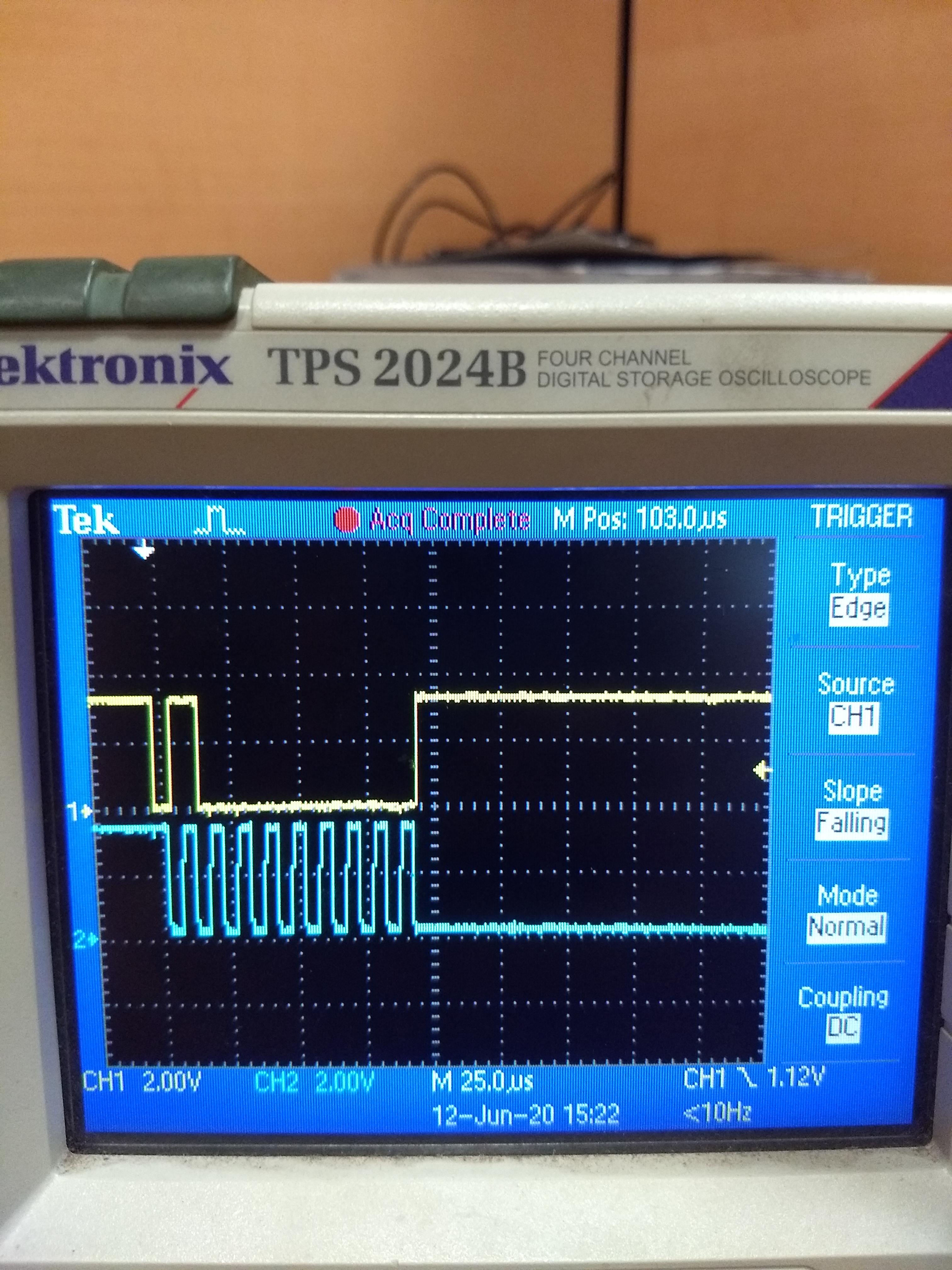
The above scope shot is obtained when I executed step (1) in the code. Slave address with write bit 0x80 and is acknowledged by the slave successfully.
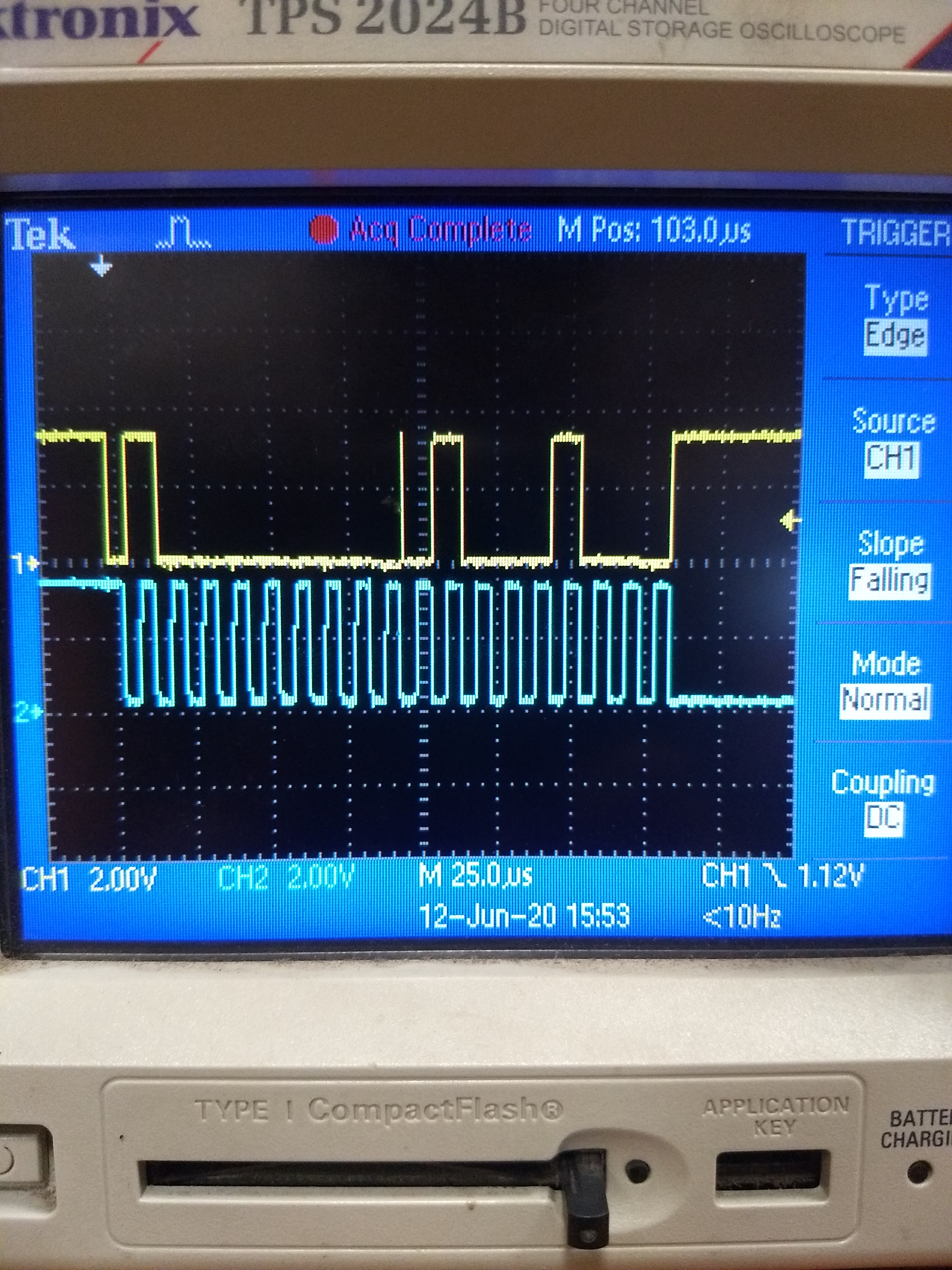
The above scope shot is obtained when I executed step (2) in the code. Slave address with write bit 0x80  for initiating a RESET  command to first slave. But at this point I am not receiving an acknowledgement but the same slave acknowledged to START signal in the previous step. After this step (2) I am not obtaining any response on the scope. Why this is happening?

And if  there is anything I can look into for a better understanding of I2C coding please let me know.


* I have checked for both slaves 0x40, 0x41 both  these salves acknowledge to START then there is no response from them.

* Also checked with an invalid address which returned NACK to START command itself.


Thank you,

Vineeth

  • You don't need to delay before setting the STP bit. You can set it immediately. The hardware won't actually send it until the data count counts down from I2CCNT to 0. Also, it looks like at some point in your code you change the number of bytes you're sending without updating I2CCNT.

    Can you try putting some while loops in your code to make sure you aren't moving on to the next transmission before the I2C flags say it's ready? This is a better approach than using delays and it will give us some more information about what is going wrong. For example, after you send the STP bit, wait until it is clear before moving on, or before you start a new transmission, check that the BB bit isn't set, etc...

    Please use the C2000Ware examples for reference and check out the tips on I2C here:

    http://processors.wiki.ti.com/index.php/I2C_Tips

    Whitney

  • Hi Whitney,

    Thank you for your quick response.

    I have edited my code as per your suggestions. The following is my code I am only concentrating for a successful write and read of configuration register 1.

            I2caRegs.I2CMDR.bit.IRS             = 0; // I2C is disabled
            I2caRegs.I2CPSC.bit.IPSC            = 9; // System clock divider value
            I2caRegs.I2CCLKL                    = 45; // Low time divider
            I2caRegs.I2CCLKH                    = 45; // High time divider
            I2caRegs.I2CMDR.bit.BC              = 0; // 8 bits per data byte
            I2caRegs.I2CMDR.bit.IRS             = 1; // I2C is enabled
    
            GpioDataRegs.GPBSET.bit.GPIO34      = 1; // ADC released from reset state
    
            I2caRegs.I2CSAR.bit.SAR             = 0x40; // Slave address register
            I2caRegs.I2CCNT                     = 1; // Data count
            I2caRegs.I2CMDR.bit.MST             = 1; // Master mode
            I2caRegs.I2CMDR.bit.TRX             = 1; // Transmitter mode
            I2caRegs.I2CMDR.bit.FREE            = 1; // I2C runs in free mode
            I2caRegs.I2CMDR.bit.STP             = 1; // Generate stop signal
            I2caRegs.I2CDXR.bit.DATA            = 0x06; // RESET command
            I2caRegs.I2CMDR.bit.STT             = 1; // Generate start signal (1)
    
            DELAY_US(20);
    
            while(I2caRegs.I2CSTR.bit.XRDY == 0 && I2caRegs.I2CMDR.bit.STP == 0)
            {
    
            }
    
            I2caRegs.I2CCNT                     = 2; // Data count
            I2caRegs.I2CMDR.bit.MST             = 1; // Master mode
            I2caRegs.I2CMDR.bit.TRX             = 1; // Transmitter mode
            I2caRegs.I2CMDR.bit.FREE            = 1; // I2C runs in free mode
            I2caRegs.I2CMDR.bit.STP             = 1; // Generate stop signal
            I2caRegs.I2CMDR.bit.STT             = 1; // Generate start signal (2)
            I2caRegs.I2CDXR.bit.DATA            = 0x44; // WREG command and Configuration register 1 address(3)
    
            while(I2caRegs.I2CSTR.bit.XRDY == 0)
                    {
    
                    }
    
            I2caRegs.I2CDXR.bit.DATA            = 0x02; // CR 1 data


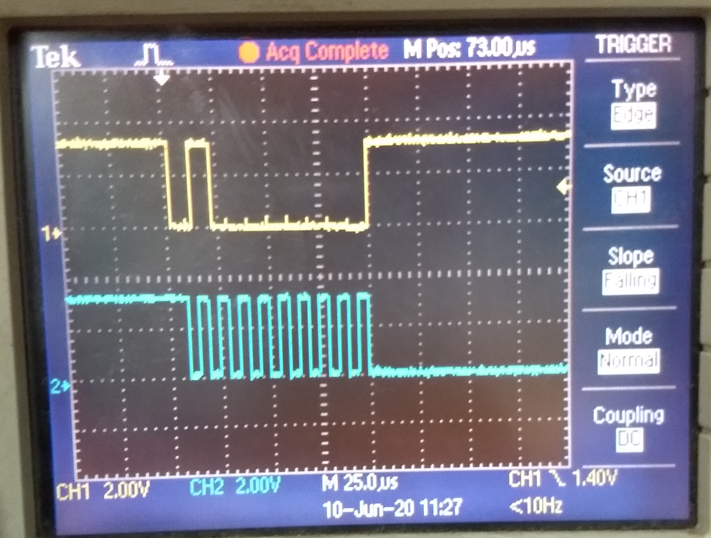
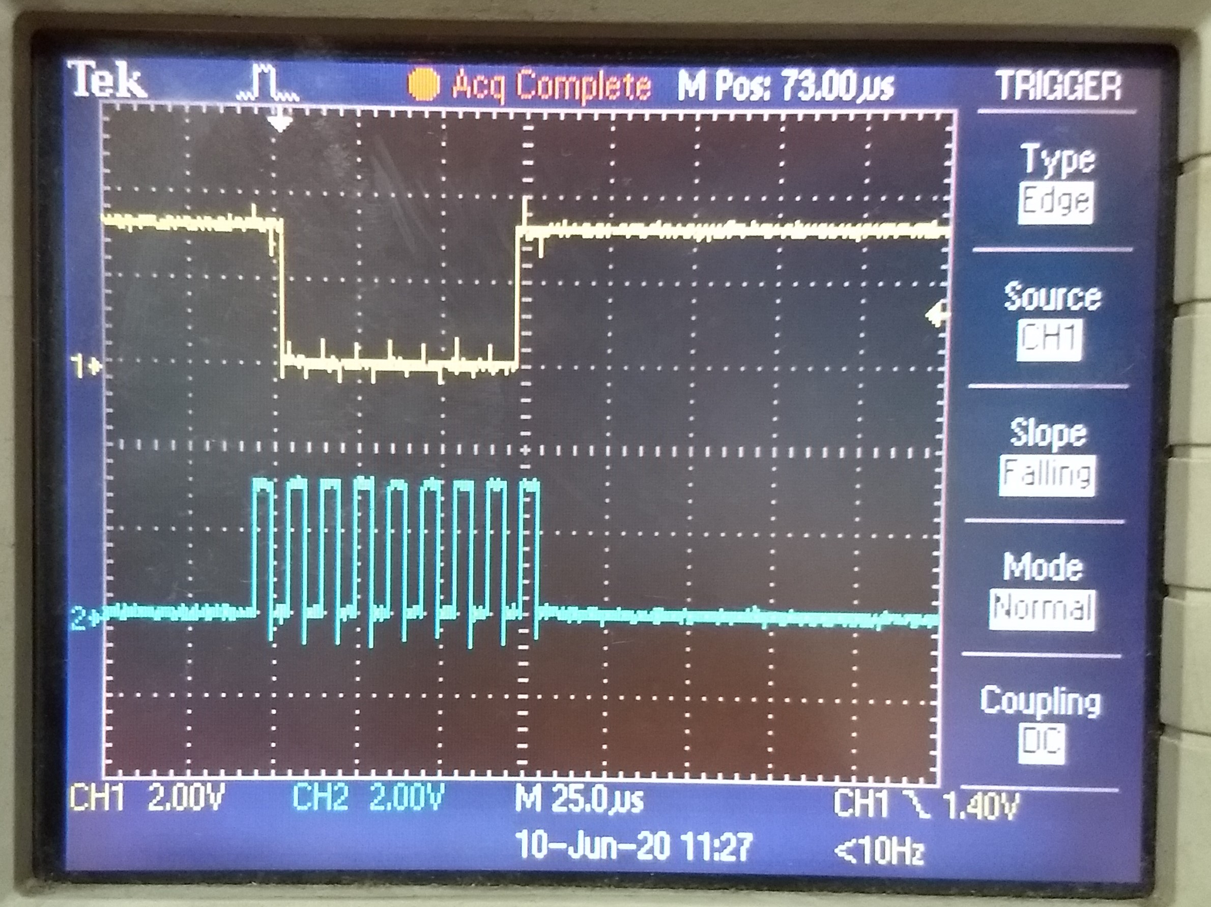
    Now I can acknowledge one byte transfer but not more. That is in first section of the code I have given data count 1 and wrote one data to I2CDXR then sent a START signal ( (1) in the code). The following is the scope result.

    And when I increase my data count to 2 and I am not using FIFO mode. I send START signal then first command 0x44 and second command 0x02 ( (2) and (3) in the code) after waiting for XRDY. The results I obtained are as follows.

    As we can see here the DATA 0X44 is clocked out successfully but it is not acknowledged by the slave why this happens?.

    After this I am receiving no response for command 0X02 and no STOP signal is generated. My data count is still 2.

    I observed another fashion in output when I moved the START condition just below command 0x44 that is 

    I2caRegs.I2CDXR.bit.DATA            = 0x44; // WREG command and Configuration register 1 address(3)
    I2caRegs.I2CMDR.bit.STT             = 1; // Generate start signal (2)
            

    I got these shots on scope 


    it is found that 0x44 is acknowledged. If write code like this 

            I2caRegs.I2CDXR.bit.DATA            = 0x44; // WREG command and Configuration register 1 address(3)
            I2caRegs.I2CDXR.bit.DATA            = 0x02; // CR 1 data
            I2caRegs.I2CMDR.bit.STT             = 1; // Generate start signal (2)

    only 0x02 is transferd and since the 0x44 is overwritten I think. 

    For configuration and reading back the same I need to send commands and START conditions back to back. How it is made possible. If you can give a simple bit field example it will be of great help. I have little knowledge in coding and I already gone through EEPROM example ( which I understood only a little ) and datasheet structures for commands.

    Is there is any importance in position of START condition? I have seen some examples where START and STOP is already set while configuring I2CMDR.

    Which all registers should be addressed while keeping i2c in reset mode (IRS = 0),  Since TRM specifies only IPSC register?

    Thank You,

    Vineeth

  • When you poll on I2CMDR.STP, you actually want to wait while it's equal to 1 as that means that the stop condition hasn't actually been sent yet. The hardware cleans STP after the stop has been sent or in the case of a NACK.

    Is there any particular reason why you aren't using the FIFO? You may want to consider enabling it so you can send those data bytes back-to-back without one overwriting the other.

    I don't think it matters much whether you send the STT before or after writing to the DXR register. Either way it won't send the data until the STT bit is set.

    Whitney

  • Hi Whitney,

    Thank you for your reply.

    Thank you for your suggestion on STP bit.

    The reason why I am not using FIFO is I have only little understanding about it and I haven`t seen  anything like i2c should be done only using FIFO.  And question still remains what should I do to write data back to back if am not using FIFO?. Like there should be some way out right?

    If it is in FIFO mode how can we check for STP or ARDY bit between each byte transfer, as it is happening all at once?

    I think we can send a START signal only by setting STT bit and I don`t see any other option. If the order of START signal doesn`t matter then why I am receiving different outputs for the same code, while I only changed START signal position. Primarily this was my question, and I have attached scope shots for the same in the previous thread. 

    Thank you,

    Vineeth

  • If you don't use the FIFO, you can't use back-to-back writes to DXR. You'll need to wait for XRDY status bit to be set before writing the second byte (which I believe you mentioned above). Is it possible that your slave device has some timing requirements where it can't toleration the gaps the address and data that you get when you set the STT bit first?

    Whitney

  • Hi Whitney,

    The main problem I have seen here is that when ever I set STT bit for a START condition the master appears to release START condition along with slave address and read/ write bit all at once. So even if for my data count 2 in section (2) of the code, if I issue START first followed by the data in next step the result is only START is acknowledged and not the following data. If I am giving START after first data that is 0x44 then both START and data is acknowledged by the slave. after this I am waiting for XRDY status and when it is ok, then I send next data 0x02. Transfer of this second data in this case is not giving any response I say.

    Thank you,

    Vineeth

  • As I said in the other thread, that's the expected behavior of the STT bit. If the slave device can't seem to handle the address and w/r bit being sent with a delay before the data, then do continue to wait until you have the data queued up in the FIFO before setting STT.

    I'd like to close this thread and just continue our conversation in the newer post, so we're not duplicating work. For the reference of anyone reading the thread, the new on is here:

    Whitney