This thread has been locked.

If you have a related question, please click the "Ask a related question" button in the top right corner. The newly created question will be automatically linked to this question.

TMS320F280049C: Feedback current reading for an Open loop VMC designed in Simulink differs from TI Application value

Part Number: TMS320F280049C
Other Parts Discussed in Thread: C2000WARE

Hi,

I've been trying to validate the Open loop VMC using the TI Application example as available for F280049c part of C2000Ware_DigitalPower_SDK_3_00_00_00 - tidm_dc_dc_buck.

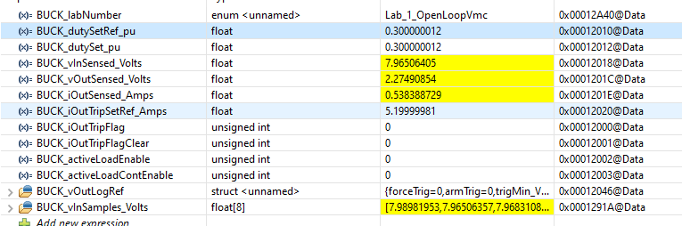
If i follow the C2000™ Digital Power Buck Converter BoosterPack™ Design Guide and check for the feedback current for 30% Duty Cycle I see 0.5A. As shown below:

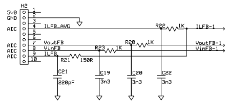
Which is in-line with

But when I model the same from Simulink ensuring PWM and ADC settings match 1:1 with TI application, I see a different reading.

What is strange is, the VOUT and VIN values are match between TI and Simulink. It is only the current reading.

As noted, I have ensured all the settings are in-line with TI application example.

There is one more point to consider:

Average load current = Vout/R = 2.27v/7.5ohm = 0.30A

Is there anything I'm missing here?

  • Hi,

    The Picture don't show up.

    Here is the one for Simulink generated code:

    Here is TI application running under same conditions:

    it is only the current value that differs.

  • Venkatesh,

    Can you confirm that you are monitoring the ILFB_AVG - H2[4] result and not ILFB - H2[9]?

    If you are monitoring ILFB_AVG as expected, I would recommend double-checking the conversion triggering and sequencing.  Even though the ILFB_AVG path has filtering, the cutoff frequency is too high to produce a DC feedback so the sampling point in time will make a difference in the current reading.

    The Vin and Vout signals have enough decoupling at the source to appear as DC.

    -Tommy

  • Hi Tommy,

    Thanks for the clue.

    I got it working.

    Missing part for this:

    //
    // BUCK_DRV_EPWM_UPDATE_LATENCY_TICKS - Estimated number of ePWM ticks
    // between the ADC trigger and ePWM TBPRD when duty cycle is shadow loaded.
    // Validate value by inspecting BUCK_isrDutyUpdateMinMargin_ticks.
    //
    #define BUCK_DRV_EPWM_UPDATE_LATENCY_TICKS ((uint16_t)185)
    #define BUCK_DRV_EPWM_ADC_TRIGGER_TBCTR (BUCK_DRV_EPWM_PERIOD_TICKS - BUCK_DRV_EPWM_UPDATE_LATENCY_TICKS)

    If you can explain me the idea behind this 185 counts would be very helpful.

  • Venkatesh,

    The ePWM is configured to generate the ADC trigger BUCK_DRV_EPWM_UPDATE_LATENCY_TICKS cycles before the end of the PWM cycle.

    The goal was to set BUCK_DRV_EPWM_UPDATE_LATENCY_TICKS to as small a value as possible so that the feedback sense and duty cycle update take place near the end of the PWM cycle.  The assumption being that this would mitigate switching noise, and it would minimize the time delay from duty cycle calculation to effective update.

    The BUCK_isrDutyUpdateMinMargin_ticks variable provides an estimate of the time between writing the new duty cycle value to the shadow register versus when the ePWM latches the shadow value for the next PWM cycle.  The value of BUCK_DRV_EPWM_UPDATE_LATENCY_TICKS can be adjusted experimentally based on the number of BUCK_isrDutyUpdateMinMargin_ticks cycles of slack measured.

    -Tommy

  • Hi Tommy,

    Thank you!

    So here is how I understand this:

    In order to mitigate the switching noise we do feedback sense near the end of PWM cycle, but care has to be taken such that we have enough time for duty calculations before ePWM latches the shadow value for next PWM cycle. So it is balance between mitigating effectively the switching noise as well as not missing out on duty update.

  • Yes, your understanding is correct.

    -Tommy