This thread has been locked.

If you have a related question, please click the "Ask a related question" button in the top right corner. The newly created question will be automatically linked to this question.

TMS320F28069: TMS320F28069PZT;I want to ask some question about TMS320F28069PZT;

Part Number: TMS320F28069


Hi  TI  Friends;

         I want to ask  some question  about TMS320F28069PZT;

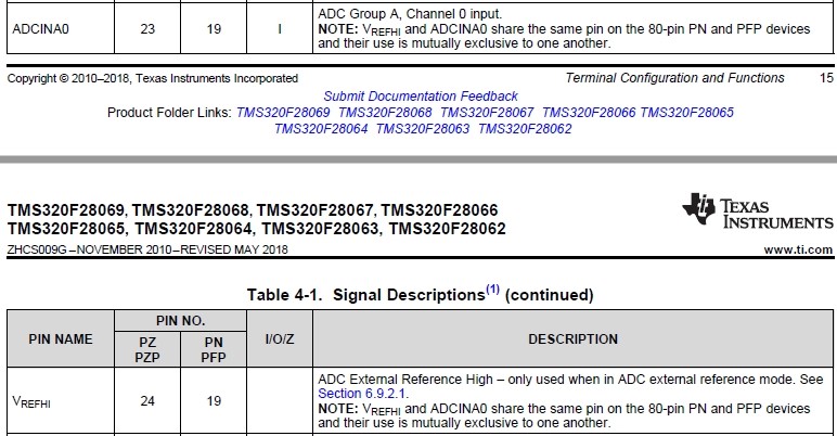
See below, peripheral definitions of TMS320F28069 are different from other DSP. VREFHI and ADCINA0 reuse one foot, which has the following questions.

1)      Datasheet show that VREFHI and ADCINA0 of 80-PIN TMS320F28069 PN and PFP Reuse one foot. Is 100-pin TMS320F28069PZT also multiplexed?

But the actual test found that 100-PIN TMS320F28069PZT VREFHI and ADCINA0 connected to different analog circuit sampling will have problems.

2)      DSP internal VREFHI and ADCINA0 are short connected? If the peripheral VREFHI is connected to the external reference voltage of 3V,

shall ADCINA0 also be shorted to 3V together, or to GND by shorting 1K resistance? Is there any DSP internal principle schematic reference?

3)      VREFHI and ADCINA0 reuse one foot, Is there a process in the internal software that requires special attention?

  • Tony,

    One point of clarity before I answer your original questions; the F28069 has two modes to provide the high reference to the ADC.  In internal mode the reference is provided from an internal bandgap and the full scale range is set to 3.3V.  If you want to provide your own high reference(from 2.4V - VDDIO) then you would supply that reference to the VREFHI pin of the device.  There is also a bit in the ADC control registers that has to be set to choose internal or external VREFHI

    On the 100-pin device the signals VREFHI and ADCINA0 do not share the same pin, so the functions can be used independently. That is I can use pin 23 to supply a conversion voltage to the ADCINA0 channel and if I desire to use an external reference I can put it on pin 24.

    On the 80-pin device since these are tied to the same pin the system can only use one of the functions.  If you want to use ADCINA0 you MUST select the internal reference for the ADC.  If you want to supply an external VREFHI, then you would place it on pin 19 and enabled it in SW, in this case there is no way to supply another voltage for channel ADCINA0.  You are free to convert this channel, but the ADC would be saturated at 4095 since you are effectively sampling the VREFHI signal, which also sets the full scale range upper limit.

    Best,

    Matthew