This thread has been locked.

If you have a related question, please click the "Ask a related question" button in the top right corner. The newly created question will be automatically linked to this question.

TMS320F28377D: EMIF daughter card

Part Number: TMS320F28377D
Other Parts Discussed in Thread: C2000WARE, TMDSCNCD28379D, LAUNCHXL-F28379D

Hello,

I'm looking for a reference design for TMS320F28377D interface to external memory (SDRAM/ NOR FLASH).

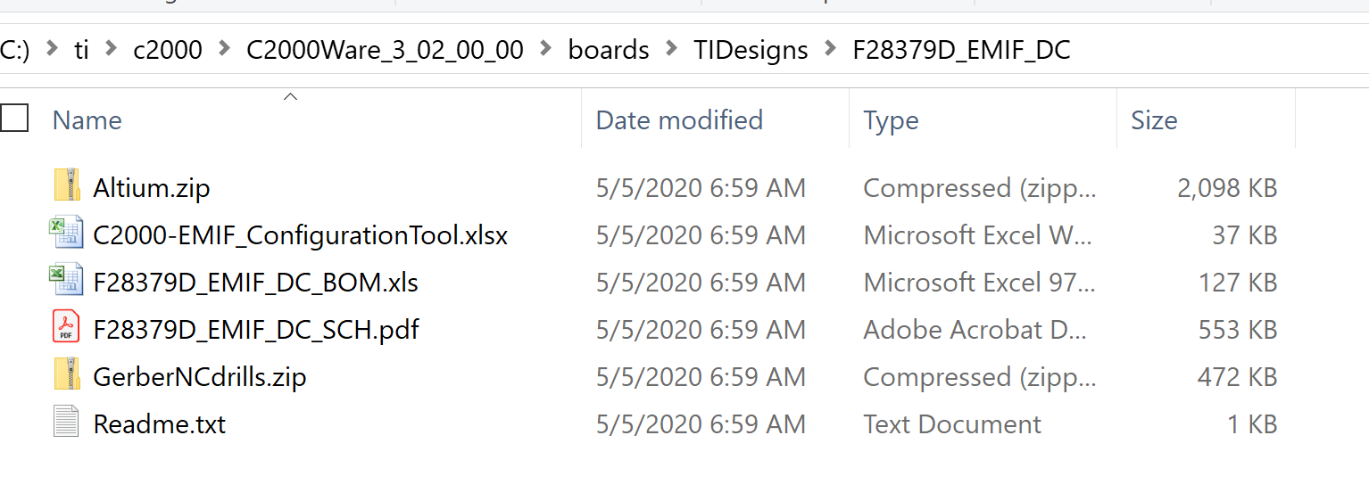
This app note https://www.ti.com/lit/an/sprac96a/sprac96a.pdf and several threads here refer to EMIF_DC being available as part of C2000Ware, but I see no such board on that page, neither there is an explicit fullclink to the relevant files.

Can you please assist?

Thanks,

David.

  • Hi David,

    I see all "EMIF_DC* files available in C2000Ware. Please see snapshot below (I see examples also).


    If you are not seeing it, please check if you have latest C2000Ware and make sure you are looking into right folder.

    Regards,

    Vivek Singh

  • Hi Vivek,

    Thanks , got it.

    Some additional questions:

    1. I'm interested in the SDRAM interface. The F28379D_EMIF_DC utilizes 256Mbit device. Can you suggest a pin compatible 512Mb device?
    2. Was the F28379D_EMIF_DC produced and tested with TMDSCNCD28379D ? I'm asking since the SDRAM are quite high speed signals, yet all three devices (SDRAM,SRAM,FLASH) share same nets, which creates significant stubs on the signals.

    Thanks,

    David.

  • David Dobrin said:
    I'm interested in the SDRAM interface. The F28379D_EMIF_DC utilizes 256Mbit device. Can you suggest a pin compatible 512Mb device?

    We are generally not supposed to recommend third party components. A distributor or SDRAM manufacturer might be able to help.

    David Dobrin said:
    Was the F28379D_EMIF_DC produced and tested with TMDSCNCD28379D ? I'm asking since the SDRAM are quite high speed signals, yet all three devices (SDRAM,SRAM,FLASH) share same nets, which creates significant stubs on the signals.

    Yes, the board was assembled and tested with both TMDSCNCD28379D and LAUNCHXL-F28379D. The IO buffers on F2837x were sized to drive multiple loads, and the board was designed with signal integrity in mind.

  • Hi,

    Understood.

    Looking more closely at  TMDSCNCD28379D and F28379D_EMIF_DC it seems that A12 is routed to jumper-mux that either connects it to GND either to GPIO. In addition EMIF design guidelines doc states (Table 10.) that it should be pulled low either by GPIO either to GND. So in either case it's pulled low.

    Does this mean that these boards do not provide access to full 256Mb of the SDRAM mounted on  F28379D_EMIF_DC?

    Where an example of connectivity that does provide full access can be found?

    Regards,

    David.

  • David,

    Your understanding is correct. The header is routed to EMIF2 on TMDSCNCD28379D, which has a smaller SDRAM address range than EMIF1 on LAUNCHXL-F28379D:

    -Tommy

  • Hi Tommy,

    Thanks for clarification.

    Now, looking at LAUNCHXL-F28379D r2.0:

    1. The D12 pin appears to be muxed with Boot Mode. Can you confirm this signal (D12) is indeed used in the SDRAM interface and the presence of the  switch doesn't interfere the correct operation?
    2. From the other side: doesn't the SDRAM interfere correct reading of the boot mode strap during power up? Were any provisions made to assure SDRAM's D12 is in high-Z during power up (eg. power sequence,... PU on DQM?...)?
    3. In case of running into troubles with the D12 pin conflict.... Documentation states that boot modes pins can be reconfigured (via programming OTP). Please advise what HW infrastructure is required to allow such programming? Which provision should I include in my board to make it possible?
    4. GPIO85_SCIRXDA, which is a default SCI boot interface, conflicts with EM1D0. As I understand the default SCI pins for boot can be reconfigured too. What HW provisions are required to do that?

    Regards,

    David.

  • David Dobrin said:
    The D12 pin appears to be muxed with Boot Mode. Can you confirm this signal (D12) is indeed used in the SDRAM interface and the presence of the  switch doesn't interfere the correct operation?

    Correct, D12 is a boot strap selection pin. A weak pull resistor is not expected to significantly impact the EMIF operation.

    David Dobrin said:
    From the other side: doesn't the SDRAM interfere correct reading of the boot mode strap during power up? Were any provisions made to assure SDRAM's D12 is in high-Z during power up (eg. power sequence,... PU on DQM?...)?

    The F2837x GPIO pins will boot as input pins, and the external memory will not output data unless a read operation is initiated. If everything goes as planned, neither device will be driving an active signal during boot. A weak pull-up can be placed on CS to ensure that the external memory is disabled until the EMIF is accessed.

    David Dobrin said:
    In case of running into troubles with the D12 pin conflict.... Documentation states that boot modes pins can be reconfigured (via programming OTP). Please advise what HW infrastructure is required to allow such programming? Which provision should I include in my board to make it possible?

    Correct, the remapping of boot strap pins is handled with OTP + Boot ROM software. The boot strap logic levels are read by the Boot ROM software (through GPIO) so the only hardware requirements are the pull resistors on the substitute pins.

    David Dobrin said:
    GPIO85_SCIRXDA, which is a default SCI boot interface, conflicts with EM1D0. As I understand the default SCI pins for boot can be reconfigured too. What HW provisions are required to do that?

    This is handled similarly to the substitute boot strap scheme. The Boot ROM will act according to the OTP key values.