Other Parts Discussed in Thread: DRV8353, , DRV8353RS-EVM
Hi,
I have a weird problem. I did my own hardware, based on an evaluation board. I'm using F28069F and DRV8353S.
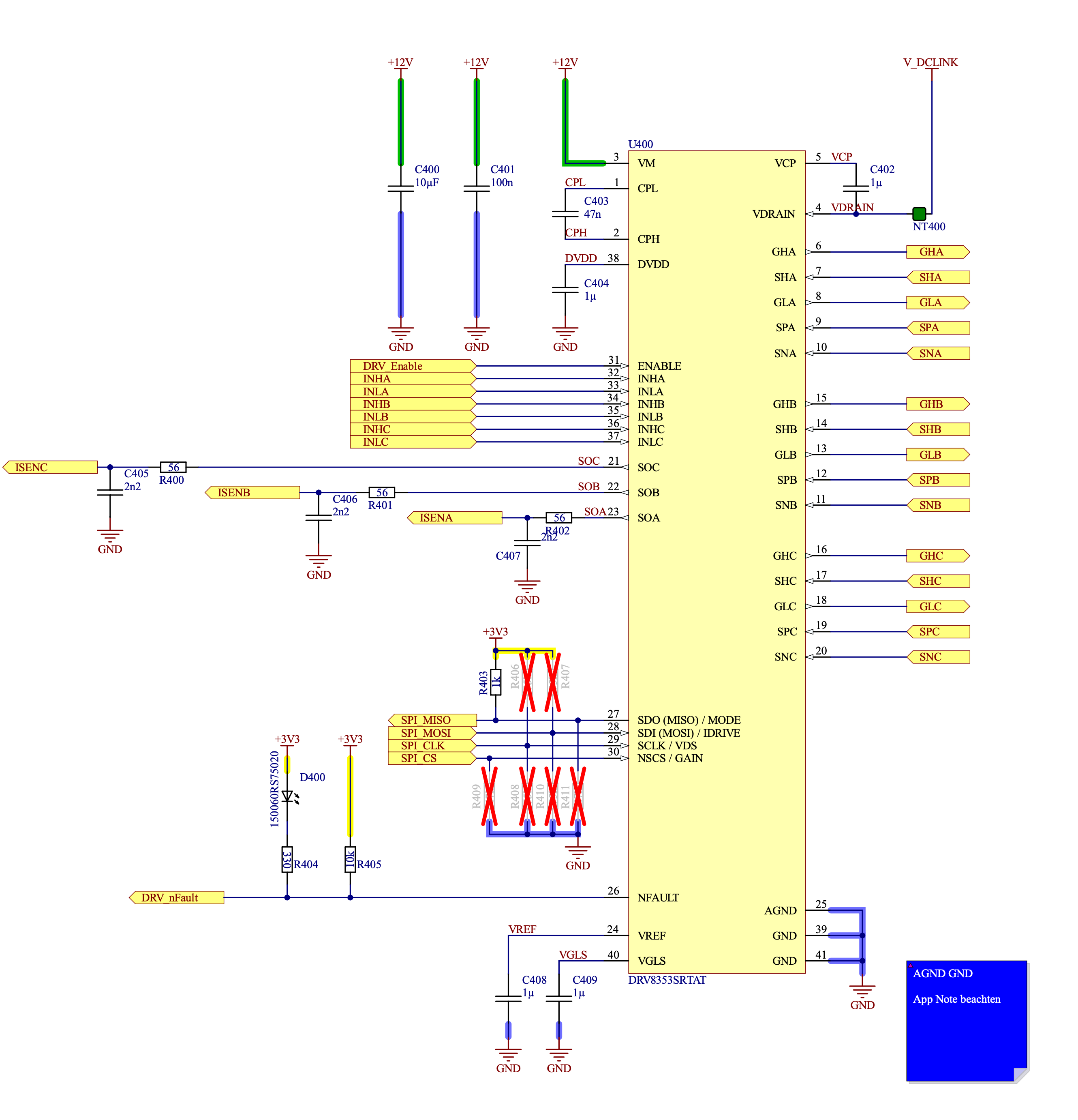
It is based on the DRV8353-EVM board.
But I can't get it working with lab02a, every time it tries to identify the motor, it fails.
What is happening?
RoverL - motor not spinning, but a noisy tone. Then it switches to EST_State_RS, motor start spinning for half a second or so and then a loud 'KLONK', debugging session aborts, voltage drops on supply power shortly...
I really do not know what I'm missing here...
I did change in the user.h the following:
USER_ADC_FULL_SCALE_VOLTAGE_V according to my Voltage divider (see attached schematic): (129.69) (slightly different to the EVM board, because I'm using 10k resistor instead of 9.76.
USER_ADC_FULL_SCALE_CURRENT_A (according to my Gain setting 10V/V) : 47.14 A (like DRV8353 EVM)
USER_VOLTAGE_FILTER_POLE_Hz according to my HW --> 347.49
Although I was so desperate, that I tried the modified project 05b from the evaluation board (which TI is providing) and motor does spin, but only when I disable Motor identification and I had to double the USER_ADC_FULL_SCALE_CURRENT_A to 94.28A value, but it is not correct then, but this would be not correct for my hardware. I disabled the PWMDataWrite and put 1A over the shunt resistor and I was able to see, that then the corresponding value in A was 2A instead of 1A. When I put it back to the correct value of 47.14A, then I see 1A when I apply 1A, motor does spin, but horribly. Motor makes a lot of noise. And as I said Motor Identification does not work regardless which current setting value.
this is my calculation for getting it back from the pu values:
gMotorVars.I_1_A = _IQmpy(gAdcData.I.value[0], _IQ(USER_IQ_FULL_SCALE_CURRENT_A));

  gMotorVars.I_2_A = _IQmpy(gAdcData.I.value[1], _IQ(USER_IQ_FULL_SCALE_CURRENT_A));

  gMotorVars.I_3_A = _IQmpy(gAdcData.I.value[2], _IQ(USER_IQ_FULL_SCALE_CURRENT_A));

  gMotorVars.V_1_A = _IQmpy(gAdcData.V.value[0], _IQ(USER_IQ_FULL_SCALE_VOLTAGE_V));

  gMotorVars.V_2_A = _IQmpy(gAdcData.V.value[1], _IQ(USER_IQ_FULL_SCALE_VOLTAGE_V));

  gMotorVars.V_3_A = _IQmpy(gAdcData.V.value[2], _IQ(USER_IQ_FULL_SCALE_VOLTAGE_V));
I checked and these values are really correct. So the measurement is ok from my point of view... What kind of other information does instaspin need ?
So, I do something miss here in the lab02b, but I do not know what...
Attached is my user.h, my project file, my hal.c,, hal.h, my drv8353.c and drv8353.h
/* --COPYRIGHT--,BSD
 * Copyright (c) 2012, Texas Instruments Incorporated
 * All rights reserved.
 *
 * Redistribution and use in source and binary forms, with or without
 * modification, are permitted provided that the following conditions
 * are met:
 *
 * *  Redistributions of source code must retain the above copyright
 *    notice, this list of conditions and the following disclaimer.
 *
 * *  Redistributions in binary form must reproduce the above copyright
 *    notice, this list of conditions and the following disclaimer in the
 *    documentation and/or other materials provided with the distribution.
 *
 * *  Neither the name of Texas Instruments Incorporated nor the names of
 *    its contributors may be used to endorse or promote products derived
 *    from this software without specific prior written permission.
 *
 * THIS SOFTWARE IS PROVIDED BY THE COPYRIGHT HOLDERS AND CONTRIBUTORS "AS IS"
 * AND ANY EXPRESS OR IMPLIED WARRANTIES, INCLUDING, BUT NOT LIMITED TO,
 * THE IMPLIED WARRANTIES OF MERCHANTABILITY AND FITNESS FOR A PARTICULAR
 * PURPOSE ARE DISCLAIMED. IN NO EVENT SHALL THE COPYRIGHT OWNER OR
 * CONTRIBUTORS BE LIABLE FOR ANY DIRECT, INDIRECT, INCIDENTAL, SPECIAL,
 * EXEMPLARY, OR CONSEQUENTIAL DAMAGES (INCLUDING, BUT NOT LIMITED TO,
 * PROCUREMENT OF SUBSTITUTE GOODS OR SERVICES; LOSS OF USE, DATA, OR PROFITS;
 * OR BUSINESS INTERRUPTION) HOWEVER CAUSED AND ON ANY THEORY OF LIABILITY,
 * WHETHER IN CONTRACT, STRICT LIABILITY, OR TORT (INCLUDING NEGLIGENCE OR
 * OTHERWISE) ARISING IN ANY WAY OUT OF THE USE OF THIS SOFTWARE,
 * EVEN IF ADVISED OF THE POSSIBILITY OF SUCH DAMAGE.
 * --/COPYRIGHT--*/
//! \file   solutions/instaspin_foc/src/proj_lab02a.c
//! \brief Using InstaSPIN�FOC for the first time, Motor ID, full control system from ROM
//!
//! (C) Copyright 2011, Texas Instruments, Inc.

//! \defgroup PROJ_LAB02a PROJ_LAB02a
//@{

//! \defgroup PROJ_LAB02a_OVERVIEW Project Overview
//!
//! Using InstaSPIN�FOC for the first time, Motor ID, full control system from ROM
//!

// **************************************************************************
// the includes

// system includes
#include <math.h>
#include "main.h"

#ifdef FLASH
#pragma CODE_SECTION(mainISR,"ramfuncs");
#endif

// Include header files used in the main function


// **************************************************************************
// the defines

#define LED_BLINK_FREQ_Hz   5


// **************************************************************************
// the globals

uint_least16_t gCounter_updateGlobals = 0;

bool Flag_Latch_softwareUpdate = true;

CTRL_Handle ctrlHandle;

#ifdef CSM_ENABLE
#pragma DATA_SECTION(halHandle,"rom_accessed_data");
#endif

HAL_Handle halHandle;

#ifdef CSM_ENABLE
#pragma DATA_SECTION(gUserParams,"rom_accessed_data");
#endif

USER_Params gUserParams;

HAL_PwmData_t gPwmData = {_IQ(0.0), _IQ(0.0), _IQ(0.0)};

HAL_AdcData_t gAdcData;

_iq gMaxCurrentSlope = _IQ(0.0);

#ifdef FAST_ROM_V1p6
CTRL_Obj *controller_obj;
#else

#ifdef CSM_ENABLE
#pragma DATA_SECTION(ctrl,"rom_accessed_data");
#endif

CTRL_Obj ctrl;				//v1p7 format
#endif

uint16_t gLEDcnt = 0;

volatile MOTOR_Vars_t gMotorVars = MOTOR_Vars_INIT;

#ifdef FLASH
// Used for running BackGround in flash, and ISR in RAM
extern uint16_t *RamfuncsLoadStart, *RamfuncsLoadEnd, *RamfuncsRunStart;

#ifdef CSM_ENABLE
extern uint16_t *econst_start, *econst_end, *econst_ram_load;
extern uint16_t *switch_start, *switch_end, *switch_ram_load;
#endif
#endif

#ifdef DRV8301_SPI
// Watch window interface to the 8301 SPI
DRV_SPI_8301_Vars_t gDrvSpi8301Vars;
#endif

#ifdef DRV8305_SPI
// Watch window interface to the 8305 SPI
DRV_SPI_8305_Vars_t gDrvSpi8305Vars;
#endif
#ifdef DRV8353_SPI
// Watch window interface to the 8305 SPI
DRV_SPI_8353_Vars_t gDrvSpi8353Vars;
#endif
// **************************************************************************
// the functions

void main(void)
{
  uint_least8_t estNumber = 0;

#ifdef FAST_ROM_V1p6
  uint_least8_t ctrlNumber = 0;
#endif

  // Only used if running from FLASH
  // Note that the variable FLASH is defined by the project
  #ifdef FLASH
  // Copy time critical code and Flash setup code to RAM
  // The RamfuncsLoadStart, RamfuncsLoadEnd, and RamfuncsRunStart
  // symbols are created by the linker. Refer to the linker files.
  memCopy((uint16_t *)&RamfuncsLoadStart,(uint16_t *)&RamfuncsLoadEnd,(uint16_t *)&RamfuncsRunStart);

  #ifdef CSM_ENABLE
  //copy .econst to unsecure RAM
  if(*econst_end - *econst_start)
  {
     memCopy((uint16_t *)&econst_start,(uint16_t *)&econst_end,(uint16_t *)&econst_ram_load);
  }

  //copy .switch ot unsecure RAM
  if(*switch_end - *switch_start)
  {
    memCopy((uint16_t *)&switch_start,(uint16_t *)&switch_end,(uint16_t *)&switch_ram_load);
  }
  #endif
  #endif

  // initialize the hardware abstraction layer
  halHandle = HAL_init(&hal,sizeof(hal));


  // check for errors in user parameters
  USER_checkForErrors(&gUserParams);


  // store user parameter error in global variable
  gMotorVars.UserErrorCode = USER_getErrorCode(&gUserParams);


  // do not allow code execution if there is a user parameter error
  if(gMotorVars.UserErrorCode != USER_ErrorCode_NoError)
    {
      for(;;)
        {
          gMotorVars.Flag_enableSys = false;
        }
    }


  // initialize the user parameters
  USER_setParams(&gUserParams);


  // set the hardware abstraction layer parameters
  HAL_setParams(halHandle,&gUserParams);


  // initialize the controller
#ifdef FAST_ROM_V1p6
  ctrlHandle = CTRL_initCtrl(ctrlNumber, estNumber);  		//v1p6 format (06xF and 06xM devices)
  controller_obj = (CTRL_Obj *)ctrlHandle;
#else
  ctrlHandle = CTRL_initCtrl(estNumber,&ctrl,sizeof(ctrl));	//v1p7 format default
#endif


  {
    CTRL_Version version;

    // get the version number
    CTRL_getVersion(ctrlHandle,&version);

    gMotorVars.CtrlVersion = version;
  }


  // set the default controller parameters
  CTRL_setParams(ctrlHandle,&gUserParams);


  // setup faults
  HAL_setupFaults(halHandle);


  // initialize the interrupt vector table
  HAL_initIntVectorTable(halHandle);


  // enable the ADC interrupts
  HAL_enableAdcInts(halHandle);


  // enable global interrupts
  HAL_enableGlobalInts(halHandle);


  // enable debug interrupts
  HAL_enableDebugInt(halHandle);


  // disable the PWM
  HAL_disablePwm(halHandle);


#ifdef DRV8301_SPI
  // turn on the DRV8301 if present
  HAL_enableDrv(halHandle);
  // initialize the DRV8301 interface
  HAL_setupDrvSpi(halHandle,&gDrvSpi8301Vars);
#endif

#ifdef DRV8305_SPI
  // turn on the DRV8305 if present
  HAL_enableDrv(halHandle);
  // initialize the DRV8305 interface
  HAL_setupDrvSpi(halHandle,&gDrvSpi8305Vars);
#endif
#ifdef DRV8353
  HAL_enableDrv(halHandle);
#endif
#ifdef DRV8353_SPI
  // initialize the DRV8353 interface
      HAL_setupDrvSpi(halHandle,&gDrvSpi8353Vars);
#endif
  // enable DC bus compensation
  CTRL_setFlag_enableDcBusComp(ctrlHandle, true);


  for(;;)
  {
    // Waiting for enable system flag to be set
    while(!(gMotorVars.Flag_enableSys));

    // loop while the enable system flag is true
    while(gMotorVars.Flag_enableSys)
      {
        CTRL_Obj *obj = (CTRL_Obj *)ctrlHandle;

        // increment counters
        gCounter_updateGlobals++;


        if(CTRL_isError(ctrlHandle))
          {
            // set the enable controller flag to false
            CTRL_setFlag_enableCtrl(ctrlHandle,false);

            // set the enable system flag to false
            gMotorVars.Flag_enableSys = false;

            // disable the PWM
            HAL_disablePwm(halHandle);
          }
        else
          {
            // update the controller state
            bool flag_ctrlStateChanged = CTRL_updateState(ctrlHandle);

            // enable or disable the control
            CTRL_setFlag_enableCtrl(ctrlHandle, gMotorVars.Flag_Run_Identify);

            if(flag_ctrlStateChanged)
              {
                CTRL_State_e ctrlState = CTRL_getState(ctrlHandle);
                EST_State_e estState = EST_getState(obj->estHandle);

                if(ctrlState == CTRL_State_OffLine)
                  {
                    // enable the PWM
                    HAL_enablePwm(halHandle);
                  }
                else if(ctrlState == CTRL_State_OnLine)
                  {
                    if((estState < EST_State_LockRotor) || (estState > EST_State_MotorIdentified))
                      {
                        // update the ADC bias values
                        HAL_updateAdcBias(halHandle);
                      }

                    // Return the bias value for currents
                    gMotorVars.I_bias.value[0] = HAL_getBias(halHandle,HAL_SensorType_Current,0);
                    gMotorVars.I_bias.value[1] = HAL_getBias(halHandle,HAL_SensorType_Current,1);
                    gMotorVars.I_bias.value[2] = HAL_getBias(halHandle,HAL_SensorType_Current,2);

                    // Return the bias value for voltages
                    gMotorVars.V_bias.value[0] = HAL_getBias(halHandle,HAL_SensorType_Voltage,0);
                    gMotorVars.V_bias.value[1] = HAL_getBias(halHandle,HAL_SensorType_Voltage,1);
                    gMotorVars.V_bias.value[2] = HAL_getBias(halHandle,HAL_SensorType_Voltage,2);

                    // enable the PWM
                    HAL_enablePwm(halHandle);
                  }
                else if(ctrlState == CTRL_State_Idle)
                  {
                    // disable the PWM
                    HAL_disablePwm(halHandle);
                    gMotorVars.Flag_Run_Identify = false;
                  }

                if((CTRL_getFlag_enableUserMotorParams(ctrlHandle) == true) &&
                  (ctrlState > CTRL_State_Idle) &&
                  (gMotorVars.CtrlVersion.minor == 6))
                  {
                    // call this function to fix 1p6
                    USER_softwareUpdate1p6(ctrlHandle);
                  }

              }
          }


        if(EST_isMotorIdentified(obj->estHandle))
          {
            // set the current ramp
            EST_setMaxCurrentSlope_pu(obj->estHandle,gMaxCurrentSlope);
            gMotorVars.Flag_MotorIdentified = true;

            // set the speed reference
            CTRL_setSpd_ref_krpm(ctrlHandle,gMotorVars.SpeedRef_krpm);

            // set the speed acceleration
            CTRL_setMaxAccel_pu(ctrlHandle,_IQmpy(MAX_ACCEL_KRPMPS_SF,gMotorVars.MaxAccel_krpmps));

            if(Flag_Latch_softwareUpdate)
            {
              Flag_Latch_softwareUpdate = false;

              USER_calcPIgains(ctrlHandle);
            }

          }
        else
          {
            Flag_Latch_softwareUpdate = true;

            // the estimator sets the maximum current slope during identification
            gMaxCurrentSlope = EST_getMaxCurrentSlope_pu(obj->estHandle);
          }


        // when appropriate, update the global variables
        if(gCounter_updateGlobals >= NUM_MAIN_TICKS_FOR_GLOBAL_VARIABLE_UPDATE)
          {
            // reset the counter
            gCounter_updateGlobals = 0;

            updateGlobalVariables_motor(ctrlHandle);
          }

        // recalculate Kp and Ki gains to fix the R/L limitation of 2000.0, and Kp limit to 0.11
        recalcKpKi(ctrlHandle);

        if(CTRL_getMotorType(ctrlHandle) == MOTOR_Type_Induction)
          {
            // set electrical frequency limit to zero while identifying an induction motor
            setFeLimitZero(ctrlHandle);

            // calculate Dir_qFmt for acim motors
            acim_Dir_qFmtCalc(ctrlHandle);
          }

        // enable/disable the forced angle
        EST_setFlag_enableForceAngle(obj->estHandle,gMotorVars.Flag_enableForceAngle);

        // enable or disable power warp
        CTRL_setFlag_enablePowerWarp(ctrlHandle,gMotorVars.Flag_enablePowerWarp);

#ifdef DRV8301_SPI
        HAL_writeDrvData(halHandle,&gDrvSpi8301Vars);

        HAL_readDrvData(halHandle,&gDrvSpi8301Vars);
#endif
#ifdef DRV8305_SPI
        HAL_writeDrvData(halHandle,&gDrvSpi8305Vars);

        HAL_readDrvData(halHandle,&gDrvSpi8305Vars);
#endif
#ifdef DRV8353_SPI
            HAL_writeDrvData(halHandle,&gDrvSpi8353Vars);

            HAL_readDrvData(halHandle,&gDrvSpi8353Vars);
#endif
      } // end of while(gFlag_enableSys) loop


    // disable the PWM
    HAL_disablePwm(halHandle);

    // set the default controller parameters (Reset the control to re-identify the motor)
    CTRL_setParams(ctrlHandle,&gUserParams);
    gMotorVars.Flag_Run_Identify = false;

  } // end of for(;;) loop

} // end of main() function


interrupt void mainISR(void)
{
  HAL_PwmData_t negPwmData = {_IQ(0.0), _IQ(0.0), _IQ(0.0)};


  // acknowledge the ADC interrupt
  HAL_acqAdcInt(halHandle,ADC_IntNumber_1);


  // convert the ADC data
  HAL_readAdcData(halHandle,&gAdcData);


  // run the controller
  CTRL_run(ctrlHandle,halHandle,&gAdcData,&negPwmData);


  // negate PwmData generated by SVGEN module in ROM
  gPwmData.Tabc.value[0] = _IQmpy(negPwmData.Tabc.value[0], _IQ(-1.0));
  gPwmData.Tabc.value[1] = _IQmpy(negPwmData.Tabc.value[1], _IQ(-1.0));
  gPwmData.Tabc.value[2] = _IQmpy(negPwmData.Tabc.value[2], _IQ(-1.0));


  // write the PWM compare values
  HAL_writePwmData(halHandle,&gPwmData);


  // setup the controller
  CTRL_setup(ctrlHandle);


  return;
} // end of mainISR() function


void updateGlobalVariables_motor(CTRL_Handle handle)
{
  CTRL_Obj *obj = (CTRL_Obj *)handle;

  // get the speed estimate
  gMotorVars.Speed_krpm = EST_getSpeed_krpm(obj->estHandle);

  // get the real time speed reference coming out of the speed trajectory generator
  gMotorVars.SpeedTraj_krpm = _IQmpy(CTRL_getSpd_int_ref_pu(handle),EST_get_pu_to_krpm_sf(obj->estHandle));

  // get the magnetizing current
  gMotorVars.MagnCurr_A = EST_getIdRated(obj->estHandle);

  // get the rotor resistance
  gMotorVars.Rr_Ohm = EST_getRr_Ohm(obj->estHandle);

  // get the stator resistance
  gMotorVars.Rs_Ohm = EST_getRs_Ohm(obj->estHandle);

  // get the stator inductance in the direct coordinate direction
  gMotorVars.Lsd_H = EST_getLs_d_H(obj->estHandle);

  // get the stator inductance in the quadrature coordinate direction
  gMotorVars.Lsq_H = EST_getLs_q_H(obj->estHandle);

  // get the flux
  gMotorVars.Flux_VpHz = EST_getFlux_VpHz(obj->estHandle);

  // get the controller state
  gMotorVars.CtrlState = CTRL_getState(handle);

  // get the estimator state
  gMotorVars.EstState = EST_getState(obj->estHandle);

  // Get the DC buss voltage
  gMotorVars.VdcBus_kV = _IQmpy(gAdcData.dcBus,_IQ(USER_IQ_FULL_SCALE_VOLTAGE_V/1000.0));

  return;
} // end of updateGlobalVariables_motor() function


void recalcKpKi(CTRL_Handle handle)
{
  CTRL_Obj *obj = (CTRL_Obj *)handle;
  EST_State_e EstState = EST_getState(obj->estHandle);

  if((EST_isMotorIdentified(obj->estHandle) == false) && (EstState == EST_State_Rs))
    {
      float_t Lhf = CTRL_getLhf(handle);
      float_t Rhf = CTRL_getRhf(handle);
      float_t RhfoverLhf = Rhf/Lhf;
      _iq Kp = _IQ(0.25*Lhf*USER_IQ_FULL_SCALE_CURRENT_A/(USER_CTRL_PERIOD_sec*USER_IQ_FULL_SCALE_VOLTAGE_V));
      _iq Ki = _IQ(RhfoverLhf*USER_CTRL_PERIOD_sec);

      // set Rhf/Lhf
      CTRL_setRoverL(handle,RhfoverLhf);

      // set the controller proportional gains
      CTRL_setKp(handle,CTRL_Type_PID_Id,Kp);
      CTRL_setKp(handle,CTRL_Type_PID_Iq,Kp);

      // set the Id controller gains
      CTRL_setKi(handle,CTRL_Type_PID_Id,Ki);
      PID_setKi(obj->pidHandle_Id,Ki);

      // set the Iq controller gains
      CTRL_setKi(handle,CTRL_Type_PID_Iq,Ki);
      PID_setKi(obj->pidHandle_Iq,Ki);
    }

  return;
} // end of recalcKpKi() function


void setFeLimitZero(CTRL_Handle handle)
{
  CTRL_Obj *obj = (CTRL_Obj *)handle;
  EST_State_e EstState = EST_getState(obj->estHandle);

  _iq fe_neg_max_pu;
  _iq fe_pos_min_pu;

  if((EST_isMotorIdentified(obj->estHandle) == false) && (CTRL_getMotorType(handle) == MOTOR_Type_Induction))
    {
	  fe_neg_max_pu = _IQ30(0.0);

	  fe_pos_min_pu = _IQ30(0.0);
    }
  else
    {
	  fe_neg_max_pu = _IQ30(-USER_ZEROSPEEDLIMIT);

	  fe_pos_min_pu = _IQ30(USER_ZEROSPEEDLIMIT);
    }

  EST_setFe_neg_max_pu(obj->estHandle, fe_neg_max_pu);

  EST_setFe_pos_min_pu(obj->estHandle, fe_pos_min_pu);

  return;
} // end of setFeLimitZero() function


void acim_Dir_qFmtCalc(CTRL_Handle handle)
{
  CTRL_Obj *obj = (CTRL_Obj *)handle;
  EST_State_e EstState = EST_getState(obj->estHandle);

  if(EstState == EST_State_IdRated)
    {
      EST_setDir_qFmt(obj->estHandle, EST_computeDirection_qFmt(obj->estHandle, 0.7));
    }

  return;
} // end of acim_Dir_qFmtCalc() function


//@} //defgroup
// end of file
/* --COPYRIGHT--,BSD
 * Copyright (c) 2012, Texas Instruments Incorporated
 * All rights reserved.
 *
 * Redistribution and use in source and binary forms, with or without
 * modification, are permitted provided that the following conditions
 * are met:
 *
 * *  Redistributions of source code must retain the above copyright
 *    notice, this list of conditions and the following disclaimer.
 *
 * *  Redistributions in binary form must reproduce the above copyright
 *    notice, this list of conditions and the following disclaimer in the
 *    documentation and/or other materials provided with the distribution.
 *
 * *  Neither the name of Texas Instruments Incorporated nor the names of
 *    its contributors may be used to endorse or promote products derived
 *    from this software without specific prior written permission.
 *
 * THIS SOFTWARE IS PROVIDED BY THE COPYRIGHT HOLDERS AND CONTRIBUTORS "AS IS"
 * AND ANY EXPRESS OR IMPLIED WARRANTIES, INCLUDING, BUT NOT LIMITED TO,
 * THE IMPLIED WARRANTIES OF MERCHANTABILITY AND FITNESS FOR A PARTICULAR
 * PURPOSE ARE DISCLAIMED. IN NO EVENT SHALL THE COPYRIGHT OWNER OR
 * CONTRIBUTORS BE LIABLE FOR ANY DIRECT, INDIRECT, INCIDENTAL, SPECIAL,
 * EXEMPLARY, OR CONSEQUENTIAL DAMAGES (INCLUDING, BUT NOT LIMITED TO,
 * PROCUREMENT OF SUBSTITUTE GOODS OR SERVICES; LOSS OF USE, DATA, OR PROFITS;
 * OR BUSINESS INTERRUPTION) HOWEVER CAUSED AND ON ANY THEORY OF LIABILITY,
 * WHETHER IN CONTRACT, STRICT LIABILITY, OR TORT (INCLUDING NEGLIGENCE OR
 * OTHERWISE) ARISING IN ANY WAY OUT OF THE USE OF THIS SOFTWARE,
 * EVEN IF ADVISED OF THE POSSIBILITY OF SUCH DAMAGE.
 * --/COPYRIGHT--*/
//! \file   solutions/instaspin_foc/boards/drv8301kit_revD/f28x/f2806xF/src/hal.c
//! \brief Contains the various functions related to the HAL object (everything outside the CTRL system)
//!
//! (C) Copyright 2011, Texas Instruments, Inc.


// **************************************************************************
// the includes

// drivers

// modules

// platforms
#include "hal.h"
#include "user.h"
#include "hal_obj.h"

#ifdef FLASH
#pragma CODE_SECTION(HAL_setupFlash,"ramfuncs");
#endif

// **************************************************************************
// the defines

#define US_TO_CNT(A) ((((long double) A * (long double)USER_SYSTEM_FREQ_MHz) - 9.0L) / 5.0L)

// **************************************************************************
// the globals

HAL_Obj hal;


// **************************************************************************
// the functions

void HAL_cal(HAL_Handle handle)
{
  HAL_Obj *obj = (HAL_Obj *)handle;


  // enable the ADC clock
  CLK_enableAdcClock(obj->clkHandle);


  // Run the Device_cal() function
  // This function copies the ADC and oscillator calibration values from TI reserved
  // OTP into the appropriate trim registers
  // This boot ROM automatically calls this function to calibrate the interal
  // oscillators and ADC with device specific calibration data.
  // If the boot ROM is bypassed by Code Composer Studio during the development process,
  // then the calibration must be initialized by the application
  ENABLE_PROTECTED_REGISTER_WRITE_MODE;
  (*Device_cal)();
  DISABLE_PROTECTED_REGISTER_WRITE_MODE;

  // run offsets calibration in user's memory
  HAL_AdcOffsetSelfCal(handle);

  // run oscillator compensation
  HAL_OscTempComp(handle);

  // disable the ADC clock
  CLK_disableAdcClock(obj->clkHandle);

  return;
} // end of HAL_cal() function


void HAL_OscTempComp(HAL_Handle handle)
{
  HAL_Obj *obj = (HAL_Obj *)handle;
  uint16_t Temperature;

  // disable the ADCs
  ADC_disable(obj->adcHandle);

  // power up the bandgap circuit
  ADC_enableBandGap(obj->adcHandle);

  // set the ADC voltage reference source to internal
  ADC_setVoltRefSrc(obj->adcHandle,ADC_VoltageRefSrc_Int);

  // enable the ADC reference buffers
  ADC_enableRefBuffers(obj->adcHandle);

  // Set main clock scaling factor (max45MHz clock for the ADC module)
  ADC_setDivideSelect(obj->adcHandle,ADC_DivideSelect_ClkIn_by_2);

  // power up the ADCs
  ADC_powerUp(obj->adcHandle);

  // enable the ADCs
  ADC_enable(obj->adcHandle);

  // enable non-overlap mode
  ADC_enableNoOverlapMode(obj->adcHandle);

  // connect channel A5 internally to the temperature sensor
  ADC_setTempSensorSrc(obj->adcHandle, ADC_TempSensorSrc_Int);

  // set SOC0 channel select to ADCINA5
  ADC_setSocChanNumber(obj->adcHandle, ADC_SocNumber_0, ADC_SocChanNumber_A5);

  // set SOC0 acquisition period to 26 ADCCLK
  ADC_setSocSampleDelay(obj->adcHandle, ADC_SocNumber_0, ADC_SocSampleDelay_64_cycles);

  // connect ADCINT1 to EOC0
  ADC_setIntSrc(obj->adcHandle, ADC_IntNumber_1, ADC_IntSrc_EOC0);

  // clear ADCINT1 flag
  ADC_clearIntFlag(obj->adcHandle, ADC_IntNumber_1);

  // enable ADCINT1
  ADC_enableInt(obj->adcHandle, ADC_IntNumber_1);

  // force start of conversion on SOC0
  ADC_setSocFrc(obj->adcHandle, ADC_SocFrc_0);

  // wait for end of conversion
  while (ADC_getIntFlag(obj->adcHandle, ADC_IntNumber_1) == 0){}

  // clear ADCINT1 flag
  ADC_clearIntFlag(obj->adcHandle, ADC_IntNumber_1);

  Temperature = ADC_readResult(obj->adcHandle, ADC_ResultNumber_0);

  HAL_osc1Comp(handle, Temperature);

  HAL_osc2Comp(handle, Temperature);

  return;
} // end of HAL_OscTempComp() function


void HAL_osc1Comp(HAL_Handle handle, const int16_t sensorSample)
{
	int16_t compOscFineTrim;
	HAL_Obj *obj = (HAL_Obj *)handle;

	ENABLE_PROTECTED_REGISTER_WRITE_MODE;

    compOscFineTrim = ((sensorSample - getRefTempOffset())*(int32_t)getOsc1FineTrimSlope()
                      + OSC_POSTRIM_OFF + FP_ROUND )/FP_SCALE + getOsc1FineTrimOffset() - OSC_POSTRIM;

    if(compOscFineTrim > 31)
      {
        compOscFineTrim = 31;
      }
	else if(compOscFineTrim < -31)
      {
        compOscFineTrim = -31;
      }

    OSC_setTrim(obj->oscHandle, OSC_Number_1, HAL_getOscTrimValue(getOsc1CoarseTrim(), compOscFineTrim));

    DISABLE_PROTECTED_REGISTER_WRITE_MODE;

    return;
} // end of HAL_osc1Comp() function


void HAL_osc2Comp(HAL_Handle handle, const int16_t sensorSample)
{
	int16_t compOscFineTrim;
	HAL_Obj *obj = (HAL_Obj *)handle;

	ENABLE_PROTECTED_REGISTER_WRITE_MODE;

    compOscFineTrim = ((sensorSample - getRefTempOffset())*(int32_t)getOsc2FineTrimSlope()
                      + OSC_POSTRIM_OFF + FP_ROUND )/FP_SCALE + getOsc2FineTrimOffset() - OSC_POSTRIM;

    if(compOscFineTrim > 31)
      {
        compOscFineTrim = 31;
      }
	else if(compOscFineTrim < -31)
      {
        compOscFineTrim = -31;
      }

    OSC_setTrim(obj->oscHandle, OSC_Number_2, HAL_getOscTrimValue(getOsc2CoarseTrim(), compOscFineTrim));

    DISABLE_PROTECTED_REGISTER_WRITE_MODE;

    return;
} // end of HAL_osc2Comp() function


uint16_t HAL_getOscTrimValue(int16_t coarse, int16_t fine)
{
  uint16_t regValue = 0;

  if(fine < 0)
    {
      regValue = ((-fine) | 0x20) << 9;
    }
  else
    {
      regValue = fine << 9;
    }

  if(coarse < 0)
    {
      regValue |= ((-coarse) | 0x80);
    }
  else
    {
      regValue |= coarse;
    }

  return regValue;
} // end of HAL_getOscTrimValue() function


void HAL_AdcOffsetSelfCal(HAL_Handle handle)
{
  HAL_Obj *obj = (HAL_Obj *)handle;
  uint16_t AdcConvMean;

  // disable the ADCs
  ADC_disable(obj->adcHandle);

  // power up the bandgap circuit
  ADC_enableBandGap(obj->adcHandle);

  // set the ADC voltage reference source to internal
  ADC_setVoltRefSrc(obj->adcHandle,ADC_VoltageRefSrc_Int);

  // enable the ADC reference buffers
  ADC_enableRefBuffers(obj->adcHandle);

  // Set main clock scaling factor (max45MHz clock for the ADC module)
  ADC_setDivideSelect(obj->adcHandle,ADC_DivideSelect_ClkIn_by_2);

  // power up the ADCs
  ADC_powerUp(obj->adcHandle);

  // enable the ADCs
  ADC_enable(obj->adcHandle);

  //Select VREFLO internal connection on B5
  ADC_enableVoltRefLoConv(obj->adcHandle);

  //Select channel B5 for all SOC
  HAL_AdcCalChanSelect(handle, ADC_SocChanNumber_B5);

  //Apply artificial offset (+80) to account for a negative offset that may reside in the ADC core
  ADC_setOffTrim(obj->adcHandle, 80);

  //Capture ADC conversion on VREFLO
  AdcConvMean = HAL_AdcCalConversion(handle);

  //Set offtrim register with new value (i.e remove artical offset (+80) and create a two's compliment of the offset error)
  ADC_setOffTrim(obj->adcHandle, 80 - AdcConvMean);

  //Select external ADCIN5 input pin on B5
  ADC_disableVoltRefLoConv(obj->adcHandle);

  return;
} // end of HAL_AdcOffsetSelfCal() function


void HAL_AdcCalChanSelect(HAL_Handle handle, const ADC_SocChanNumber_e chanNumber)
{
  HAL_Obj *obj = (HAL_Obj *)handle;

  ADC_setSocChanNumber(obj->adcHandle,ADC_SocNumber_0,chanNumber);
  ADC_setSocChanNumber(obj->adcHandle,ADC_SocNumber_1,chanNumber);
  ADC_setSocChanNumber(obj->adcHandle,ADC_SocNumber_2,chanNumber);
  ADC_setSocChanNumber(obj->adcHandle,ADC_SocNumber_3,chanNumber);
  ADC_setSocChanNumber(obj->adcHandle,ADC_SocNumber_4,chanNumber);
  ADC_setSocChanNumber(obj->adcHandle,ADC_SocNumber_5,chanNumber);
  ADC_setSocChanNumber(obj->adcHandle,ADC_SocNumber_6,chanNumber);
  ADC_setSocChanNumber(obj->adcHandle,ADC_SocNumber_7,chanNumber);
  ADC_setSocChanNumber(obj->adcHandle,ADC_SocNumber_8,chanNumber);
  ADC_setSocChanNumber(obj->adcHandle,ADC_SocNumber_9,chanNumber);
  ADC_setSocChanNumber(obj->adcHandle,ADC_SocNumber_10,chanNumber);
  ADC_setSocChanNumber(obj->adcHandle,ADC_SocNumber_11,chanNumber);
  ADC_setSocChanNumber(obj->adcHandle,ADC_SocNumber_12,chanNumber);
  ADC_setSocChanNumber(obj->adcHandle,ADC_SocNumber_13,chanNumber);
  ADC_setSocChanNumber(obj->adcHandle,ADC_SocNumber_14,chanNumber);
  ADC_setSocChanNumber(obj->adcHandle,ADC_SocNumber_15,chanNumber);

  return;
} // end of HAL_AdcCalChanSelect() function


uint16_t HAL_AdcCalConversion(HAL_Handle handle)
{
  HAL_Obj *obj = (HAL_Obj *)handle;
  uint16_t index, SampleSize, Mean;
  uint32_t Sum;
  ADC_SocSampleDelay_e ACQPS_Value;

  index       = 0;     //initialize index to 0
  SampleSize  = 256;   //set sample size to 256 (**NOTE: Sample size must be multiples of 2^x where is an integer >= 4)
  Sum         = 0;     //set sum to 0
  Mean        = 999;   //initialize mean to known value

  //Set the ADC sample window to the desired value (Sample window = ACQPS + 1)
  ACQPS_Value = ADC_SocSampleDelay_7_cycles;

  ADC_setSocSampleDelay(obj->adcHandle,ADC_SocNumber_0,ACQPS_Value);
  ADC_setSocSampleDelay(obj->adcHandle,ADC_SocNumber_1,ACQPS_Value);
  ADC_setSocSampleDelay(obj->adcHandle,ADC_SocNumber_2,ACQPS_Value);
  ADC_setSocSampleDelay(obj->adcHandle,ADC_SocNumber_3,ACQPS_Value);
  ADC_setSocSampleDelay(obj->adcHandle,ADC_SocNumber_4,ACQPS_Value);
  ADC_setSocSampleDelay(obj->adcHandle,ADC_SocNumber_5,ACQPS_Value);
  ADC_setSocSampleDelay(obj->adcHandle,ADC_SocNumber_6,ACQPS_Value);
  ADC_setSocSampleDelay(obj->adcHandle,ADC_SocNumber_7,ACQPS_Value);
  ADC_setSocSampleDelay(obj->adcHandle,ADC_SocNumber_8,ACQPS_Value);
  ADC_setSocSampleDelay(obj->adcHandle,ADC_SocNumber_9,ACQPS_Value);
  ADC_setSocSampleDelay(obj->adcHandle,ADC_SocNumber_10,ACQPS_Value);
  ADC_setSocSampleDelay(obj->adcHandle,ADC_SocNumber_11,ACQPS_Value);
  ADC_setSocSampleDelay(obj->adcHandle,ADC_SocNumber_12,ACQPS_Value);
  ADC_setSocSampleDelay(obj->adcHandle,ADC_SocNumber_13,ACQPS_Value);
  ADC_setSocSampleDelay(obj->adcHandle,ADC_SocNumber_14,ACQPS_Value);
  ADC_setSocSampleDelay(obj->adcHandle,ADC_SocNumber_15,ACQPS_Value);

  // Enabled ADCINT1 and ADCINT2
  ADC_enableInt(obj->adcHandle, ADC_IntNumber_1);
  ADC_enableInt(obj->adcHandle, ADC_IntNumber_2);

  // Disable continuous sampling for ADCINT1 and ADCINT2
  ADC_setIntMode(obj->adcHandle, ADC_IntNumber_1, ADC_IntMode_EOC);
  ADC_setIntMode(obj->adcHandle, ADC_IntNumber_2, ADC_IntMode_EOC);

  //ADCINTs trigger at end of conversion
  ADC_setIntPulseGenMode(obj->adcHandle, ADC_IntPulseGenMode_Prior);

  // Setup ADCINT1 and ADCINT2 trigger source
  ADC_setIntSrc(obj->adcHandle, ADC_IntNumber_1, ADC_IntSrc_EOC6);
  ADC_setIntSrc(obj->adcHandle, ADC_IntNumber_2, ADC_IntSrc_EOC14);

  // Setup each SOC's ADCINT trigger source
  ADC_setupSocTrigSrc(obj->adcHandle, ADC_SocNumber_0, ADC_Int2TriggersSOC);
  ADC_setupSocTrigSrc(obj->adcHandle, ADC_SocNumber_1, ADC_Int2TriggersSOC);
  ADC_setupSocTrigSrc(obj->adcHandle, ADC_SocNumber_2, ADC_Int2TriggersSOC);
  ADC_setupSocTrigSrc(obj->adcHandle, ADC_SocNumber_3, ADC_Int2TriggersSOC);
  ADC_setupSocTrigSrc(obj->adcHandle, ADC_SocNumber_4, ADC_Int2TriggersSOC);
  ADC_setupSocTrigSrc(obj->adcHandle, ADC_SocNumber_5, ADC_Int2TriggersSOC);
  ADC_setupSocTrigSrc(obj->adcHandle, ADC_SocNumber_6, ADC_Int2TriggersSOC);
  ADC_setupSocTrigSrc(obj->adcHandle, ADC_SocNumber_7, ADC_Int2TriggersSOC);
  ADC_setupSocTrigSrc(obj->adcHandle, ADC_SocNumber_8, ADC_Int1TriggersSOC);
  ADC_setupSocTrigSrc(obj->adcHandle, ADC_SocNumber_9, ADC_Int1TriggersSOC);
  ADC_setupSocTrigSrc(obj->adcHandle, ADC_SocNumber_10, ADC_Int1TriggersSOC);
  ADC_setupSocTrigSrc(obj->adcHandle, ADC_SocNumber_11, ADC_Int1TriggersSOC);
  ADC_setupSocTrigSrc(obj->adcHandle, ADC_SocNumber_12, ADC_Int1TriggersSOC);
  ADC_setupSocTrigSrc(obj->adcHandle, ADC_SocNumber_13, ADC_Int1TriggersSOC);
  ADC_setupSocTrigSrc(obj->adcHandle, ADC_SocNumber_14, ADC_Int1TriggersSOC);
  ADC_setupSocTrigSrc(obj->adcHandle, ADC_SocNumber_15, ADC_Int1TriggersSOC);

  // Delay before converting ADC channels
  usDelay(US_TO_CNT(ADC_DELAY_usec));

  ADC_setSocFrcWord(obj->adcHandle, 0x00FF);

  while( index < SampleSize )
    {
      //Wait for ADCINT1 to trigger, then add ADCRESULT0-7 registers to sum
      while (ADC_getIntFlag(obj->adcHandle, ADC_IntNumber_1) == 0){}

      //Must clear ADCINT1 flag since INT1CONT = 0
      ADC_clearIntFlag(obj->adcHandle, ADC_IntNumber_1);

      Sum += ADC_readResult(obj->adcHandle, ADC_ResultNumber_0);
      Sum += ADC_readResult(obj->adcHandle, ADC_ResultNumber_1);
      Sum += ADC_readResult(obj->adcHandle, ADC_ResultNumber_2);
      Sum += ADC_readResult(obj->adcHandle, ADC_ResultNumber_3);
      Sum += ADC_readResult(obj->adcHandle, ADC_ResultNumber_4);
      Sum += ADC_readResult(obj->adcHandle, ADC_ResultNumber_5);
      Sum += ADC_readResult(obj->adcHandle, ADC_ResultNumber_6);
      Sum += ADC_readResult(obj->adcHandle, ADC_ResultNumber_7);

      //Wait for ADCINT2 to trigger, then add ADCRESULT8-15 registers to sum
      while (ADC_getIntFlag(obj->adcHandle, ADC_IntNumber_2) == 0){}

      //Must clear ADCINT2 flag since INT2CONT = 0
      ADC_clearIntFlag(obj->adcHandle, ADC_IntNumber_2);

      Sum += ADC_readResult(obj->adcHandle, ADC_ResultNumber_8);
      Sum += ADC_readResult(obj->adcHandle, ADC_ResultNumber_9);
      Sum += ADC_readResult(obj->adcHandle, ADC_ResultNumber_10);
      Sum += ADC_readResult(obj->adcHandle, ADC_ResultNumber_11);
      Sum += ADC_readResult(obj->adcHandle, ADC_ResultNumber_12);
      Sum += ADC_readResult(obj->adcHandle, ADC_ResultNumber_13);
      Sum += ADC_readResult(obj->adcHandle, ADC_ResultNumber_14);
      Sum += ADC_readResult(obj->adcHandle, ADC_ResultNumber_15);

      index+=16;

  } // end data collection

  //Disable ADCINT1 and ADCINT2 to STOP the ping-pong sampling
  ADC_disableInt(obj->adcHandle, ADC_IntNumber_1);
  ADC_disableInt(obj->adcHandle, ADC_IntNumber_2);

  //Calculate average ADC sample value
  Mean = Sum / SampleSize;

  // Clear start of conversion trigger
  ADC_setupSocTrigSrc(obj->adcHandle, ADC_SocNumber_0, ADC_NoIntTriggersSOC);
  ADC_setupSocTrigSrc(obj->adcHandle, ADC_SocNumber_1, ADC_NoIntTriggersSOC);
  ADC_setupSocTrigSrc(obj->adcHandle, ADC_SocNumber_2, ADC_NoIntTriggersSOC);
  ADC_setupSocTrigSrc(obj->adcHandle, ADC_SocNumber_3, ADC_NoIntTriggersSOC);
  ADC_setupSocTrigSrc(obj->adcHandle, ADC_SocNumber_4, ADC_NoIntTriggersSOC);
  ADC_setupSocTrigSrc(obj->adcHandle, ADC_SocNumber_5, ADC_NoIntTriggersSOC);
  ADC_setupSocTrigSrc(obj->adcHandle, ADC_SocNumber_6, ADC_NoIntTriggersSOC);
  ADC_setupSocTrigSrc(obj->adcHandle, ADC_SocNumber_7, ADC_NoIntTriggersSOC);
  ADC_setupSocTrigSrc(obj->adcHandle, ADC_SocNumber_8, ADC_NoIntTriggersSOC);
  ADC_setupSocTrigSrc(obj->adcHandle, ADC_SocNumber_9, ADC_NoIntTriggersSOC);
  ADC_setupSocTrigSrc(obj->adcHandle, ADC_SocNumber_10, ADC_NoIntTriggersSOC);
  ADC_setupSocTrigSrc(obj->adcHandle, ADC_SocNumber_11, ADC_NoIntTriggersSOC);
  ADC_setupSocTrigSrc(obj->adcHandle, ADC_SocNumber_12, ADC_NoIntTriggersSOC);
  ADC_setupSocTrigSrc(obj->adcHandle, ADC_SocNumber_13, ADC_NoIntTriggersSOC);
  ADC_setupSocTrigSrc(obj->adcHandle, ADC_SocNumber_14, ADC_NoIntTriggersSOC);
  ADC_setupSocTrigSrc(obj->adcHandle, ADC_SocNumber_15, ADC_NoIntTriggersSOC);

  //return the average
  return(Mean);
} // end of HAL_AdcCalConversion() function


void HAL_disableWdog(HAL_Handle halHandle)
{
  HAL_Obj *hal = (HAL_Obj *)halHandle;


  WDOG_disable(hal->wdogHandle);


  return;
} // end of HAL_disableWdog() function


void HAL_disableGlobalInts(HAL_Handle handle)
{
  HAL_Obj *obj = (HAL_Obj *)handle;


  CPU_disableGlobalInts(obj->cpuHandle);

  return;
} // end of HAL_disableGlobalInts() function


void HAL_enableAdcInts(HAL_Handle handle)
{
  HAL_Obj *obj = (HAL_Obj *)handle;


  // enable the PIE interrupts associated with the ADC interrupts
  PIE_enableAdcInt(obj->pieHandle,ADC_IntNumber_1);


  // enable the ADC interrupts
  ADC_enableInt(obj->adcHandle,ADC_IntNumber_1);


  // enable the cpu interrupt for ADC interrupts
  CPU_enableInt(obj->cpuHandle,CPU_IntNumber_10);

  return;
} // end of HAL_enableAdcInts() function


void HAL_enableDebugInt(HAL_Handle handle)
{
  HAL_Obj *obj = (HAL_Obj *)handle;


  CPU_enableDebugInt(obj->cpuHandle);

  return;
} // end of HAL_enableDebugInt() function


void HAL_enableDrv(HAL_Handle handle)
{
  HAL_Obj *obj = (HAL_Obj *)handle;

#ifdef DRV8301_SPI
  DRV8301_enable(obj->drv8301Handle);
#endif

#ifdef DRV8353
  DRV8353_enable(obj->drv8353Handle);
#endif


  return;
}  // end of HAL_enableDrv() function


void HAL_enableGlobalInts(HAL_Handle handle)
{
  HAL_Obj *obj = (HAL_Obj *)handle;


  CPU_enableGlobalInts(obj->cpuHandle);

  return;
} // end of HAL_enableGlobalInts() function


void HAL_enablePwmInt(HAL_Handle handle)
{
  HAL_Obj *obj = (HAL_Obj *)handle;


  PIE_enablePwmInt(obj->pieHandle,PWM_Number_1);


  // enable the interrupt
  PWM_enableInt(obj->pwmHandle[PWM_Number_1]);


  // enable the cpu interrupt for EPWM1_INT
  CPU_enableInt(obj->cpuHandle,CPU_IntNumber_3);

  return;
} // end of HAL_enablePwmInt() function


void HAL_enableTimer0Int(HAL_Handle handle)
{
  HAL_Obj *obj = (HAL_Obj *)handle;


  PIE_enableTimer0Int(obj->pieHandle);


  // enable the interrupt
  TIMER_enableInt(obj->timerHandle[0]);


  // enable the cpu interrupt for TINT0
  CPU_enableInt(obj->cpuHandle,CPU_IntNumber_1);

  return;
} // end of HAL_enablePwmInt() function


void HAL_setupFaults(HAL_Handle handle)
{
  HAL_Obj *obj = (HAL_Obj *)handle;
  uint_least8_t cnt;


  // Configure Trip Mechanism for the Motor control software
  // -Cycle by cycle trip on CPU halt
  // -One shot fault trip zone
  // These trips need to be repeated for EPWM1 ,2 & 3
  for(cnt=0;cnt<3;cnt++)
    {
      PWM_enableTripZoneSrc(obj->pwmHandle[cnt],PWM_TripZoneSrc_CycleByCycle_TZ6_NOT);

      PWM_enableTripZoneSrc(obj->pwmHandle[cnt],PWM_TripZoneSrc_CycleByCycle_TZ3_NOT);

      PWM_enableTripZoneSrc(obj->pwmHandle[cnt],PWM_TripZoneSrc_CycleByCycle_TZ2_NOT);

      // What do we want the OST/CBC events to do?
      // TZA events can force EPWMxA
      // TZB events can force EPWMxB

      PWM_setTripZoneState_TZA(obj->pwmHandle[cnt],PWM_TripZoneState_EPWM_Low);
      PWM_setTripZoneState_TZB(obj->pwmHandle[cnt],PWM_TripZoneState_EPWM_Low);
    }

  return;
} // end of HAL_setupFaults() function


HAL_Handle HAL_init(void *pMemory,const size_t numBytes)
{
  uint_least8_t cnt;
  HAL_Handle handle;
  HAL_Obj *obj;


  if(numBytes < sizeof(HAL_Obj))
    return((HAL_Handle)NULL);


  // assign the handle
  handle = (HAL_Handle)pMemory;


  // assign the object
  obj = (HAL_Obj *)handle;


  // initialize the watchdog driver
  obj->wdogHandle = WDOG_init((void *)WDOG_BASE_ADDR,sizeof(WDOG_Obj));


  // disable watchdog
  HAL_disableWdog(handle);


  // initialize the ADC
  obj->adcHandle = ADC_init((void *)ADC_BASE_ADDR,sizeof(ADC_Obj));


  // initialize the clock handle
  obj->clkHandle = CLK_init((void *)CLK_BASE_ADDR,sizeof(CLK_Obj));


  // initialize the CPU handle
  obj->cpuHandle = CPU_init(&cpu,sizeof(cpu));


  // initialize the FLASH handle
  obj->flashHandle = FLASH_init((void *)FLASH_BASE_ADDR,sizeof(FLASH_Obj));


  // initialize the GPIO handle
  obj->gpioHandle = GPIO_init((void *)GPIO_BASE_ADDR,sizeof(GPIO_Obj));


  // initialize the current offset estimator handles
  for(cnt=0;cnt<USER_NUM_CURRENT_SENSORS;cnt++)
    {
      obj->offsetHandle_I[cnt] = OFFSET_init(&obj->offset_I[cnt],sizeof(obj->offset_I[cnt]));
    }


  // initialize the voltage offset estimator handles
  for(cnt=0;cnt<USER_NUM_VOLTAGE_SENSORS;cnt++)
    {
      obj->offsetHandle_V[cnt] = OFFSET_init(&obj->offset_V[cnt],sizeof(obj->offset_V[cnt]));
    }


  // initialize the oscillator handle
  obj->oscHandle = OSC_init((void *)OSC_BASE_ADDR,sizeof(OSC_Obj));


  // initialize the PIE handle
  obj->pieHandle = PIE_init((void *)PIE_BASE_ADDR,sizeof(PIE_Obj));


  // initialize the PLL handle
  obj->pllHandle = PLL_init((void *)PLL_BASE_ADDR,sizeof(PLL_Obj));


  // initialize the SPI handles
  obj->spiAHandle = SPI_init((void *)SPIA_BASE_ADDR,sizeof(SPI_Obj));
  //obj->spiBHandle = SPI_init((void *)SPIB_BASE_ADDR,sizeof(SPI_Obj));


  // initialize PWM handles
  obj->pwmHandle[0] = PWM_init((void *)PWM_ePWM1_BASE_ADDR,sizeof(PWM_Obj));
  obj->pwmHandle[1] = PWM_init((void *)PWM_ePWM2_BASE_ADDR,sizeof(PWM_Obj));
  obj->pwmHandle[2] = PWM_init((void *)PWM_ePWM3_BASE_ADDR,sizeof(PWM_Obj));


  // initialize PWM DAC handles
  obj->pwmDacHandle[0] = PWMDAC_init((void *)PWM_ePWM6_BASE_ADDR,sizeof(PWM_Obj));
  obj->pwmDacHandle[1] = PWMDAC_init((void *)PWM_ePWM5_BASE_ADDR,sizeof(PWM_Obj));
  obj->pwmDacHandle[2] = PWMDAC_init((void *)PWM_ePWM4_BASE_ADDR,sizeof(PWM_Obj));


  // initialize power handle
  obj->pwrHandle = PWR_init((void *)PWR_BASE_ADDR,sizeof(PWR_Obj));


  // initialize timer handles
  obj->timerHandle[0] = TIMER_init((void *)TIMER0_BASE_ADDR,sizeof(TIMER_Obj));
  obj->timerHandle[1] = TIMER_init((void *)TIMER1_BASE_ADDR,sizeof(TIMER_Obj));
  obj->timerHandle[2] = TIMER_init((void *)TIMER2_BASE_ADDR,sizeof(TIMER_Obj));

#ifdef DRV8301_SPI
  // initialize drv8301 interface
  obj->drv8301Handle = DRV8301_init(&obj->drv8301,sizeof(obj->drv8301));
#endif

#ifdef DRV8353
  // initialize drv8353 interface
  obj->drv8353Handle = DRV8353_init(&obj->drv8353,sizeof(obj->drv8353));
#endif

#ifdef QEP
  // initialize QEP driver
  obj->qepHandle[0] = QEP_init((void*)QEP1_BASE_ADDR,sizeof(QEP_Obj));
#endif

  return(handle);
} // end of HAL_init() function

//
void HAL_setParams(HAL_Handle handle,const USER_Params *pUserParams)
{
  uint_least8_t cnt;
  HAL_Obj *obj = (HAL_Obj *)handle;
  _iq beta_lp_pu = _IQ(pUserParams->offsetPole_rps/(float_t)pUserParams->ctrlFreq_Hz);


  HAL_setNumCurrentSensors(handle,pUserParams->numCurrentSensors);
  HAL_setNumVoltageSensors(handle,pUserParams->numVoltageSensors);


  for(cnt=0;cnt<HAL_getNumCurrentSensors(handle);cnt++)
    {
      HAL_setOffsetBeta_lp_pu(handle,HAL_SensorType_Current,cnt,beta_lp_pu);
      HAL_setOffsetInitCond(handle,HAL_SensorType_Current,cnt,_IQ(0.0));
      HAL_setOffsetValue(handle,HAL_SensorType_Current,cnt,_IQ(0.0));
    }


  for(cnt=0;cnt<HAL_getNumVoltageSensors(handle);cnt++)
    {
      HAL_setOffsetBeta_lp_pu(handle,HAL_SensorType_Voltage,cnt,beta_lp_pu);
      HAL_setOffsetInitCond(handle,HAL_SensorType_Voltage,cnt,_IQ(0.0));
      HAL_setOffsetValue(handle,HAL_SensorType_Voltage,cnt,_IQ(0.0));
    }


  // disable global interrupts
  CPU_disableGlobalInts(obj->cpuHandle);


  // disable cpu interrupts
  CPU_disableInts(obj->cpuHandle);


  // clear cpu interrupt flags
  CPU_clearIntFlags(obj->cpuHandle);


  // setup the clocks
  HAL_setupClks(handle);


  // Setup the PLL
  HAL_setupPll(handle,PLL_ClkFreq_90_MHz);


  // setup the PIE
  HAL_setupPie(handle);


  // run the device calibration
  HAL_cal(handle);


  // setup the peripheral clocks
  HAL_setupPeripheralClks(handle);


  // setup the GPIOs
  HAL_setupGpios(handle);


  // setup the flash
  HAL_setupFlash(handle);


  // setup the ADCs
  HAL_setupAdcs(handle);


  // setup the PWMs
  HAL_setupPwms(handle,
                (float_t)pUserParams->systemFreq_MHz,
                pUserParams->pwmPeriod_usec,
                USER_NUM_PWM_TICKS_PER_ISR_TICK);

#ifdef QEP
  // setup the QEP
  HAL_setupQEP(handle,HAL_Qep_QEP1);
#endif


  // setup the spiA
  HAL_setupSpiA(handle);


  // setup the spiB
  //HAL_setupSpiB(handle);


  // setup the PWM DACs
  HAL_setupPwmDacs(handle);


  // setup the timers
  HAL_setupTimers(handle,
                  (float_t)pUserParams->systemFreq_MHz);


  // setup the drv8301 interface
  HAL_setupGate(handle);


  // set the default current bias
 {
   uint_least8_t cnt;
   _iq bias = _IQ12mpy(ADC_dataBias,_IQ(pUserParams->current_sf));

   for(cnt=0;cnt<HAL_getNumCurrentSensors(handle);cnt++)
     {
       HAL_setBias(handle,HAL_SensorType_Current,cnt,bias);
     }
 }


  //  set the current scale factor
 {
   _iq current_sf = _IQ(pUserParams->current_sf);

  HAL_setCurrentScaleFactor(handle,current_sf);
 }


  // set the default voltage bias
 {
   uint_least8_t cnt;
   _iq bias = _IQ(0.0);

   for(cnt=0;cnt<HAL_getNumVoltageSensors(handle);cnt++)
     {
       HAL_setBias(handle,HAL_SensorType_Voltage,cnt,bias);
     }
 }


  //  set the voltage scale factor
 {
   _iq voltage_sf = _IQ(pUserParams->voltage_sf);

  HAL_setVoltageScaleFactor(handle,voltage_sf);
 }

 return;
} // end of HAL_setParams() function


void HAL_setupAdcs(HAL_Handle handle)
{
  HAL_Obj *obj = (HAL_Obj *)handle;


  // disable the ADCs
  ADC_disable(obj->adcHandle);


  // power up the bandgap circuit
  ADC_enableBandGap(obj->adcHandle);


  // set the ADC voltage reference source to internal
  ADC_setVoltRefSrc(obj->adcHandle,ADC_VoltageRefSrc_Int);


  // enable the ADC reference buffers
  ADC_enableRefBuffers(obj->adcHandle);


  // Set main clock scaling factor (max45MHz clock for the ADC module)
  ADC_setDivideSelect(obj->adcHandle,ADC_DivideSelect_ClkIn_by_2);


  // power up the ADCs
  ADC_powerUp(obj->adcHandle);


  // enable the ADCs
  ADC_enable(obj->adcHandle);


  // set the ADC interrupt pulse generation to prior
  ADC_setIntPulseGenMode(obj->adcHandle,ADC_IntPulseGenMode_Prior);


  // set the temperature sensor source to external
  ADC_setTempSensorSrc(obj->adcHandle,ADC_TempSensorSrc_Ext);


  // configure the interrupt sources
  ADC_disableInt(obj->adcHandle,ADC_IntNumber_1);
  ADC_setIntMode(obj->adcHandle,ADC_IntNumber_1,ADC_IntMode_ClearFlag);
  ADC_setIntSrc(obj->adcHandle,ADC_IntNumber_1,ADC_IntSrc_EOC7);


#ifdef DRV8301_SPI

  //configure the SOCs for drv8301kit_revD
  // EXT IA-FB
  ADC_setSocChanNumber(obj->adcHandle,ADC_SocNumber_0,ADC_SocChanNumber_A6);
  ADC_setSocTrigSrc(obj->adcHandle,ADC_SocNumber_0,ADC_SocTrigSrc_EPWM1_ADCSOCA);
  ADC_setSocSampleDelay(obj->adcHandle,ADC_SocNumber_0,ADC_SocSampleDelay_9_cycles);

  // EXT IA-FB
  // Duplicate conversion due to ADC Initial Conversion bug (SPRZ342)
  ADC_setSocChanNumber(obj->adcHandle,ADC_SocNumber_1,ADC_SocChanNumber_A6);
  ADC_setSocTrigSrc(obj->adcHandle,ADC_SocNumber_1,ADC_SocTrigSrc_EPWM1_ADCSOCA);
  ADC_setSocSampleDelay(obj->adcHandle,ADC_SocNumber_1,ADC_SocSampleDelay_9_cycles);

  // EXT IB-FB
  ADC_setSocChanNumber(obj->adcHandle,ADC_SocNumber_2,ADC_SocChanNumber_B6);
  ADC_setSocTrigSrc(obj->adcHandle,ADC_SocNumber_2,ADC_SocTrigSrc_EPWM1_ADCSOCA);
  ADC_setSocSampleDelay(obj->adcHandle,ADC_SocNumber_2,ADC_SocSampleDelay_9_cycles);

  // EXT IC-FB
  ADC_setSocChanNumber(obj->adcHandle,ADC_SocNumber_3,ADC_SocChanNumber_A0);
  ADC_setSocTrigSrc(obj->adcHandle,ADC_SocNumber_3,ADC_SocTrigSrc_EPWM1_ADCSOCA);
  ADC_setSocSampleDelay(obj->adcHandle,ADC_SocNumber_3,ADC_SocSampleDelay_9_cycles);

  // ADC-Vhb1
  ADC_setSocChanNumber(obj->adcHandle,ADC_SocNumber_4,ADC_SocChanNumber_B7);
  ADC_setSocTrigSrc(obj->adcHandle,ADC_SocNumber_4,ADC_SocTrigSrc_EPWM1_ADCSOCA);
  ADC_setSocSampleDelay(obj->adcHandle,ADC_SocNumber_4,ADC_SocSampleDelay_9_cycles);

  // ADC-Vhb2
  ADC_setSocChanNumber(obj->adcHandle,ADC_SocNumber_5,ADC_SocChanNumber_A7);
  ADC_setSocTrigSrc(obj->adcHandle,ADC_SocNumber_5,ADC_SocTrigSrc_EPWM1_ADCSOCA);
  ADC_setSocSampleDelay(obj->adcHandle,ADC_SocNumber_5,ADC_SocSampleDelay_9_cycles);

  // ADC-Vhb3
  ADC_setSocChanNumber(obj->adcHandle,ADC_SocNumber_6,ADC_SocChanNumber_B4);
  ADC_setSocTrigSrc(obj->adcHandle,ADC_SocNumber_6,ADC_SocTrigSrc_EPWM1_ADCSOCA);
  ADC_setSocSampleDelay(obj->adcHandle,ADC_SocNumber_6,ADC_SocSampleDelay_9_cycles);

  // VDCBUS
  ADC_setSocChanNumber(obj->adcHandle,ADC_SocNumber_7,ADC_SocChanNumber_B2);
  ADC_setSocTrigSrc(obj->adcHandle,ADC_SocNumber_7,ADC_SocTrigSrc_EPWM1_ADCSOCA);
  ADC_setSocSampleDelay(obj->adcHandle,ADC_SocNumber_7,ADC_SocSampleDelay_9_cycles);

  // Potentiometer
  // Configure it so that ADCINT1 will trigger a potentiometer conversion
  ADC_setSocChanNumber(obj->adcHandle,ADC_SocNumber_8,ADC_SocChanNumber_B0);
  ADC_setupSocTrigSrc(obj->adcHandle, ADC_SocNumber_8, ADC_Int1TriggersSOC);
  ADC_setSocSampleDelay(obj->adcHandle,ADC_SocNumber_8,ADC_SocSampleDelay_9_cycles);

#endif

#ifdef DRV8353

  //configure the SOCs for drv8353 custom board RT
  // EXT IA-FB
  ADC_setSocChanNumber(obj->adcHandle,ADC_SocNumber_0,ADC_SocChanNumber_A6);
  ADC_setSocTrigSrc(obj->adcHandle,ADC_SocNumber_0,ADC_SocTrigSrc_EPWM1_ADCSOCA);
  ADC_setSocSampleDelay(obj->adcHandle,ADC_SocNumber_0,ADC_SocSampleDelay_9_cycles);

  // EXT IA-FB
  // Duplicate conversion due to ADC Initial Conversion bug (SPRZ342)
  ADC_setSocChanNumber(obj->adcHandle,ADC_SocNumber_1,ADC_SocChanNumber_A6);
  ADC_setSocTrigSrc(obj->adcHandle,ADC_SocNumber_1,ADC_SocTrigSrc_EPWM1_ADCSOCA);
  ADC_setSocSampleDelay(obj->adcHandle,ADC_SocNumber_1,ADC_SocSampleDelay_9_cycles);

  // EXT IB-FB
  ADC_setSocChanNumber(obj->adcHandle,ADC_SocNumber_2,ADC_SocChanNumber_A5);
  ADC_setSocTrigSrc(obj->adcHandle,ADC_SocNumber_2,ADC_SocTrigSrc_EPWM1_ADCSOCA);
  ADC_setSocSampleDelay(obj->adcHandle,ADC_SocNumber_2,ADC_SocSampleDelay_9_cycles);

  // EXT IC-FB
  ADC_setSocChanNumber(obj->adcHandle,ADC_SocNumber_3,ADC_SocChanNumber_A4);
  ADC_setSocTrigSrc(obj->adcHandle,ADC_SocNumber_3,ADC_SocTrigSrc_EPWM1_ADCSOCA);
  ADC_setSocSampleDelay(obj->adcHandle,ADC_SocNumber_3,ADC_SocSampleDelay_9_cycles);

  // ADC-Vhb1
  ADC_setSocChanNumber(obj->adcHandle,ADC_SocNumber_4,ADC_SocChanNumber_A0);
  ADC_setSocTrigSrc(obj->adcHandle,ADC_SocNumber_4,ADC_SocTrigSrc_EPWM1_ADCSOCA);
  ADC_setSocSampleDelay(obj->adcHandle,ADC_SocNumber_4,ADC_SocSampleDelay_9_cycles);

  // ADC-Vhb2
  ADC_setSocChanNumber(obj->adcHandle,ADC_SocNumber_5,ADC_SocChanNumber_A1);
  ADC_setSocTrigSrc(obj->adcHandle,ADC_SocNumber_5,ADC_SocTrigSrc_EPWM1_ADCSOCA);
  ADC_setSocSampleDelay(obj->adcHandle,ADC_SocNumber_5,ADC_SocSampleDelay_9_cycles);

  // ADC-Vhb3
  ADC_setSocChanNumber(obj->adcHandle,ADC_SocNumber_6,ADC_SocChanNumber_A2);
  ADC_setSocTrigSrc(obj->adcHandle,ADC_SocNumber_6,ADC_SocTrigSrc_EPWM1_ADCSOCA);
  ADC_setSocSampleDelay(obj->adcHandle,ADC_SocNumber_6,ADC_SocSampleDelay_9_cycles);

  // VDCBUS
  ADC_setSocChanNumber(obj->adcHandle,ADC_SocNumber_7,ADC_SocChanNumber_B0);
  ADC_setSocTrigSrc(obj->adcHandle,ADC_SocNumber_7,ADC_SocTrigSrc_EPWM1_ADCSOCA);
  ADC_setSocSampleDelay(obj->adcHandle,ADC_SocNumber_7,ADC_SocSampleDelay_9_cycles);

  // Torque
  // Configure it so that ADCINT1 will trigger a potentiometer conversion
  ADC_setSocChanNumber(obj->adcHandle,ADC_SocNumber_8,ADC_SocChanNumber_B5);
  ADC_setupSocTrigSrc(obj->adcHandle, ADC_SocNumber_8, ADC_Int1TriggersSOC);
  ADC_setSocSampleDelay(obj->adcHandle,ADC_SocNumber_8,ADC_SocSampleDelay_9_cycles);

  // Temperature
  // Configure it so that ADCINT1 will trigger a potentiometer conversion
  ADC_setSocChanNumber(obj->adcHandle,ADC_SocNumber_9,ADC_SocChanNumber_B4);
  ADC_setupSocTrigSrc(obj->adcHandle, ADC_SocNumber_9, ADC_Int1TriggersSOC);
  ADC_setSocSampleDelay(obj->adcHandle,ADC_SocNumber_9,ADC_SocSampleDelay_9_cycles);

#endif


  return;
} // end of HAL_setupAdcs() function


void HAL_setupClks(HAL_Handle handle)
{
  HAL_Obj *obj = (HAL_Obj *)handle;


  // enable internal oscillator 1
  CLK_enableOsc1(obj->clkHandle);

  // set the oscillator source
  CLK_setOscSrc(obj->clkHandle,CLK_OscSrc_Internal);

  // disable the external clock in
  CLK_disableClkIn(obj->clkHandle);

  // disable the crystal oscillator
  CLK_disableCrystalOsc(obj->clkHandle);

  // disable oscillator 2
  CLK_disableOsc2(obj->clkHandle);

  // set the low speed clock prescaler
  CLK_setLowSpdPreScaler(obj->clkHandle,CLK_LowSpdPreScaler_SysClkOut_by_1);

  // set the clock out prescaler
  CLK_setClkOutPreScaler(obj->clkHandle,CLK_ClkOutPreScaler_SysClkOut_by_1);

  return;
} // end of HAL_setupClks() function


void HAL_setupFlash(HAL_Handle handle)
{
  HAL_Obj *obj = (HAL_Obj *)handle;


  FLASH_enablePipelineMode(obj->flashHandle);

  FLASH_setNumPagedReadWaitStates(obj->flashHandle,FLASH_NumPagedWaitStates_3);

  FLASH_setNumRandomReadWaitStates(obj->flashHandle,FLASH_NumRandomWaitStates_3);

  FLASH_setOtpWaitStates(obj->flashHandle,FLASH_NumOtpWaitStates_5);

  FLASH_setStandbyWaitCount(obj->flashHandle,FLASH_STANDBY_WAIT_COUNT_DEFAULT);

  FLASH_setActiveWaitCount(obj->flashHandle,FLASH_ACTIVE_WAIT_COUNT_DEFAULT);

  return;
} // HAL_setupFlash() function


void HAL_setupGate(HAL_Handle handle)
{
  HAL_Obj *obj = (HAL_Obj *)handle;

#ifdef DRV8301_SPI
  DRV8301_setSpiHandle(obj->drv8301Handle,obj->spiBHandle);
  DRV8301_setGpioHandle(obj->drv8301Handle,obj->gpioHandle);
  DRV8301_setGpioNumber(obj->drv8301Handle,GPIO_Number_22);
#endif

#ifdef DRV8353
#ifdef DRV8353_SPI
 // if(gDeviceVariant)
     DRV8353_setSpiHandle(obj->drv8353Handle,obj->spiAHandle);
#endif
  DRV8353_setGpioHandle(obj->drv8353Handle,obj->gpioHandle);
  DRV8353_setGpioNumber(obj->drv8353Handle,GPIO_Number_22);
#endif


  return;
} // HAL_setupGate() function


void HAL_setupGpios(HAL_Handle handle)
{
  HAL_Obj *obj = (HAL_Obj *)handle;


  //PWM pinout definitions

  // PWM1
  GPIO_setMode(obj->gpioHandle,GPIO_Number_0,GPIO_0_Mode_EPWM1A);

  // PWM2
  GPIO_setMode(obj->gpioHandle,GPIO_Number_1,GPIO_1_Mode_EPWM1B);

  // PWM3
  GPIO_setMode(obj->gpioHandle,GPIO_Number_2,GPIO_2_Mode_EPWM2A);

  // PWM4
  GPIO_setMode(obj->gpioHandle,GPIO_Number_3,GPIO_3_Mode_EPWM2B);

  // PWM5
  GPIO_setMode(obj->gpioHandle,GPIO_Number_4,GPIO_4_Mode_EPWM3A);

  // PWM6
  GPIO_setMode(obj->gpioHandle,GPIO_Number_5,GPIO_5_Mode_EPWM3B);

  // Set Qualification Period for GPIO16-23, 5*2*(1/90MHz) = 0.11us
  GPIO_setQualificationPeriod(obj->gpioHandle,GPIO_Number_16,5);

  /*GPIO_setMode(obj->gpioHandle,GPIO_Number_16,GPIO_16_Mode_GeneralPurpose);
  GPIO_setLow(obj->gpioHandle,GPIO_Number_16);
  GPIO_setDirection(obj->gpioHandle,GPIO_Number_16,GPIO_Direction_Output);

  GPIO_setMode(obj->gpioHandle,GPIO_Number_17,GPIO_17_Mode_GeneralPurpose);
  GPIO_setLow(obj->gpioHandle,GPIO_Number_17);
  GPIO_setDirection(obj->gpioHandle,GPIO_Number_17,GPIO_Direction_Output);

  GPIO_setMode(obj->gpioHandle,GPIO_Number_18,GPIO_18_Mode_GeneralPurpose);
  GPIO_setLow(obj->gpioHandle,GPIO_Number_18);
  GPIO_setDirection(obj->gpioHandle,GPIO_Number_18,GPIO_Direction_Output);

  GPIO_setMode(obj->gpioHandle,GPIO_Number_19,GPIO_19_Mode_GeneralPurpose);
  GPIO_setLow(obj->gpioHandle,GPIO_Number_19);
  GPIO_setDirection(obj->gpioHandle,GPIO_Number_19,GPIO_Direction_Output);*/

  // SPI-SIMO
  GPIO_setMode(obj->gpioHandle,GPIO_Number_16,GPIO_16_Mode_SPISIMOA);
//  GPIO_setPullup(obj->gpioHandle,GPIO_Number_16, GPIO_Pullup_Enable);

  // SPI-SOMI
  GPIO_setMode(obj->gpioHandle,GPIO_Number_17,GPIO_17_Mode_SPISOMIA);
//  GPIO_setPullup(obj->gpioHandle,GPIO_Number_17, GPIO_Pullup_Enable);

  // SPI-CLK
  GPIO_setMode(obj->gpioHandle,GPIO_Number_18,GPIO_18_Mode_SPICLKA);
//  GPIO_setPullup(obj->gpioHandle,GPIO_Number_18, GPIO_Pullup_Enable);

  // SPI-STE
  GPIO_setMode(obj->gpioHandle,GPIO_Number_19,GPIO_19_Mode_SPISTEA_NOT);
//  GPIO_setPullup(obj->gpioHandle,GPIO_Number_19, GPIO_Pullup_Enable);

  //GPIO 19 - Enable CS
  //GPIO_setMode(obj->gpioHandle,GPIO_Number_19,GPIO_19_Mode_GeneralPurpose);
  //GPIO_setHigh(obj->gpioHandle,GPIO_Number_19);
  //GPIO_setDirection(obj->gpioHandle,GPIO_Number_19,GPIO_Direction_Output);

  // No Connection
  GPIO_setMode(obj->gpioHandle,GPIO_Number_32,GPIO_32_Mode_GeneralPurpose);

  // No Connection
  GPIO_setMode(obj->gpioHandle,GPIO_Number_33,GPIO_33_Mode_GeneralPurpose);

  // JTAG
  GPIO_setMode(obj->gpioHandle,GPIO_Number_35,GPIO_35_Mode_JTAG_TDI);
  GPIO_setMode(obj->gpioHandle,GPIO_Number_36,GPIO_36_Mode_JTAG_TMS);
  GPIO_setMode(obj->gpioHandle,GPIO_Number_37,GPIO_37_Mode_JTAG_TDO);
  GPIO_setMode(obj->gpioHandle,GPIO_Number_38,GPIO_38_Mode_JTAG_TCK);

  //evaluation board drv8301
#ifdef DRV8301_SPI
  // PWM-DAC1
  GPIO_setMode(obj->gpioHandle,GPIO_Number_10,GPIO_10_Mode_EPWM6A);
  // PWM-DAC4
  GPIO_setMode(obj->gpioHandle,GPIO_Number_6,GPIO_6_Mode_EPWM4A);

  // Push Button SW2
  GPIO_setMode(obj->gpioHandle,GPIO_Number_7,GPIO_7_Mode_GeneralPurpose);
  GPIO_setDirection(obj->gpioHandle,GPIO_Number_7,GPIO_Direction_Input);

  // ADCSOCAO_NOT or PWM-DAC3
  GPIO_setMode(obj->gpioHandle,GPIO_Number_8,GPIO_8_Mode_EPWM5A);

  // Push Button SW1
  GPIO_setMode(obj->gpioHandle,GPIO_Number_9,GPIO_9_Mode_GeneralPurpose);

  // PWM-DAC2
  GPIO_setMode(obj->gpioHandle,GPIO_Number_11,GPIO_11_Mode_EPWM6B);

  // DRV8301-LED1
  GPIO_setMode(obj->gpioHandle,GPIO_Number_12,GPIO_12_Mode_GeneralPurpose);

  // OCTWn
  GPIO_setMode(obj->gpioHandle,GPIO_Number_13,GPIO_13_Mode_TZ2_NOT);

  // FAULTn
  GPIO_setMode(obj->gpioHandle,GPIO_Number_14,GPIO_14_Mode_TZ3_NOT);

  // LED2
  GPIO_setMode(obj->gpioHandle,GPIO_Number_15,GPIO_15_Mode_GeneralPurpose);


#ifdef QEP
  // EQEPA
  GPIO_setMode(obj->gpioHandle,GPIO_Number_20,GPIO_20_Mode_EQEP1A);
  GPIO_setQualification(obj->gpioHandle,GPIO_Number_20,GPIO_Qual_Sample_3);

  // EQEPB
  GPIO_setMode(obj->gpioHandle,GPIO_Number_21,GPIO_21_Mode_EQEP1B);
  GPIO_setQualification(obj->gpioHandle,GPIO_Number_21,GPIO_Qual_Sample_3);

  // STATUS
  GPIO_setMode(obj->gpioHandle,GPIO_Number_22,GPIO_22_Mode_GeneralPurpose);

  // EQEP1I
  GPIO_setMode(obj->gpioHandle,GPIO_Number_23,GPIO_23_Mode_EQEP1I);
  GPIO_setQualification(obj->gpioHandle,GPIO_Number_23,GPIO_Qual_Sample_3);
#else
  // EQEPA
  GPIO_setMode(obj->gpioHandle,GPIO_Number_20,GPIO_20_Mode_GeneralPurpose);

  // EQEPB
  GPIO_setMode(obj->gpioHandle,GPIO_Number_21,GPIO_21_Mode_GeneralPurpose);

  // STATUS
//  GPIO_setMode(obj->gpioHandle,GPIO_Number_22,GPIO_22_Mode_GeneralPurpose);
  //GPIO 22 DRV Enable
  GPIO_setMode(obj->gpioHandle,GPIO_Number_22,GPIO_22_Mode_GeneralPurpose);
  GPIO_setLow(obj->gpioHandle,GPIO_Number_22);
  GPIO_setDirection(obj->gpioHandle,GPIO_Number_22,GPIO_Direction_Output);

  // EQEP1I
  GPIO_setMode(obj->gpioHandle,GPIO_Number_23,GPIO_23_Mode_GeneralPurpose);
#endif

  // SPI SIMO B
  GPIO_setMode(obj->gpioHandle,GPIO_Number_24,GPIO_24_Mode_SPISIMOB);

  // SPI SOMI B
  GPIO_setMode(obj->gpioHandle,GPIO_Number_25,GPIO_25_Mode_SPISOMIB);

  // SPI CLK B
  GPIO_setMode(obj->gpioHandle,GPIO_Number_26,GPIO_26_Mode_SPICLKB);

  // SPI CSn B
  GPIO_setMode(obj->gpioHandle,GPIO_Number_27,GPIO_27_Mode_SPISTEB_NOT);

  // No Connection
  GPIO_setMode(obj->gpioHandle,GPIO_Number_28,GPIO_28_Mode_GeneralPurpose);
  //GPIO_setPullup(obj->gpioHandle,GPIO_Number_28, GPIO_Pullup_Enable);

  // No Connection
  GPIO_setMode(obj->gpioHandle,GPIO_Number_29,GPIO_29_Mode_GeneralPurpose);
  //GPIO_setPullup(obj->gpioHandle,GPIO_Number_29, GPIO_Pullup_Enable);

  // No Connection
  GPIO_setMode(obj->gpioHandle,GPIO_Number_30,GPIO_30_Mode_GeneralPurpose);

  // ControlCARD LED2
  GPIO_setMode(obj->gpioHandle,GPIO_Number_31,GPIO_31_Mode_GeneralPurpose);
  GPIO_setLow(obj->gpioHandle,GPIO_Number_31);
  GPIO_setDirection(obj->gpioHandle,GPIO_Number_31,GPIO_Direction_Output);

  // ControlCARD LED3
  GPIO_setMode(obj->gpioHandle,GPIO_Number_34,GPIO_34_Mode_GeneralPurpose);
  GPIO_setLow(obj->gpioHandle,GPIO_Number_34);
  GPIO_setDirection(obj->gpioHandle,GPIO_Number_34,GPIO_Direction_Output);

  // DRV8301 Enable
  GPIO_setMode(obj->gpioHandle,GPIO_Number_39,GPIO_39_Mode_GeneralPurpose);

  // CAP1
  GPIO_setMode(obj->gpioHandle,GPIO_Number_40,GPIO_40_Mode_GeneralPurpose);
  GPIO_setDirection(obj->gpioHandle,GPIO_Number_40,GPIO_Direction_Input);

  // CAP2
  GPIO_setMode(obj->gpioHandle,GPIO_Number_41,GPIO_41_Mode_GeneralPurpose);
  GPIO_setDirection(obj->gpioHandle,GPIO_Number_41,GPIO_Direction_Input);

  // CAP3
  GPIO_setMode(obj->gpioHandle,GPIO_Number_42,GPIO_42_Mode_GeneralPurpose);
  GPIO_setDirection(obj->gpioHandle,GPIO_Number_42,GPIO_Direction_Input);

  // DC_CAL
  GPIO_setMode(obj->gpioHandle,GPIO_Number_43,GPIO_43_Mode_GeneralPurpose);

  // No Connection
  GPIO_setMode(obj->gpioHandle,GPIO_Number_44,GPIO_44_Mode_GeneralPurpose);

  // No Connection
  GPIO_setMode(obj->gpioHandle,GPIO_Number_50,GPIO_50_Mode_GeneralPurpose);

  // DRV8301 Enable
  GPIO_setMode(obj->gpioHandle,GPIO_Number_51,GPIO_51_Mode_GeneralPurpose);
  GPIO_setLow(obj->gpioHandle,GPIO_Number_51);
  GPIO_setDirection(obj->gpioHandle,GPIO_Number_51,GPIO_Direction_Output);

  // No Connection
  GPIO_setMode(obj->gpioHandle,GPIO_Number_52,GPIO_52_Mode_GeneralPurpose);

  // No Connection
  GPIO_setMode(obj->gpioHandle,GPIO_Number_53,GPIO_53_Mode_GeneralPurpose);

  // No Connection
  GPIO_setMode(obj->gpioHandle,GPIO_Number_54,GPIO_54_Mode_GeneralPurpose);

  // No Connection
  GPIO_setMode(obj->gpioHandle,GPIO_Number_55,GPIO_55_Mode_GeneralPurpose);

  // No Connection
  GPIO_setMode(obj->gpioHandle,GPIO_Number_56,GPIO_56_Mode_GeneralPurpose);

  // No Connection
  GPIO_setMode(obj->gpioHandle,GPIO_Number_57,GPIO_57_Mode_GeneralPurpose);

  // No Connection
  GPIO_setMode(obj->gpioHandle,GPIO_Number_58,GPIO_58_Mode_GeneralPurpose);

#endif
  //my custom board pinout definition
#ifdef DRV8353

  //Hall C - GPIO 6
  GPIO_setMode(obj->gpioHandle,GPIO_Number_6,GPIO_6_Mode_GeneralPurpose);
  GPIO_setDirection(obj->gpioHandle,GPIO_Number_6,GPIO_Direction_Input);

  //Speed Motor - GPIO 7
  GPIO_setMode(obj->gpioHandle,GPIO_Number_7,GPIO_7_Mode_GeneralPurpose);
  GPIO_setDirection(obj->gpioHandle,GPIO_Number_7,GPIO_Direction_Input);

  //GPIO 8 not connected
  GPIO_setMode(obj->gpioHandle,GPIO_Number_8,GPIO_8_Mode_GeneralPurpose);

  //Cadence - GPIO 9
  GPIO_setMode(obj->gpioHandle,GPIO_Number_9,GPIO_9_Mode_GeneralPurpose);
  GPIO_setDirection(obj->gpioHandle,GPIO_Number_9,GPIO_Direction_Input);

  //GPIO 10 - Enable LightOut
  GPIO_setMode(obj->gpioHandle,GPIO_Number_10,GPIO_10_Mode_GeneralPurpose);
  GPIO_setLow(obj->gpioHandle,GPIO_Number_10);
  GPIO_setDirection(obj->gpioHandle,GPIO_Number_10,GPIO_Direction_Output);

  //GPIO 11 not connected
  GPIO_setMode(obj->gpioHandle,GPIO_Number_11,GPIO_11_Mode_EPWM6B);

  //GPIO 12 - Enable UART
  GPIO_setMode(obj->gpioHandle,GPIO_Number_12,GPIO_12_Mode_GeneralPurpose);
  GPIO_setLow(obj->gpioHandle,GPIO_Number_12);
  GPIO_setDirection(obj->gpioHandle,GPIO_Number_12,GPIO_Direction_Output);

  //GPIO 20 not connected
  GPIO_setMode(obj->gpioHandle,GPIO_Number_20,GPIO_20_Mode_GeneralPurpose);

  //GPIO 21 not connected
  GPIO_setMode(obj->gpioHandle,GPIO_Number_21,GPIO_21_Mode_GeneralPurpose);

  //GPIO 22 DRV Enable
  GPIO_setMode(obj->gpioHandle,GPIO_Number_22,GPIO_22_Mode_GeneralPurpose);
  GPIO_setLow(obj->gpioHandle,GPIO_Number_22);
  GPIO_setDirection(obj->gpioHandle,GPIO_Number_22,GPIO_Direction_Output);

  //GPIO 23 - nFAULT DRV8353
  GPIO_setMode(obj->gpioHandle,GPIO_Number_23,GPIO_23_Mode_GeneralPurpose);
  GPIO_setDirection(obj->gpioHandle,GPIO_Number_23,GPIO_Direction_Input);

  //GPIO 24 No Connection
  GPIO_setMode(obj->gpioHandle,GPIO_Number_24,GPIO_24_Mode_GeneralPurpose);
  //GPIO_setPullup(obj->gpioHandle,GPIO_Number_24, GPIO_Pullup_Enable);

  //GPIO 25 No Connection
  GPIO_setMode(obj->gpioHandle,GPIO_Number_25,GPIO_25_Mode_GeneralPurpose);
  //GPIO_setPullup(obj->gpioHandle,GPIO_Number_25, GPIO_Pullup_Enable);

  //GPIO 26 No Connection
  GPIO_setMode(obj->gpioHandle,GPIO_Number_26,GPIO_26_Mode_GeneralPurpose);
  //GPIO_setPullup(obj->gpioHandle,GPIO_Number_26, GPIO_Pullup_Enable);

  //GPIO 27 No Connection
  GPIO_setMode(obj->gpioHandle,GPIO_Number_27,GPIO_27_Mode_GeneralPurpose);
  //GPIO_setPullup(obj->gpioHandle,GPIO_Number_27, GPIO_Pullup_Enable);

  // GPIO 28 - UART RX A
  GPIO_setMode(obj->gpioHandle,GPIO_Number_28,GPIO_28_Mode_SCIRXDA);
  //GPIO_setPullup(obj->gpioHandle,GPIO_Number_28, GPIO_Pullup_Enable);

  // GPIO 29 - UART TX A
  GPIO_setMode(obj->gpioHandle,GPIO_Number_29,GPIO_29_Mode_SCITXDA);
  //GPIO_setPullup(obj->gpioHandle,GPIO_Number_29, GPIO_Pullup_Enable);

  // GPIO 30 - CAN RX A
  GPIO_setMode(obj->gpioHandle,GPIO_Number_30,GPIO_30_Mode_CANRXA);
  //GPIO_setPullup(obj->gpioHandle,GPIO_Number_30, GPIO_Pullup_Enable);

  // GPIO 31 - CAN TX A
  GPIO_setMode(obj->gpioHandle,GPIO_Number_31,GPIO_31_Mode_CANTXA);
  //GPIO_setPullup(obj->gpioHandle,GPIO_Number_30, GPIO_Pullup_Enable);

  //Hall A - GPIO 34
  GPIO_setMode(obj->gpioHandle,GPIO_Number_34,GPIO_34_Mode_GeneralPurpose);
  GPIO_setDirection(obj->gpioHandle,GPIO_Number_34,GPIO_Direction_Input);

  //Hall B - GPIO 39
  GPIO_setMode(obj->gpioHandle,GPIO_Number_39,GPIO_39_Mode_GeneralPurpose);
  GPIO_setDirection(obj->gpioHandle,GPIO_Number_39,GPIO_Direction_Input);

#endif

  return;
}  // end of HAL_setupGpios() function


void HAL_setupPie(HAL_Handle handle)
{
  HAL_Obj *obj = (HAL_Obj *)handle;


  PIE_disable(obj->pieHandle);

  PIE_disableAllInts(obj->pieHandle);

  PIE_clearAllInts(obj->pieHandle);

  PIE_clearAllFlags(obj->pieHandle);

  PIE_setDefaultIntVectorTable(obj->pieHandle);

  PIE_enable(obj->pieHandle);

  return;
} // end of HAL_setupPie() function


void HAL_setupPeripheralClks(HAL_Handle handle)
{
  HAL_Obj *obj = (HAL_Obj *)handle;


  CLK_enableAdcClock(obj->clkHandle);

  CLK_enableCompClock(obj->clkHandle,CLK_CompNumber_1);
  CLK_enableCompClock(obj->clkHandle,CLK_CompNumber_2);
  CLK_enableCompClock(obj->clkHandle,CLK_CompNumber_3);

  CLK_enableEcap1Clock(obj->clkHandle);

  CLK_disableEcanaClock(obj->clkHandle);

#ifdef QEP
  CLK_enableEqep1Clock(obj->clkHandle);
  CLK_enableEqep2Clock(obj->clkHandle);
#endif

  CLK_enablePwmClock(obj->clkHandle,PWM_Number_1);
  CLK_enablePwmClock(obj->clkHandle,PWM_Number_2);
  CLK_enablePwmClock(obj->clkHandle,PWM_Number_3);
  CLK_enablePwmClock(obj->clkHandle,PWM_Number_4);
  CLK_enablePwmClock(obj->clkHandle,PWM_Number_5);
  CLK_enablePwmClock(obj->clkHandle,PWM_Number_6);
  CLK_enablePwmClock(obj->clkHandle,PWM_Number_7);

  CLK_disableHrPwmClock(obj->clkHandle);

  CLK_disableI2cClock(obj->clkHandle);

  CLK_disableLinAClock(obj->clkHandle);

  CLK_disableClaClock(obj->clkHandle);

  CLK_enableSciaClock(obj->clkHandle);

  CLK_enableSpiaClock(obj->clkHandle);
  //CLK_enableSpibClock(obj->clkHandle);

  CLK_enableTbClockSync(obj->clkHandle);

  return;
} // end of HAL_setupPeripheralClks() function


void HAL_setupPll(HAL_Handle handle,const PLL_ClkFreq_e clkFreq)
{
  HAL_Obj *obj = (HAL_Obj *)handle;


  // make sure PLL is not running in limp mode
  if(PLL_getClkStatus(obj->pllHandle) != PLL_ClkStatus_Normal)
    {
      // reset the clock detect
      PLL_resetClkDetect(obj->pllHandle);

      // ???????
      asm("        ESTOP0");
    }


  // Divide Select must be ClkIn/4 before the clock rate can be changed
  if(PLL_getDivideSelect(obj->pllHandle) != PLL_DivideSelect_ClkIn_by_4)
    {
      PLL_setDivideSelect(obj->pllHandle,PLL_DivideSelect_ClkIn_by_4);
    }


  if(PLL_getClkFreq(obj->pllHandle) != clkFreq)
    {
      // disable the clock detect
      PLL_disableClkDetect(obj->pllHandle);

      // set the clock rate
      PLL_setClkFreq(obj->pllHandle,clkFreq);
    }


  // wait until locked
  while(PLL_getLockStatus(obj->pllHandle) != PLL_LockStatus_Done) {}


  // enable the clock detect
  PLL_enableClkDetect(obj->pllHandle);


  // set divide select to ClkIn/2 to get desired clock rate
  // NOTE: clock must be locked before setting this register
  PLL_setDivideSelect(obj->pllHandle,PLL_DivideSelect_ClkIn_by_2);

  return;
} // end of HAL_setupPll() function


void HAL_setupPwms(HAL_Handle handle,
                   const float_t systemFreq_MHz,
                   const float_t pwmPeriod_usec,
                   const uint_least16_t numPwmTicksPerIsrTick)
{
  HAL_Obj   *obj = (HAL_Obj *)handle;
  uint16_t   halfPeriod_cycles = (uint16_t)(systemFreq_MHz*pwmPeriod_usec) >> 1;
  uint_least8_t    cnt;


  // turns off the outputs of the EPWM peripherals which will put the power switches
  // into a high impedance state.
  PWM_setOneShotTrip(obj->pwmHandle[PWM_Number_1]);
  PWM_setOneShotTrip(obj->pwmHandle[PWM_Number_2]);
  PWM_setOneShotTrip(obj->pwmHandle[PWM_Number_3]);
  // first step to synchronize the pwms
  CLK_disableTbClockSync(obj->clkHandle);

  for(cnt=0;cnt<3;cnt++)
    {
      // setup the Time-Base Control Register (TBCTL)
      PWM_setCounterMode(obj->pwmHandle[cnt],PWM_CounterMode_UpDown);
      PWM_disableCounterLoad(obj->pwmHandle[cnt]);
      PWM_setPeriodLoad(obj->pwmHandle[cnt],PWM_PeriodLoad_Immediate);
      PWM_setSyncMode(obj->pwmHandle[cnt],PWM_SyncMode_EPWMxSYNC);
      PWM_setHighSpeedClkDiv(obj->pwmHandle[cnt],PWM_HspClkDiv_by_1);
      PWM_setClkDiv(obj->pwmHandle[cnt],PWM_ClkDiv_by_1);
      PWM_setPhaseDir(obj->pwmHandle[cnt],PWM_PhaseDir_CountUp);
      PWM_setRunMode(obj->pwmHandle[cnt],PWM_RunMode_FreeRun);

      // setup the Timer-Based Phase Register (TBPHS)
      PWM_setPhase(obj->pwmHandle[cnt],0);

      // setup the Time-Base Counter Register (TBCTR)
      PWM_setCount(obj->pwmHandle[cnt],0);

      // setup the Time-Base Period Register (TBPRD)
      // set to zero initially
      PWM_setPeriod(obj->pwmHandle[cnt],0);

      // setup the Counter-Compare Control Register (CMPCTL)
      PWM_setLoadMode_CmpA(obj->pwmHandle[cnt],PWM_LoadMode_Zero);
      PWM_setLoadMode_CmpB(obj->pwmHandle[cnt],PWM_LoadMode_Zero);
      PWM_setShadowMode_CmpA(obj->pwmHandle[cnt],PWM_ShadowMode_Shadow);
      PWM_setShadowMode_CmpB(obj->pwmHandle[cnt],PWM_ShadowMode_Immediate);

      // setup the Action-Qualifier Output A Register (AQCTLA)
      PWM_setActionQual_CntUp_CmpA_PwmA(obj->pwmHandle[cnt],PWM_ActionQual_Set);
      PWM_setActionQual_CntDown_CmpA_PwmA(obj->pwmHandle[cnt],PWM_ActionQual_Clear);

      // setup the Dead-Band Generator Control Register (DBCTL)
      PWM_setDeadBandOutputMode(obj->pwmHandle[cnt],PWM_DeadBandOutputMode_EPWMxA_Rising_EPWMxB_Falling);
      PWM_setDeadBandPolarity(obj->pwmHandle[cnt],PWM_DeadBandPolarity_EPWMxB_Inverted);

      // setup the Dead-Band Rising Edge Delay Register (DBRED)
      PWM_setDeadBandRisingEdgeDelay(obj->pwmHandle[cnt],HAL_PWM_DBRED_CNT);

      // setup the Dead-Band Falling Edge Delay Register (DBFED)
      PWM_setDeadBandFallingEdgeDelay(obj->pwmHandle[cnt],HAL_PWM_DBFED_CNT);
      // setup the PWM-Chopper Control Register (PCCTL)
      PWM_disableChopping(obj->pwmHandle[cnt]);

      // setup the Trip Zone Select Register (TZSEL)
      PWM_disableTripZones(obj->pwmHandle[cnt]);
    }


  // setup the Event Trigger Selection Register (ETSEL)
  PWM_disableInt(obj->pwmHandle[PWM_Number_1]);
  PWM_setSocAPulseSrc(obj->pwmHandle[PWM_Number_1],PWM_SocPulseSrc_CounterEqualZero);
  PWM_enableSocAPulse(obj->pwmHandle[PWM_Number_1]);


  // setup the Event Trigger Prescale Register (ETPS)
  if(numPwmTicksPerIsrTick == 3)
    {
      PWM_setIntPeriod(obj->pwmHandle[PWM_Number_1],PWM_IntPeriod_ThirdEvent);
      PWM_setSocAPeriod(obj->pwmHandle[PWM_Number_1],PWM_SocPeriod_ThirdEvent);
    }
  else if(numPwmTicksPerIsrTick == 2)
    {
      PWM_setIntPeriod(obj->pwmHandle[PWM_Number_1],PWM_IntPeriod_SecondEvent);
      PWM_setSocAPeriod(obj->pwmHandle[PWM_Number_1],PWM_SocPeriod_SecondEvent);
    }
  else
    {
      PWM_setIntPeriod(obj->pwmHandle[PWM_Number_1],PWM_IntPeriod_FirstEvent);
      PWM_setSocAPeriod(obj->pwmHandle[PWM_Number_1],PWM_SocPeriod_FirstEvent);
    }


  // setup the Event Trigger Clear Register (ETCLR)
  PWM_clearIntFlag(obj->pwmHandle[PWM_Number_1]);
  PWM_clearSocAFlag(obj->pwmHandle[PWM_Number_1]);


  // since the PWM is configured as an up/down counter, the period register is set to one-half
  // of the desired PWM period
  PWM_setPeriod(obj->pwmHandle[PWM_Number_1],halfPeriod_cycles);
  PWM_setPeriod(obj->pwmHandle[PWM_Number_2],halfPeriod_cycles);
  PWM_setPeriod(obj->pwmHandle[PWM_Number_3],halfPeriod_cycles);

  // last step to synchronize the pwms
  CLK_enableTbClockSync(obj->clkHandle);

  return;
}  // end of HAL_setupPwms() function

#ifdef QEP
void HAL_setupQEP(HAL_Handle handle,HAL_QepSelect_e qep)
{
  HAL_Obj   *obj = (HAL_Obj *)handle;


  // hold the counter in reset
  QEP_reset_counter(obj->qepHandle[qep]);

  // set the QPOSINIT register
  QEP_set_posn_init_count(obj->qepHandle[qep], 0);

  // disable all interrupts
  QEP_disable_all_interrupts(obj->qepHandle[qep]);

  // clear the interrupt flags
  QEP_clear_all_interrupt_flags(obj->qepHandle[qep]);

  // clear the position counter
  QEP_clear_posn_counter(obj->qepHandle[qep]);

  // setup the max position
  QEP_set_max_posn_count(obj->qepHandle[qep], (4*USER_MOTOR_ENCODER_LINES)-1);

  // setup the QDECCTL register
  QEP_set_QEP_source(obj->qepHandle[qep], QEP_Qsrc_Quad_Count_Mode);
  QEP_disable_sync_out(obj->qepHandle[qep]);
  QEP_set_swap_quad_inputs(obj->qepHandle[qep], QEP_Swap_Not_Swapped);
  QEP_disable_gate_index(obj->qepHandle[qep]);
  QEP_set_ext_clock_rate(obj->qepHandle[qep], QEP_Xcr_2x_Res);
  QEP_set_A_polarity(obj->qepHandle[qep], QEP_Qap_No_Effect);
  QEP_set_B_polarity(obj->qepHandle[qep], QEP_Qbp_No_Effect);
  QEP_set_index_polarity(obj->qepHandle[qep], QEP_Qip_No_Effect);

  // setup the QEPCTL register
  QEP_set_emu_control(obj->qepHandle[qep], QEPCTL_Freesoft_Unaffected_Halt);
  QEP_set_posn_count_reset_mode(obj->qepHandle[qep], QEPCTL_Pcrm_Max_Reset);
  QEP_set_strobe_event_init(obj->qepHandle[qep], QEPCTL_Sei_Nothing);
  QEP_set_index_event_init(obj->qepHandle[qep], QEPCTL_Iei_Nothing);
  QEP_set_index_event_latch(obj->qepHandle[qep], QEPCTL_Iel_Rising_Edge);
  QEP_set_soft_init(obj->qepHandle[qep], QEPCTL_Swi_Nothing);
  QEP_disable_unit_timer(obj->qepHandle[qep]);
  QEP_disable_watchdog(obj->qepHandle[qep]);

  // setup the QPOSCTL register
  QEP_disable_posn_compare(obj->qepHandle[qep]);

  // setup the QCAPCTL register
  QEP_disable_capture(obj->qepHandle[qep]);

  // renable the position counter
  QEP_enable_counter(obj->qepHandle[qep]);


  return;
}
#endif


void HAL_setupSpiA(HAL_Handle handle)
{
  HAL_Obj   *obj = (HAL_Obj *)handle;

#ifdef DRV8353_SPI

  SPI_reset(obj->spiAHandle);
  SPI_setMode(obj->spiAHandle,SPI_Mode_Master);
  SPI_setClkPolarity(obj->spiAHandle,SPI_ClkPolarity_OutputRisingEdge_InputFallingEdge);
  SPI_enableTx(obj->spiAHandle);
  SPI_enableTxFifoEnh(obj->spiAHandle);
  SPI_enableTxFifo(obj->spiAHandle);
  SPI_setTxDelay(obj->spiAHandle,0x0010);
  SPI_setBaudRate(obj->spiAHandle,(SPI_BaudRate_e)(0x0010));
  SPI_setCharLength(obj->spiAHandle,SPI_CharLength_16_Bits);
  SPI_setSuspend(obj->spiAHandle,SPI_TxSuspend_free);
  SPI_enable(obj->spiAHandle);

#endif

#ifdef DRV8301_SPI

  SPI_reset(obj->spiAHandle);
  SPI_setClkPolarity(obj->spiAHandle,SPI_ClkPolarity_OutputRisingEdge_InputFallingEdge);
  SPI_disableLoopBack(obj->spiAHandle);
  SPI_setCharLength(obj->spiAHandle,SPI_CharLength_16_Bits);

  SPI_setMode(obj->spiAHandle,SPI_Mode_Slave);
  SPI_setClkPhase(obj->spiAHandle,SPI_ClkPhase_Delayed);
  SPI_enableTx(obj->spiAHandle);

  SPI_enableChannels(obj->spiAHandle);
  SPI_enableTxFifoEnh(obj->spiAHandle);
  SPI_enableTxFifo(obj->spiAHandle);
  SPI_setTxDelay(obj->spiAHandle,0);
  SPI_clearTxFifoInt(obj->spiAHandle);
  SPI_enableRxFifo(obj->spiAHandle);

//not needed for slave mode  SPI_setBaudRate(obj->spiAHandle,(SPI_BaudRate_e)(0x000d));
  SPI_setSuspend(obj->spiAHandle,SPI_TxSuspend_free);
  SPI_enable(obj->spiAHandle);
#endif
  return;
}  // end of HAL_setupSpiA() function


void HAL_setupSpiB(HAL_Handle handle)
{
  HAL_Obj   *obj = (HAL_Obj *)handle;

  SPI_reset(obj->spiBHandle);
  SPI_setMode(obj->spiBHandle,SPI_Mode_Master);
  SPI_setClkPolarity(obj->spiBHandle,SPI_ClkPolarity_OutputRisingEdge_InputFallingEdge);
  SPI_enableTx(obj->spiBHandle);
  SPI_enableTxFifoEnh(obj->spiBHandle);
  SPI_enableTxFifo(obj->spiBHandle);
  SPI_setTxDelay(obj->spiBHandle,0x0018);
  SPI_setBaudRate(obj->spiBHandle,(SPI_BaudRate_e)(0x000d));
  SPI_setCharLength(obj->spiBHandle,SPI_CharLength_16_Bits);
  SPI_setSuspend(obj->spiBHandle,SPI_TxSuspend_free);
  SPI_enable(obj->spiBHandle);

  return;
}  // end of HAL_setupSpiB() function


void HAL_setupPwmDacs(HAL_Handle handle)
{
  HAL_Obj *obj = (HAL_Obj *)handle;
  uint16_t halfPeriod_cycles = 512;       // 3000->10kHz, 1500->20kHz, 1000-> 30kHz, 500->60kHz
  uint_least8_t    cnt;


  for(cnt=0;cnt<3;cnt++)
  {
    // initialize the Time-Base Control Register (TBCTL)
    PWMDAC_setCounterMode(obj->pwmDacHandle[cnt],PWM_CounterMode_UpDown);
    PWMDAC_disableCounterLoad(obj->pwmDacHandle[cnt]);
    PWMDAC_setPeriodLoad(obj->pwmDacHandle[cnt],PWM_PeriodLoad_Immediate);
    PWMDAC_setSyncMode(obj->pwmDacHandle[cnt],PWM_SyncMode_EPWMxSYNC);
    PWMDAC_setHighSpeedClkDiv(obj->pwmDacHandle[cnt],PWM_HspClkDiv_by_1);
    PWMDAC_setClkDiv(obj->pwmDacHandle[cnt],PWM_ClkDiv_by_1);
    PWMDAC_setPhaseDir(obj->pwmDacHandle[cnt],PWM_PhaseDir_CountUp);
    PWMDAC_setRunMode(obj->pwmDacHandle[cnt],PWM_RunMode_FreeRun);

    // initialize the Timer-Based Phase Register (TBPHS)
    PWMDAC_setPhase(obj->pwmDacHandle[cnt],0);

    // setup the Time-Base Counter Register (TBCTR)
    PWMDAC_setCount(obj->pwmDacHandle[cnt],0);

    // Initialize the Time-Base Period Register (TBPRD)
    // set to zero initially
    PWMDAC_setPeriod(obj->pwmDacHandle[cnt],0);

    // initialize the Counter-Compare Control Register (CMPCTL)
    PWMDAC_setLoadMode_CmpA(obj->pwmDacHandle[cnt],PWM_LoadMode_Zero);
    PWMDAC_setLoadMode_CmpB(obj->pwmDacHandle[cnt],PWM_LoadMode_Zero);
    PWMDAC_setShadowMode_CmpA(obj->pwmDacHandle[cnt],PWM_ShadowMode_Shadow);
    PWMDAC_setShadowMode_CmpB(obj->pwmDacHandle[cnt],PWM_ShadowMode_Shadow);

    // Initialize the Action-Qualifier Output A Register (AQCTLA)
    PWMDAC_setActionQual_CntUp_CmpA_PwmA(obj->pwmDacHandle[cnt],PWM_ActionQual_Clear);
    PWMDAC_setActionQual_CntDown_CmpA_PwmA(obj->pwmDacHandle[cnt],PWM_ActionQual_Set);

    // account for EPWM6B
    if(cnt == 0)
    {
      PWMDAC_setActionQual_CntUp_CmpB_PwmB(obj->pwmDacHandle[cnt],PWM_ActionQual_Clear);
      PWMDAC_setActionQual_CntDown_CmpB_PwmB(obj->pwmDacHandle[cnt],PWM_ActionQual_Set);
    }

    // Initialize the Dead-Band Control Register (DBCTL)
    PWMDAC_disableDeadBand(obj->pwmDacHandle[cnt]);

    // Initialize the PWM-Chopper Control Register (PCCTL)
    PWMDAC_disableChopping(obj->pwmDacHandle[cnt]);

    // Initialize the Trip-Zone Control Register (TZSEL)
    PWMDAC_disableTripZones(obj->pwmDacHandle[cnt]);

    // Initialize the Trip-Zone Control Register (TZCTL)
    PWMDAC_setTripZoneState_TZA(obj->pwmDacHandle[cnt],PWM_TripZoneState_HighImp);
    PWMDAC_setTripZoneState_TZB(obj->pwmDacHandle[cnt],PWM_TripZoneState_HighImp);
    PWMDAC_setTripZoneState_DCAEVT1(obj->pwmDacHandle[cnt],PWM_TripZoneState_HighImp);
    PWMDAC_setTripZoneState_DCAEVT2(obj->pwmDacHandle[cnt],PWM_TripZoneState_HighImp);
    PWMDAC_setTripZoneState_DCBEVT1(obj->pwmDacHandle[cnt],PWM_TripZoneState_HighImp);
  }

  // since the PWM is configured as an up/down counter, the period register is set to one-half
  // of the desired PWM period
  PWMDAC_setPeriod(obj->pwmDacHandle[PWMDAC_Number_1],halfPeriod_cycles);   // Set period for both DAC1 and DAC2
  PWMDAC_setPeriod(obj->pwmDacHandle[PWMDAC_Number_2],halfPeriod_cycles);
  PWMDAC_setPeriod(obj->pwmDacHandle[PWMDAC_Number_3],halfPeriod_cycles);

  return;
}  // end of HAL_setupPwmDacs() function


void HAL_setupTimers(HAL_Handle handle,const float_t systemFreq_MHz)
{
  HAL_Obj  *obj = (HAL_Obj *)handle;
  uint32_t  timerPeriod_0p5ms = (uint32_t)(systemFreq_MHz * (float_t)500.0) - 1;
  uint32_t  timerPeriod_10ms = (uint32_t)(systemFreq_MHz * (float_t)10000.0) - 1;

  // use timer 0 for frequency diagnostics
  TIMER_setDecimationFactor(obj->timerHandle[0],0);
  TIMER_setEmulationMode(obj->timerHandle[0],TIMER_EmulationMode_RunFree);
  TIMER_setPeriod(obj->timerHandle[0],timerPeriod_0p5ms);
  TIMER_setPreScaler(obj->timerHandle[0],0);

  // use timer 1 for CPU usage diagnostics
  TIMER_setDecimationFactor(obj->timerHandle[1],0);
  TIMER_setEmulationMode(obj->timerHandle[1],TIMER_EmulationMode_RunFree);
  TIMER_setPeriod(obj->timerHandle[1],timerPeriod_10ms);
  TIMER_setPreScaler(obj->timerHandle[1],0);

  // use timer 2 for CPU time diagnostics
  TIMER_setDecimationFactor(obj->timerHandle[2],0);
  TIMER_setEmulationMode(obj->timerHandle[2],TIMER_EmulationMode_RunFree);
  TIMER_setPeriod(obj->timerHandle[2],0xFFFFFFFF);
  TIMER_setPreScaler(obj->timerHandle[2],0);

  return;
}  // end of HAL_setupTimers() function

#ifdef DRV8353_SPI
void HAL_writeDrvData(HAL_Handle handle, DRV_SPI_8353_Vars_t *Spi_8353_Vars)
{
  HAL_Obj  *obj = (HAL_Obj *)handle;

  DRV8353_writeData(obj->drv8353Handle,Spi_8353_Vars);

  return;
}  // end of HAL_writeDrvData() function


void HAL_readDrvData(HAL_Handle handle, DRV_SPI_8353_Vars_t *Spi_8353_Vars)
{
  HAL_Obj  *obj = (HAL_Obj *)handle;

  DRV8353_readData(obj->drv8353Handle,Spi_8353_Vars);

  return;
}  // end of HAL_readDrvData() function


void HAL_setupDrvSpi(HAL_Handle handle, DRV_SPI_8353_Vars_t *Spi_8353_Vars)
{
  HAL_Obj  *obj = (HAL_Obj *)handle;

  DRV8353_setupSpi(obj->drv8353Handle,Spi_8353_Vars);

  return;
}  // end of HAL_setupDrvSpi() function
#endif
#ifdef DRV8301_SPI

void HAL_writeDrvData(HAL_Handle handle, DRV_SPI_8301_Vars_t *Spi_8301_Vars)
{
  HAL_Obj  *obj = (HAL_Obj *)handle;

  DRV8301_writeData(obj->drv8301Handle,Spi_8301_Vars);

  return;
}  // end of HAL_writeDrvData() function


void HAL_readDrvData(HAL_Handle handle, DRV_SPI_8301_Vars_t *Spi_8301_Vars)
{
  HAL_Obj  *obj = (HAL_Obj *)handle;

  DRV8301_readData(obj->drv8301Handle,Spi_8301_Vars);

  return;
}  // end of HAL_readDrvData() function


void HAL_setupDrvSpi(HAL_Handle handle, DRV_SPI_8301_Vars_t *Spi_8301_Vars)
{
  HAL_Obj  *obj = (HAL_Obj *)handle;

  DRV8301_setupSpi(obj->drv8301Handle,Spi_8301_Vars);

  return;
}  // end of HAL_setupDrvSpi() function

#endif


void HAL_setDacParameters(HAL_Handle handle, HAL_DacData_t *pDacData)
{
	HAL_Obj *obj = (HAL_Obj *)handle;

	pDacData->PeriodMax = PWMDAC_getPeriod(obj->pwmDacHandle[PWMDAC_Number_1]);

	pDacData->offset[0] = _IQ(0.5);
	pDacData->offset[1] = _IQ(0.5);
	pDacData->offset[2] = _IQ(0.5);
	pDacData->offset[3] = _IQ(0.0);

	pDacData->gain[0] = _IQ(1.0);
	pDacData->gain[1] = _IQ(1.0);
	pDacData->gain[2] = _IQ(1.0);
	pDacData->gain[3] = _IQ(1.0);

	return;
}	//end of HAL_setDacParameters() function


// end of file
/* --COPYRIGHT--,BSD
 * Copyright (c) 2015, Texas Instruments Incorporated
 * All rights reserved.
 *xxx
 * Redistribution and use in source and binary forms, with or without
 * modification, are permitted provided that the following conditions
 * are met:
 *
 * *  Redistributions of source code must retain the above copyright
 *    notice, this list of conditions and the following disclaimer.
 *
 * *  Redistributions in binary form must reproduce the above copyright
 *    notice, this list of conditions and the following disclaimer in the
 *    documentation and/or other materials provided with the distribution.
 *
 * *  Neither the name of Texas Instruments Incorporated nor the names of
 *    its contributors may be used to endorse or promote products derived
 *    from this software without specific prior written permission.
 *
 * THIS SOFTWARE IS PROVIDED BY THE COPYRIGHT HOLDERS AND CONTRIBUTORS "AS IS"
 * AND ANY EXPRESS OR IMPLIED WARRANTIES, INCLUDING, BUT NOT LIMITED TO,
 * THE IMPLIED WARRANTIES OF MERCHANTABILITY AND FITNESS FOR A PARTICULAR
 * PURPOSE ARE DISCLAIMED. IN NO EVENT SHALL THE COPYRIGHT OWNER OR
 * CONTRIBUTORS BE LIABLE FOR ANY DIRECT, INDIRECT, INCIDENTAL, SPECIAL,
 * EXEMPLARY, OR CONSEQUENTIAL DAMAGES (INCLUDING, BUT NOT LIMITED TO,
 * PROCUREMENT OF SUBSTITUTE GOODS OR SERVICES; LOSS OF USE, DATA, OR PROFITS;
 * OR BUSINESS INTERRUPTION) HOWEVER CAUSED AND ON ANY THEORY OF LIABILITY,
 * WHETHER IN CONTRACT, STRICT LIABILITY, OR TORT (INCLUDING NEGLIGENCE OR
 * OTHERWISE) ARISING IN ANY WAY OUT OF THE USE OF THIS SOFTWARE,
 * EVEN IF ADVISED OF THE POSSIBILITY OF SUCH DAMAGE.
 * --/COPYRIGHT--*/
//! \file   drivers/drvic/drv8305/src/32b/f28x/f2806x/drv8353.c
//! \brief  Contains the various functions related to the DRV8353 object
//!
//! (C) Copyright 2015, Texas Instruments, Inc.
//  MW_INSTALL_DIR
//  ${PROJECT_LOC}\..\..\..\..\..\..\..\..\..\..
//
// **************************************************************************
// the includes

#include <math.h>


// **************************************************************************
// drivers
#include "sw/drivers/drvic/drv8353/src/32b/f28x/f2802x/drv8353.h"


// **************************************************************************
// modules


// **************************************************************************
// platforms


// **************************************************************************
// the defines


// **************************************************************************
// the globals


// **************************************************************************
// the function prototypes


DRV8353_Handle DRV8353_init(void *pMemory,const size_t numBytes)
{
  DRV8353_Handle handle;

  if(numBytes < sizeof(DRV8353_Obj))
    return((DRV8353_Handle)NULL);

  // assign the handle
  handle = (DRV8353_Handle)pMemory;

  DRV8353_resetRxTimeout(handle);
  DRV8353_resetEnableTimeout(handle);

  return(handle);
} // end of DRV8353_init() function


void DRV8353_enable(DRV8353_Handle handle)
{
  DRV8353_Obj *obj = (DRV8353_Obj *)handle;
  static volatile uint16_t enableWaitTimeOut;
  uint16_t n = 0;

  // Enable the DRV8353
  GPIO_setHigh(obj->gpioHandle,obj->gpioNumber);


  enableWaitTimeOut = 0;
#ifdef DRV8353_SPI
  //if(gDeviceVariant)
  //{
  // Make sure the FAULT bit is not set during startup
  while(((DRV8353_readSpi(handle, Address_Status_0) & DRV8353_STATUS00_FAULT_BITS) != 0) && (enableWaitTimeOut < 1000))
  {
      if (++enableWaitTimeOut > 999)
      {
          obj->enableTimeOut = true;
      }
  }
  //}
//else
#endif
{
  while(enableWaitTimeOut < 1000)
   {
       if (++enableWaitTimeOut > 999)
       {
           obj->enableTimeOut = true;
       }
   }
}
  // Wait for the DRV8353 to go through start up sequence
  for(n=0;n<0xffff;n++)
    asm(" NOP");

  return;
} // end of DRV8353_enable() function

#ifdef DRV8353_SPI
DRV8353_CTRL03_PeakSourCurHS_e DRV8353_getPeakSourCurHS(DRV8353_Handle handle)
{
  uint16_t data;

  // read data
  data = DRV8353_readSpi(handle,Address_Control_3);

  // mask the bits
  data &= DRV8353_CTRL03_IDRIVEP_HS_BITS;

  return((DRV8353_CTRL03_PeakSourCurHS_e)data);
} // end of DRV8353_getPeakSourCurHS function


DRV8353_CTRL03_PeakSinkCurHS_e DRV8353_getPeakSinkCurHS(DRV8353_Handle handle)
{
  uint16_t data;

  // read data
  data = DRV8353_readSpi(handle,Address_Control_3);

  // mask the bits
  data &= DRV8353_CTRL03_IDRIVEN_HS_BITS;

  return((DRV8353_CTRL03_PeakSinkCurHS_e)data);
} // end of DRV8353_getPeakSinkCurHS function


DRV8353_CTRL04_PeakTime_e DRV8353_getPeakSourTime(DRV8353_Handle handle)
{
  uint16_t data;

  // read data
  data = DRV8353_readSpi(handle,Address_Control_4);

  // mask the bits
  data &= DRV8353_CTRL04_TDRIVE_BITS;

  return((DRV8353_CTRL04_PeakTime_e)data);
} // end of DRV8353_getPeakSourTime function


DRV8353_CTRL04_PeakSourCurLS_e DRV8353_getPeakSourCurLS(DRV8353_Handle handle)
{
  uint16_t data;

  // read data
  data = DRV8353_readSpi(handle,Address_Control_4);

  // mask the bits
  data &= DRV8353_CTRL04_IDRIVEP_LS_BITS;

  return((DRV8353_CTRL04_PeakSourCurLS_e)data);
} // end of DRV8353_getPeakSourCurLS function


DRV8353_CTRL04_PeakSinkCurLS_e DRV8353_getPeakSinkCurLS(DRV8353_Handle handle)
{
  uint16_t data;

  // read data
  data = DRV8353_readSpi(handle,Address_Control_4);

  // mask the bits
  data &= DRV8353_CTRL04_IDRIVEN_LS_BITS;

  return((DRV8353_CTRL04_PeakSinkCurLS_e)data);
} // end of DRV8353_getPeakSinkCurLS function
#endif
/*
DRV8353_CTRL04_PeakSinkTime_e DRV8353_getPeakSinkTime(DRV8353_Handle handle)
{
  uint16_t data;

  // read data
  data = DRV8353_readSpi(handle,Address_Control_4);

  // mask the bits
  data &= DRV8353_CTRL04_TDRIVE_BITS;

  return((DRV8353_CTRL04_PeakSinkTime_e)data);
} // end of DRV8353_getPeakSinkTime function
*/
#ifdef DRV8353_SPI
DRV8353_CTRL05_OcpDeg_e DRV8353_getVDSDeglitch(DRV8353_Handle handle)
{
  uint16_t data;

  // read data
  data = DRV8353_readSpi(handle,Address_Control_5);

  // mask the bits
  data &= DRV8353_CTRL05_OCP_DEG_BITS;

  return((DRV8353_CTRL05_OcpDeg_e)data);
} // end of DRV8353_getVDSDeglitch function

/*
DRV8305_CTRL07_VDSBlanking_e DRV8353_getVDSBlanking(DRV8353_Handle handle)
{
  uint16_t data;

  // read data
  data = DRV8353_readSpi(handle,Address_Control_7);

  // mask the bits
  data &= DRV8305_CTRL07_TBLANK_BITS;

  return((DRV8305_CTRL07_VDSBlanking_e)data);
} // end of DRV8305_getVDSBlanking function
*/

DRV8353_CTRL05_DeadTime_e DRV8353_getDeadTime(DRV8353_Handle handle)
{
  uint16_t data;

  // read data
  data = DRV8353_readSpi(handle,Address_Control_5);

  // mask the bits
  data &= DRV8353_CTRL05_DEAD_TIME_BITS;

  return((DRV8353_CTRL05_DeadTime_e)data);
} // end of DRV8353_getDeadTime function


DRV8353_CTRL02_PwmMode_e DRV8353_getPwmMode(DRV8353_Handle handle)
{
  uint16_t data;

  // read data
  data = DRV8353_readSpi(handle,Address_Control_2);

  // mask the bits
  data &= DRV8353_CTRL02_PWM_MODE_BITS;

  return((DRV8353_CTRL02_PwmMode_e)data);
} // end of DRV8353_getPwmMode function

/*
DRV8305_CTRL07_CommOption_e DRV8353_getCommOption(DRV8353_Handle handle)
{
  uint16_t data;

  // read data
  data = DRV8305_readSpi(handle,Address_Control_7);

  // mask the bits
  data &= DRV8305_CTRL07_COMM_OPT_BITS;

  return((DRV8305_CTRL07_CommOption_e)data);
} // end of DRV8305_getCommOption function


DRV8305_CTRL09_WatchDelay_e DRV8353_getWatchDelay(DRV8353_Handle handle)
{
  uint16_t data;

  // read data
  data = DRV8305_readSpi(handle,Address_Control_9);

  // mask the bits
  data &= DRV8305_CTRL09_WD_DLY_BITS;

  return((DRV8305_CTRL09_WatchDelay_e)data);
} // end of DRV8305_getWatchDelay function


DRV8305_CTRL0A_CSGain1_e DRV8353_getCSGain1(DRV8353_Handle handle)
{
  uint16_t data;

  // read data
  data = DRV8305_readSpi(handle,Address_Control_A);

  // mask the bits
  data &= DRV8305_CTRL0A_GAIN_CS1_BITS;

  return((DRV8305_CTRL0A_CSGain1_e)data);
} // end of DRV8305_getCSGain1 function


DRV8305_CTRL0A_CSGain2_e DRV8353_getCSGain2(DRV8353_Handle handle)
{
  uint16_t data;

  // read data
  data = DRV8305_readSpi(handle,Address_Control_A);

  // mask the bits
  data &= DRV8305_CTRL0A_GAIN_CS2_BITS;

  return((DRV8305_CTRL0A_CSGain2_e)data);
} // end of DRV8305_getCSGain2 function


DRV8305_CTRL0A_CSGain3_e DRV8353_getCSGain3(DRV8353_Handle handle)
{
  uint16_t data;

  // read data
  data = DRV8305_readSpi(handle,Address_Control_A);

  // mask the bits
  data &= DRV8305_CTRL0A_GAIN_CS3_BITS;

  return((DRV8305_CTRL0A_CSGain3_e)data);
} // end of DRV8305_getCSGain3 function


DRV8305_CTRL0A_CSBlank_e DRV8353_getCSBlank(DRV8353_Handle handle)
{
  uint16_t data;

  // read data
  data = DRV8305_readSpi(handle,Address_Control_A);

  // mask the bits
  data &= DRV8305_CTRL0A_CS_BLANK_BITS;

  return((DRV8305_CTRL0A_CSBlank_e)data);
} // end of DRV8305_getCSBlank function


DRV8305_CTRL0A_DcCalMode_e DRV8353_getDcCalMode(DRV8353_Handle handle,const DRV8305_ShuntAmpNumber_e ampNumber)
{
  uint16_t data;

  // read data
  data = DRV8305_readSpi(handle,Address_Control_A);

  // mask the bits
  if(ampNumber == ShuntAmpNumber_1)
    {
      data &= DRV8305_CTRL0A_DC_CAL_CH1_BITS;
    }
  else if(ampNumber == ShuntAmpNumber_2)
    {
      data &= DRV8305_CTRL0A_DC_CAL_CH2_BITS;
    }
  else if(ampNumber == ShuntAmpNumber_3)
    {
      data &= DRV8305_CTRL0A_DC_CAL_CH3_BITS;
    }

  return((DRV8305_CTRL0A_DcCalMode_e)data);
} // end of DRV8305_getDcCalMode() function


DRV8305_CTRL0B_VregUvLevel_e DRV8353_getVregUvLevel(DRV8353_Handle handle)
{
  uint16_t data;

  // read data
  data = DRV8305_readSpi(handle,Address_Control_B);

  // mask the bits
  data &= DRV8305_CTRL0B_VREG_UV_LEVEL_BITS;

  return((DRV8305_CTRL0B_VregUvLevel_e)data);
} // end of DRV8305_getVregUvLevel function


DRV8305_CTRL0B_SleepDelay_e DRV8353_getSleepDelay(DRV8353_Handle handle)
{
  uint16_t data;

  // read data
  data = DRV8305_readSpi(handle,Address_Control_B);

  // mask the bits
  data &= DRV8305_CTRL0B_SLP_DLY_BITS;

  return((DRV8305_CTRL0B_SleepDelay_e)data);
} // end of DRV8305_getSleepDelay function


DRV8305_CTRL0B_VrefScaling_e DRV8353_getVrefScaling(DRV8353_Handle handle)
{
  uint16_t data;

  // read data
  data = DRV8305_readSpi(handle,Address_Control_B);

  // mask the bits
  data &= DRV8305_CTRL0B_VREF_SCALING_BITS;

  return((DRV8305_CTRL0B_VrefScaling_e)data);
} // end of DRV8305_getVrefScaling function


DRV8305_CTRL0C_VDSMode_e DRV8353_getVDSMode(DRV8353_Handle handle)
{
  uint16_t data;

  // read data
  data = DRV8305_readSpi(handle,Address_Control_C);

  // mask the bits
  data &= DRV8305_CTRL0C_VDS_MODE_BITS;

  return((DRV8305_CTRL0C_VDSMode_e)data);
} // end of DRV8305_getVDSMode function


DRV8305_CTRL0C_VDSLevel_e DRV8353_getVDSLevel(DRV8353_Handle handle)
{
  uint16_t data;

  // read data
  data = DRV8305_readSpi(handle,Address_Control_C);

  // mask the bits
  data &= DRV8305_CTRL0C_VDS_LEVEL_BITS;

  return((DRV8305_CTRL0C_VDSLevel_e)data);
} // end of DRV8305_getVDSLevel function
*/

void DRV8353_setSpiHandle(DRV8353_Handle handle,SPI_Handle spiHandle)
{
  DRV8353_Obj *obj = (DRV8353_Obj *)handle;

  // initialize the serial peripheral interface object
  obj->spiHandle = spiHandle;

  return;
} // end of DRV8353_setSpiHandle() function
#endif

void DRV8353_setGpioHandle(DRV8353_Handle handle,GPIO_Handle gpioHandle)
{
  DRV8353_Obj *obj = (DRV8353_Obj *)handle;

  // initialize the gpio interface object
  obj->gpioHandle = gpioHandle;

  return;
} // end of DRV8353_setGpioHandle() function


void DRV8353_setGpioNumber(DRV8353_Handle handle,GPIO_Number_e gpioNumber)
{
  DRV8353_Obj *obj = (DRV8353_Obj *)handle;

  // initialize the gpio interface object
  obj->gpioNumber = gpioNumber;

  return;
} // end of DRV8353_setGpioNumber() function

/*
void DRV8305_setPeakSourCurHS(DRV8353_Handle handle,const DRV8305_CTRL05_PeakSourCurHS_e level)
{
  uint16_t data;

  // read data
  data = DRV8305_readSpi(handle,Address_Control_5);

  // clear the bits
  data &= (~DRV8305_CTRL05_IDRIVEP_HS_BITS);

  // set the bits
  data |= level;

  // write the data
  DRV8305_writeSpi(handle,Address_Control_5,data);

  return;
} // end of DRV8305_setPeakSourCurHS() function


void DRV8305_setPeakSinkCurHS(DRV8353_Handle handle,const DRV8305_CTRL05_PeakSinkCurHS_e level)
{
  uint16_t data;

  // read data
  data = DRV8305_readSpi(handle,Address_Control_5);

  // clear the bits
  data &= (~DRV8305_CTRL05_IDRIVEN_HS_BITS);

  // set the bits
  data |= level;

  // write the data
  DRV8305_writeSpi(handle,Address_Control_5,data);

  return;
} // end of DRV8305_setPeakSinkCurHS() function


void DRV8305_setPeakSourTime(DRV8353_Handle handle,const DRV8305_CTRL05_PeakSourTime_e time)
{
  uint16_t data;

  // read data
  data = DRV8305_readSpi(handle,Address_Control_5);

  // clear the bits
  data &= (~DRV8305_CTRL05_TDRIVEN_BITS);

  // set the bits
  data |= time;

  // write the data
  DRV8305_writeSpi(handle,Address_Control_5,data);

  return;
} // end of DRV8305_setPeakSourTime() function


void DRV8305_setPeakSinkCurLS(DRV8353_Handle handle,const DRV8305_CTRL06_PeakSinkCurLS_e level)
{
  uint16_t data;

  // read data
  data = DRV8305_readSpi(handle,Address_Control_6);

  // clear the bits
  data &= (~DRV8305_CTRL06_IDRIVEP_LS_BITS);

  // set the bits
  data |= level;

  // write the data
  DRV8305_writeSpi(handle,Address_Control_6,data);

  return;
} // end of DRV8305_setPeakSinkCurLS() function


void DRV8305_setPeakSinkTime(DRV8353_Handle handle,const DRV8305_CTRL06_PeakSinkTime_e time)
{
  uint16_t data;

  // read data
  data = DRV8305_readSpi(handle,Address_Control_6);

  // clear the bits
  data &= (~DRV8305_CTRL06_TDRIVEP_BITS);

  // set the bits
  data |= time;

  // write the data
  DRV8305_writeSpi(handle,Address_Control_6,data);

  return;
} // end of DRV8305_setPeakSinkTime() function


void DRV8305_setVDSDeglitch(DRV8353_Handle handle,const DRV8305_CTRL07_VDSDeglitch_e time)
{
  uint16_t data;

  // read data
  data = DRV8305_readSpi(handle,Address_Control_7);

  // clear the bits
  data &= (~DRV8305_CTRL07_TVDS_BITS);

  // set the bits
  data |= time;

  // write the data
  DRV8305_writeSpi(handle,Address_Control_7,data);

  return;
} // end of DRV8305_setVDSDeglitch() function


void DRV8305_setVDSBlanking(DRV8353_Handle handle,const DRV8305_CTRL07_VDSBlanking_e time)
{
  uint16_t data;

  // read data
  data = DRV8305_readSpi(handle,Address_Control_7);

  // clear the bits
  data &= (~DRV8305_CTRL07_TBLANK_BITS);

  // set the bits
  data |= time;

  // write the data
  DRV8305_writeSpi(handle,Address_Control_7,data);

  return;
} // end of DRV8305_setVDSBlanking() function


void DRV8305_setDeadTime(DRV8353_Handle handle,const DRV8305_CTRL07_DeadTime_e time)
{
  uint16_t data;

  // read data
  data = DRV8305_readSpi(handle,Address_Control_7);

  // clear the bits
  data &= (~DRV8305_CTRL07_DEAD_TIME_BITS);

  // set the bits
  data |= time;

  // write the data
  DRV8305_writeSpi(handle,Address_Control_7,data);

  return;
} // end of DRV8305_setDeadTime() function


void DRV8305_setPwmMode(DRV8353_Handle handle,const DRV8305_CTRL07_PwmMode_e mode)
{
  uint16_t data;

  // read data
  data = DRV8305_readSpi(handle,Address_Control_7);

  // clear the bits
  data &= (~DRV8305_CTRL07_PWM_MODE_BITS);

  // set the bits
  data |= mode;

  // write the data
  DRV8305_writeSpi(handle,Address_Control_7,data);

  return;
} // end of DRV8305_setPwmMode() function


void DRV8305_setCommOption(DRV8353_Handle handle,const DRV8305_CTRL07_CommOption_e mode)
{
  uint16_t data;

  // read data
  data = DRV8305_readSpi(handle,Address_Control_7);

  // clear the bits
  data &= (~DRV8305_CTRL07_COMM_OPT_BITS);

  // set the bits
  data |= mode;

  // write the data
  DRV8305_writeSpi(handle,Address_Control_7,data);

  return;
} // end of DRV8305_setCommOption() function


void DRV8305_setWatchDelay(DRV8353_Handle handle,const DRV8305_CTRL09_WatchDelay_e time)
{
  uint16_t data;

  // read data
  data = DRV8305_readSpi(handle,Address_Control_9);

  // clear the bits
  data &= (~DRV8305_CTRL09_WD_DLY_BITS);

  // set the bits
  data |= time;

  // write the data
  DRV8305_writeSpi(handle,Address_Control_9,data);

  return;
} // end of DRV8305_setWatchDelay() function


void DRV8305_setCSGain1(DRV8353_Handle handle,const DRV8305_CTRL0A_CSGain1_e gain)
{
  uint16_t data;

  // read data
  data = DRV8305_readSpi(handle,Address_Control_A);

  // clear the bits
  data &= (~DRV8305_CTRL0A_GAIN_CS1_BITS);

  // set the bits
  data |= gain;

  // write the data
  DRV8305_writeSpi(handle,Address_Control_A,data);

  return;
} // end of DRV8305_setCSGain1() function


void DRV8305_setCSGain2(DRV8353_Handle handle,const DRV8305_CTRL0A_CSGain2_e gain)
{
  uint16_t data;

  // read data
  data = DRV8305_readSpi(handle,Address_Control_A);

  // clear the bits
  data &= (~DRV8305_CTRL0A_GAIN_CS2_BITS);

  // set the bits
  data |= gain;

  // write the data
  DRV8305_writeSpi(handle,Address_Control_A,data);

  return;
} // end of DRV8305_setCSGain2() function


void DRV8305_setCSGain3(DRV8353_Handle handle,const DRV8305_CTRL0A_CSGain3_e gain)
{
  uint16_t data;

  // read data
  data = DRV8305_readSpi(handle,Address_Control_A);

  // clear the bits
  data &= (~DRV8305_CTRL0A_GAIN_CS3_BITS);

  // set the bits
  data |= gain;

  // write the data
  DRV8305_writeSpi(handle,Address_Control_A,data);

  return;
} // end of DRV8305_setCSGain3() function


void DRV8305_setCSBlank(DRV8353_Handle handle,const DRV8305_CTRL0A_CSBlank_e time)
{
  uint16_t data;

  // read data
  data = DRV8305_readSpi(handle,Address_Control_A);

  // clear the bits
  data &= (~DRV8305_CTRL0A_CS_BLANK_BITS);

  // set the bits
  data |= time;

  // write the data
  DRV8305_writeSpi(handle,Address_Control_A,data);

  return;
} // end of DRV8305_setCSBlank() function


void DRV8305_setDcCalMode(DRV8353_Handle handle,const DRV8305_ShuntAmpNumber_e ampNumber,const DRV8305_CTRL0A_DcCalMode_e mode)
{
  uint16_t data;

  // read data
  data = DRV8305_readSpi(handle,Address_Control_A);

  // clear the bits
  if(ampNumber == ShuntAmpNumber_1)
    {
      data &= (~DRV8305_CTRL0A_DC_CAL_CH1_BITS);
    }
  else if(ampNumber == ShuntAmpNumber_2)
    {
      data &= (~DRV8305_CTRL0A_DC_CAL_CH2_BITS);
    }
  else if(ampNumber == ShuntAmpNumber_3)
    {
      data &= (~DRV8305_CTRL0A_DC_CAL_CH3_BITS);
    }

  // set the bits
  data |= mode;

  // write the data
  DRV8305_writeSpi(handle,Address_Control_A,data);

  return;
} // end of DRV8305_setDcCalMode() function


void DRV8305_setVregUvLevel(DRV8353_Handle handle,const DRV8305_CTRL0B_VregUvLevel_e level)
{
  uint16_t data;

  // read data
  data = DRV8305_readSpi(handle,Address_Control_B);

  // clear the bits
  data &= (~DRV8305_CTRL0B_VREG_UV_LEVEL_BITS);

  // set the bits
  data |= level;

  // write the data
  DRV8305_writeSpi(handle,Address_Control_B,data);

  return;
} // end of DRV8305_setVregUvLevel() function


void DRV8305_setSleepDelay(DRV8353_Handle handle,const DRV8305_CTRL0B_SleepDelay_e time)
{
  uint16_t data;

  // read data
  data = DRV8305_readSpi(handle,Address_Control_B);

  // clear the bits
  data &= (~DRV8305_CTRL0B_SLP_DLY_BITS);

  // set the bits
  data |= time;

  // write the data
  DRV8305_writeSpi(handle,Address_Control_B,data);

  return;
} // end of DRV8305_setSleepDelay() function


void DRV8305_setVrefScaling(DRV8353_Handle handle,const DRV8305_CTRL0B_VrefScaling_e mode)
{
  uint16_t data;

  // read data
  data = DRV8305_readSpi(handle,Address_Control_B);

  // clear the bits
  data &= (~DRV8305_CTRL0B_VREF_SCALING_BITS);

  // set the bits
  data |= mode;

  // write the data
  DRV8305_writeSpi(handle,Address_Control_B,data);

  return;
} // end of DRV8305_setVrefScaling() function


void DRV8305_setVDSMode(DRV8353_Handle handle,const DRV8305_CTRL0C_VDSMode_e mode)
{
  uint16_t data;

  // read data
  data = DRV8305_readSpi(handle,Address_Control_C);

  // clear the bits
  data &= (~DRV8305_CTRL0C_VDS_MODE_BITS);

  // set the bits
  data |= mode;

  // write the data
  DRV8305_writeSpi(handle,Address_Control_C,data);

  return;
} // end of DRV8305_setVDSMode() function


void DRV8305_setVDSLevel(DRV8353_Handle handle,const DRV8305_CTRL0C_VDSLevel_e level)
{
  uint16_t data;

  // read data
  data = DRV8305_readSpi(handle,Address_Control_C);

  // clear the bits
  data &= (~DRV8305_CTRL0C_VDS_LEVEL_BITS);

  // set the bits
  data |= level;

  // write the data
  DRV8305_writeSpi(handle,Address_Control_C,data);

  return;
} // end of DRV8305_setVDSLevel() function


bool DRV8305_isFault(DRV8353_Handle handle)
{
  DRV8305_Word_t readWord;
  bool status=false;


  // read the data
  readWord = DRV8305_readSpi(handle,Address_Status_1);

  if(readWord & DRV8305_STATUS01_FAULT_BITS)
    {
      status = true;
    }

  return(status);
} // end of DRV8305_isFault() function


void DRV8305_reset(DRV8353_Handle handle)
{
  uint16_t data;


  // read data
  data = DRV8305_readSpi(handle,Address_Control_9);

  // set the bits
  data |= DRV8305_CTRL09_CLR_FLTS_BITS;

  // write the data
  DRV8305_writeSpi(handle,Address_Control_9,data);

  return;
}  // end of DRV8305_reset() function

*/
#ifdef DRV8353_SPI
void DRV8353_setupSpi(DRV8353_Handle handle, DRV_SPI_8353_Vars_t *Spi_8353_Vars)
{
  DRV8353_Address_e drvRegAddr;
  uint16_t drvDataNew;

  // Set Default Values
  // Manual Read/Write
  Spi_8353_Vars->ManReadAddr  = 0;
  Spi_8353_Vars->ManReadData  = 0;
  Spi_8353_Vars->ManReadCmd = false;
  Spi_8353_Vars->ManWriteAddr = 0;
  Spi_8353_Vars->ManWriteData = 0;
  Spi_8353_Vars->ManWriteCmd = false;

  // Read/Write
  Spi_8353_Vars->ReadCmd  = false;
  Spi_8353_Vars->WriteCmd = true;

  // Read registers for default values
  // Read Status Register 0
  drvRegAddr = Address_Status_0;
  drvDataNew = DRV8353_readSpi(handle,drvRegAddr);
  Spi_8353_Vars->Stat_Reg_00.VDS_LC         = (bool)(drvDataNew & (uint16_t)DRV8353_STATUS00_VDS_LC_BITS)?1:0;
  Spi_8353_Vars->Stat_Reg_00.VDS_HC  = (bool)(drvDataNew & (uint16_t)DRV8353_STATUS00_VDS_HC_BITS)?1:0;
  Spi_8353_Vars->Stat_Reg_00.VDS_LB  = (bool)(drvDataNew & (uint16_t)DRV8353_STATUS00_VDS_LB_BITS)?1:0;
  Spi_8353_Vars->Stat_Reg_00.VDS_HB  = (bool)(drvDataNew & (uint16_t)DRV8353_STATUS00_VDS_HB_BITS)?1:0;
  Spi_8353_Vars->Stat_Reg_00.VDS_LA   = (bool)(drvDataNew & (uint16_t)DRV8353_STATUS00_VDS_LA_BITS)?1:0;
  Spi_8353_Vars->Stat_Reg_00.VDS_HA  = (bool)(drvDataNew & (uint16_t)DRV8353_STATUS00_VDS_HA_BITS)?1:0;
  Spi_8353_Vars->Stat_Reg_00.OTSD   = (bool)(drvDataNew & (uint16_t)DRV8353_STATUS00_OTSD_BITS)?1:0;
  Spi_8353_Vars->Stat_Reg_00.UVLO   = (bool)(drvDataNew & (uint16_t)DRV8353_STATUS00_UVLO_BITS)?1:0;
  Spi_8353_Vars->Stat_Reg_00.GDF  = (bool)(drvDataNew & (uint16_t)DRV8353_STATUS00_GDF_BITS)?1:0;
  Spi_8353_Vars->Stat_Reg_00.VDS_OCP = (bool)(drvDataNew & (uint16_t)DRV8353_STATUS00_VDS_OCP_BITS)?1:0;
  Spi_8353_Vars->Stat_Reg_00.FAULT       = (bool)(drvDataNew & (uint16_t)DRV8353_STATUS00_FAULT_BITS)?1:0;

  // Read Status Register 1
  drvRegAddr = Address_Status_1;
  drvDataNew = DRV8353_readSpi(handle,drvRegAddr);
  Spi_8353_Vars->Stat_Reg_01.VGS_LC   = (bool)(drvDataNew & (uint16_t)DRV8353_STATUS01_VGS_LC_BITS)?1:0;
  Spi_8353_Vars->Stat_Reg_01.VGS_HC   = (bool)(drvDataNew & (uint16_t)DRV8353_STATUS01_VGS_HC_BITS)?1:0;
  Spi_8353_Vars->Stat_Reg_01.VGS_LB   = (bool)(drvDataNew & (uint16_t)DRV8353_STATUS01_VGS_LB_BITS)?1:0;
  Spi_8353_Vars->Stat_Reg_01.VGS_HB = (bool)(drvDataNew & (uint16_t)DRV8353_STATUS01_VGS_HB_BITS)?1:0;
  Spi_8353_Vars->Stat_Reg_01.VGS_LA = (bool)(drvDataNew & (uint16_t)DRV8353_STATUS01_VGS_LA_BITS)?1:0;
  Spi_8353_Vars->Stat_Reg_01.VGS_HA   = (bool)(drvDataNew & (uint16_t)DRV8353_STATUS01_VGS_HA_BITS)?1:0;
  Spi_8353_Vars->Stat_Reg_01.GDUV   = (bool)(drvDataNew & (uint16_t)DRV8353_STATUS01_GDUV_BITS)?1:0;
  Spi_8353_Vars->Stat_Reg_01.OTW   = (bool)(drvDataNew & (uint16_t)DRV8353_STATUS01_OTW_BITS)?1:0;
  Spi_8353_Vars->Stat_Reg_01.SC_OC   = (bool)(drvDataNew & (uint16_t)DRV8353_STATUS01_SC_OC_BITS)?1:0;
  Spi_8353_Vars->Stat_Reg_01.SB_OC   = (bool)(drvDataNew & (uint16_t)DRV8353_STATUS01_SB_OC_BITS)?1:0;
  Spi_8353_Vars->Stat_Reg_01.SA_OC   = (bool)(drvDataNew & (uint16_t)DRV8353_STATUS01_SA_OC_BITS)?1:0;

    // Read Control Register 2
  drvRegAddr = Address_Control_2;
  drvDataNew = DRV8353_readSpi(handle,drvRegAddr);
  Spi_8353_Vars->Ctrl_Reg_02.CLR_FLT  = (bool)(drvDataNew & (uint16_t)DRV8353_CTRL02_CLR_FLT_BITS);
  Spi_8353_Vars->Ctrl_Reg_02.BRAKE    = (bool)(drvDataNew & (uint16_t)DRV8353_CTRL02_BRAKE_BITS);
  Spi_8353_Vars->Ctrl_Reg_02.COAST    = (bool)(drvDataNew & (uint16_t)DRV8353_CTRL02_COAST_BITS);
  Spi_8353_Vars->Ctrl_Reg_02.PWM1_DIR = (bool)(drvDataNew & (uint16_t)DRV8353_CTRL02_PWM1_DIR_BITS);
  Spi_8353_Vars->Ctrl_Reg_02.PWM1_COM = (bool)(drvDataNew & (uint16_t)DRV8353_CTRL02_PWM1_COM_BITS);
  Spi_8353_Vars->Ctrl_Reg_02.PWM_MODE = (DRV8353_CTRL02_PwmMode_e)(drvDataNew & (uint16_t)DRV8353_CTRL02_PWM_MODE_BITS);
  Spi_8353_Vars->Ctrl_Reg_02.OTW_REP  = (bool)(drvDataNew & (uint16_t)DRV8353_CTRL02_OTW_REP_BITS);
  Spi_8353_Vars->Ctrl_Reg_02.DIS_GDF  = (bool)(drvDataNew & (uint16_t)DRV8353_CTRL02_DIS_GDF_BITS);
  Spi_8353_Vars->Ctrl_Reg_02.DIS_CPUV = (bool)(drvDataNew & (uint16_t)DRV8353_CTRL02_DIS_CPUV_BITS);
  Spi_8353_Vars->Ctrl_Reg_02.OCP_ACT = (bool)(drvDataNew & (uint16_t)DRV8353_CTRL02_OCP_ACT)?1:0;

  // Read Control Register 3
  drvRegAddr = Address_Control_3;
  drvDataNew = DRV8353_readSpi(handle,drvRegAddr);
  Spi_8353_Vars->Ctrl_Reg_03.IDRIVEN_HS  = (DRV8353_CTRL03_PeakSinkCurHS_e)(drvDataNew & (uint16_t)DRV8353_CTRL03_IDRIVEN_HS_BITS);
  Spi_8353_Vars->Ctrl_Reg_03.IDRIVEP_HS  = (DRV8353_CTRL03_PeakSourCurHS_e)(drvDataNew & (uint16_t)DRV8353_CTRL03_IDRIVEP_HS_BITS);
  Spi_8353_Vars->Ctrl_Reg_03.LOCK        = (DRV8353_CTRL03_Lock_e)(drvDataNew & (uint16_t)DRV8353_CTRL03_LOCK_BITS);

  // Read Control Register 4
  drvRegAddr = Address_Control_4;
  drvDataNew = DRV8353_readSpi(handle,drvRegAddr);
  Spi_8353_Vars->Ctrl_Reg_04.IDRIVEN_LS  = (DRV8353_CTRL04_PeakSinkCurLS_e)(drvDataNew & (uint16_t)DRV8353_CTRL04_IDRIVEN_LS_BITS);
  Spi_8353_Vars->Ctrl_Reg_04.IDRIVEP_LS  = (DRV8353_CTRL04_PeakSourCurLS_e)(drvDataNew & (uint16_t)DRV8353_CTRL04_IDRIVEP_LS_BITS);
  Spi_8353_Vars->Ctrl_Reg_04.TDRIVE      = (DRV8353_CTRL04_PeakTime_e)(drvDataNew & (uint16_t)DRV8353_CTRL04_TDRIVE_BITS);
  Spi_8353_Vars->Ctrl_Reg_04.CBC         = (bool)(drvDataNew & (uint16_t)DRV8353_CTRL04_CBC_BITS)?1:0;

  // Read Control Register 5
  drvRegAddr = Address_Control_5;
  drvDataNew = DRV8353_readSpi(handle,drvRegAddr);
  Spi_8353_Vars->Ctrl_Reg_05.VDS_LVL     = (DRV8353_CTRL05_VDSLVL_e)(drvDataNew & (uint16_t)DRV8353_CTRL05_VDS_LVL_BITS);
  Spi_8353_Vars->Ctrl_Reg_05.OCP_DEG     = (DRV8353_CTRL05_OcpDeg_e)(drvDataNew & (uint16_t)DRV8353_CTRL05_OCP_DEG_BITS);
  Spi_8353_Vars->Ctrl_Reg_05.OCP_MODE    = (DRV8353_CTRL05_OcpMode_e)(drvDataNew & (uint16_t)DRV8353_CTRL05_OCP_MODE_BITS);
  Spi_8353_Vars->Ctrl_Reg_05.DEAD_TIME   = (DRV8353_CTRL05_DeadTime_e)(drvDataNew & (uint16_t)DRV8353_CTRL05_DEAD_TIME_BITS);
  Spi_8353_Vars->Ctrl_Reg_05.TRETRY      = (bool)(drvDataNew & (uint16_t)DRV8353_CTRL05_TRETRY_BITS);

  // Read Control Register 6
  drvRegAddr = Address_Control_6;
  drvDataNew = DRV8353_readSpi(handle,drvRegAddr);
  Spi_8353_Vars->Ctrl_Reg_06.SEN_LVL     = (DRV8353_CTRL06_SENLevel_e)(drvDataNew & (uint16_t)DRV8353_CTRL06_SEN_LVL_BITS);
  Spi_8353_Vars->Ctrl_Reg_06.CSA_CAL_C   = (bool)(drvDataNew & (uint16_t)DRV8353_CTRL06_CSA_CAL_C_BITS);
  Spi_8353_Vars->Ctrl_Reg_06.CSA_CAL_B   = (bool)(drvDataNew & (uint16_t)DRV8353_CTRL06_CSA_CAL_B_BITS);
  Spi_8353_Vars->Ctrl_Reg_06.CSA_CAL_A   = (bool)(drvDataNew & (uint16_t)DRV8353_CTRL06_CSA_CAL_A_BITS);
  Spi_8353_Vars->Ctrl_Reg_06.DIS_SEN     = (bool)(drvDataNew & (uint16_t)DRV8353_CTRL06_DIS_SEN_BITS);
  Spi_8353_Vars->Ctrl_Reg_06.CSA_GAIN    = (DRV8353_CTRL06_CSAGain_e)(drvDataNew & (uint16_t)DRV8353_CTRL06_CSA_GAIN_BITS);
  Spi_8353_Vars->Ctrl_Reg_06.LS_REF      = (bool)(drvDataNew & (uint16_t)DRV8353_CTRL06_LS_REF_BITS);
  Spi_8353_Vars->Ctrl_Reg_06.VREF_DIV    = (bool)(drvDataNew & (uint16_t)DRV8353_CTRL06_VREF_DIV_BITS);
  Spi_8353_Vars->Ctrl_Reg_06.CSA_FET     = (bool)(drvDataNew & (uint16_t)DRV8353_CTRL06_CSA_FET_BITS);

  // Read Control Register 7
  drvRegAddr = Address_Control_7;
  drvDataNew = DRV8353_readSpi(handle,drvRegAddr);
  Spi_8353_Vars->Ctrl_Reg_07.CAL_MODE    = (bool)(drvDataNew & (uint16_t)DRV8353_CTRL07_CAL_MODE_BITS);
  Spi_8353_Vars->Ctrl_Reg_07.RESERVED_1   = (bool)(drvDataNew & (uint16_t)DRV8353_CTRL07_RESERVED1_BITS);
  Spi_8353_Vars->Ctrl_Reg_07.RESERVED_2   = (bool)(drvDataNew & (uint16_t)DRV8353_CTRL07_RESERVED2_BITS);
  Spi_8353_Vars->Ctrl_Reg_07.RESERVED_3   = (bool)(drvDataNew & (uint16_t)DRV8353_CTRL07_RESERVED3_BITS);
  Spi_8353_Vars->Ctrl_Reg_07.RESERVED_4   = (bool)(drvDataNew & (uint16_t)DRV8353_CTRL07_RESERVED4_BITS);
  Spi_8353_Vars->Ctrl_Reg_07.RESERVED_5   = (bool)(drvDataNew & (uint16_t)DRV8353_CTRL07_RESERVED5_BITS);
  Spi_8353_Vars->Ctrl_Reg_07.RESERVED_6   = (bool)(drvDataNew & (uint16_t)DRV8353_CTRL07_RESERVED6_BITS);
  Spi_8353_Vars->Ctrl_Reg_07.RESERVED_7   = (bool)(drvDataNew & (uint16_t)DRV8353_CTRL07_RESERVED7_BITS);
  Spi_8353_Vars->Ctrl_Reg_07.RESERVED_8   = (bool)(drvDataNew & (uint16_t)DRV8335_CTRL07_RESERVED8_BITS);
  Spi_8353_Vars->Ctrl_Reg_07.RESERVED_9   = (bool)(drvDataNew & (uint16_t)DRV8353_CTRL07_RESERVED9_BITS);
  Spi_8353_Vars->Ctrl_Reg_07.RESERVED_10  = (bool)(drvDataNew & (uint16_t)DRV8353_CTRL07_RESERVED10_BITS);

  return;
} // end of DRV8353_setupSpi() function


uint16_t DRV8353_readSpi(DRV8353_Handle handle,const DRV8353_Address_e regAddr)
{
  DRV8353_Obj *obj = (DRV8353_Obj *)handle;
  uint16_t ctrlWord;
  uint16_t n;
  const uint16_t data = 0;
  volatile uint16_t readWord;
  static volatile uint16_t WaitTimeOut = 0;
  volatile SPI_FifoStatus_e RxFifoCnt = SPI_FifoStatus_Empty;

  // build the control word
  ctrlWord = (uint16_t)DRV8353_buildCtrlWord(CtrlMode_Read,regAddr,data);

  // reset the Rx fifo pointer to zero
  SPI_resetRxFifo(obj->spiHandle);
  SPI_enableRxFifo(obj->spiHandle);

  GPIO_setLow(obj->gpioHandle, GPIO_Number_19);

  // wait for registers to update
  for(n=0;n<0x06;n++)
    asm(" NOP");

  // write the command
  SPI_write(obj->spiHandle,ctrlWord);
  // dummy write to return the reply from the 8301
  SPI_write(obj->spiHandle,0x0000);

  // wait for the response to populate the RX fifo, else a wait timeout will occur
  while((RxFifoCnt < SPI_FifoStatus_2_Words) && (WaitTimeOut < 0xffff))
  {
    RxFifoCnt = SPI_getRxFifoStatus(obj->spiHandle);
	if(++WaitTimeOut > 0xfffe)
	{
		obj->RxTimeOut = true;
		//WaitTimeOut = 0;
	}
  }

  GPIO_setHigh(obj->gpioHandle, GPIO_Number_19);

  // Read the word
  readWord = SPI_read(obj->spiHandle);
  //readWord = SPI_read(obj->spiHandle);

  return(readWord & DRV8353_DATA_MASK);
} // end of DRV8353_readSpi() function

//TODO:
void DRV8353_writeSpi(DRV8353_Handle handle,const DRV8353_Address_e regAddr,const uint16_t data)
{
  DRV8353_Obj *obj = (DRV8353_Obj *)handle;
  uint16_t ctrlWord;
  uint16_t n;

  // build the control word
  ctrlWord = (uint16_t)DRV8353_buildCtrlWord(CtrlMode_Write,regAddr,data);

  // reset the Rx fifo pointer to zero
  SPI_resetRxFifo(obj->spiHandle);
  SPI_enableRxFifo(obj->spiHandle);

  GPIO_setLow(obj->gpioHandle, GPIO_Number_19);

  // wait for GPIO
  for(n=0;n<0x06;n++)
    asm(" NOP");

  // write the command
  SPI_write(obj->spiHandle,ctrlWord);

  // wait for registers to update
  for(n=0;n<0xF0;n++)
    asm(" NOP");

  GPIO_setHigh(obj->gpioHandle, GPIO_Number_19);

  return;
}  // end of DRV8353_writeSpi() function

// TODO:
void DRV8353_writeData(DRV8353_Handle handle, DRV_SPI_8353_Vars_t *Spi_8353_Vars)
{
  DRV8353_Address_e drvRegAddr = Address_Status_0;
  uint16_t drvDataNew = 0;

  /*Spi_8353_Vars->Ctrl_Reg_04.IDRIVEN_LS = 3;
  Spi_8353_Vars->Ctrl_Reg_04.IDRIVEP_LS = 3 << 4;
  Spi_8353_Vars->Ctrl_Reg_03.IDRIVEN_HS = 3;
  Spi_8353_Vars->Ctrl_Reg_03.IDRIVEP_HS = 3 << 4;*/
  //Spi_8353_Vars->Ctrl_Reg_06.CSA_GAIN =

  if(Spi_8353_Vars->WriteCmd)
  {
  //    Spi_8353_Vars->Ctrl_Reg_04.IDRIVEN_LS = ISink_LS_0p100_A;
    //  Spi_8353_Vars->Ctrl_Reg_04.IDRIVEP_LS = ISour_LS_0p050_A;
    //  Spi_8353_Vars->Ctrl_Reg_03.IDRIVEN_HS = ISink_HS_0p100_A;
    //  Spi_8353_Vars->Ctrl_Reg_03.IDRIVEP_HS = ISour_HS_0p050_A;
      Spi_8353_Vars->Ctrl_Reg_06.CSA_GAIN = Gain_10VpV;
      //Spi_8353_Vars->Ctrl_Reg_05.DEAD_TIME = DeadTime_50_ns;

      // Write Control Register 2
      drvRegAddr = Address_Control_2;
      drvDataNew = (Spi_8353_Vars->Ctrl_Reg_02.CLR_FLT << 0)  | \
                   (Spi_8353_Vars->Ctrl_Reg_02.BRAKE << 1)    | \
                   (Spi_8353_Vars->Ctrl_Reg_02.COAST <<2)     | \
                   (Spi_8353_Vars->Ctrl_Reg_02.PWM1_DIR << 3) | \
                   (Spi_8353_Vars->Ctrl_Reg_02.PWM1_COM << 4) | \
                   (Spi_8353_Vars->Ctrl_Reg_02.PWM_MODE)      | \
                   (Spi_8353_Vars->Ctrl_Reg_02.OTW_REP << 7)  | \
                   (Spi_8353_Vars->Ctrl_Reg_02.DIS_GDF << 8)  | \
                   (Spi_8353_Vars->Ctrl_Reg_02.DIS_CPUV <<9)  | \
                   (Spi_8353_Vars->Ctrl_Reg_02.OCP_ACT << 10);
      DRV8353_writeSpi(handle,drvRegAddr,drvDataNew);

      // Write Control Register 3
      drvRegAddr = Address_Control_3;
      drvDataNew = (Spi_8353_Vars->Ctrl_Reg_03.IDRIVEN_HS) | \
                   (Spi_8353_Vars->Ctrl_Reg_03.IDRIVEP_HS) | \
                   (Spi_8353_Vars->Ctrl_Reg_03.LOCK);
      DRV8353_writeSpi(handle,drvRegAddr,drvDataNew);

      // Write Control Register 4
      drvRegAddr = Address_Control_4;
      drvDataNew = (Spi_8353_Vars->Ctrl_Reg_04.IDRIVEN_LS) | \
                   (Spi_8353_Vars->Ctrl_Reg_04.IDRIVEP_LS) | \
                   (Spi_8353_Vars->Ctrl_Reg_04.TDRIVE) | \
                   (Spi_8353_Vars->Ctrl_Reg_04.CBC << 10);
      DRV8353_writeSpi(handle,drvRegAddr,drvDataNew);

      // Write Control Register 5
      drvRegAddr = Address_Control_5;
      drvDataNew = (Spi_8353_Vars->Ctrl_Reg_05.VDS_LVL)      | \
                   (Spi_8353_Vars->Ctrl_Reg_05.OCP_DEG)      | \
                   (Spi_8353_Vars->Ctrl_Reg_05.OCP_MODE)     | \
                   (Spi_8353_Vars->Ctrl_Reg_05.DEAD_TIME)    | \
                   (Spi_8353_Vars->Ctrl_Reg_05.TRETRY << 10);
      DRV8353_writeSpi(handle,drvRegAddr,drvDataNew);

      // Write Control Register 6
      drvRegAddr = Address_Control_6;
      drvDataNew = (Spi_8353_Vars->Ctrl_Reg_06.SEN_LVL)        | \
                   (Spi_8353_Vars->Ctrl_Reg_06.CSA_CAL_C << 2) | \
                   (Spi_8353_Vars->Ctrl_Reg_06.CSA_CAL_B << 3) | \
                   (Spi_8353_Vars->Ctrl_Reg_06.CSA_CAL_A << 4) | \
                   (Spi_8353_Vars->Ctrl_Reg_06.DIS_SEN << 5)   | \
                   (Spi_8353_Vars->Ctrl_Reg_06.CSA_GAIN)       | \
                   (Spi_8353_Vars->Ctrl_Reg_06.LS_REF << 8)    | \
                   (Spi_8353_Vars->Ctrl_Reg_06.VREF_DIV << 9)  | \
                   (Spi_8353_Vars->Ctrl_Reg_06.CSA_FET << 10);
      DRV8353_writeSpi(handle,drvRegAddr,drvDataNew);

      // Write Control Register 7
      drvRegAddr = Address_Control_7;
      drvDataNew = (Spi_8353_Vars->Ctrl_Reg_07.CAL_MODE) << 0   | \
                   (Spi_8353_Vars->Ctrl_Reg_07.RESERVED_1 << 1) | \
                   (Spi_8353_Vars->Ctrl_Reg_07.RESERVED_2 << 2) | \
                   (Spi_8353_Vars->Ctrl_Reg_07.RESERVED_3 << 3) | \
                   (Spi_8353_Vars->Ctrl_Reg_07.RESERVED_4 << 4) | \
                   (Spi_8353_Vars->Ctrl_Reg_07.RESERVED_5 << 5) | \
                   (Spi_8353_Vars->Ctrl_Reg_07.RESERVED_6 << 6) | \
                   (Spi_8353_Vars->Ctrl_Reg_07.RESERVED_7 << 7) | \
                   (Spi_8353_Vars->Ctrl_Reg_07.RESERVED_8 << 8) | \
                   (Spi_8353_Vars->Ctrl_Reg_07.RESERVED_9 << 9) | \
                   (Spi_8353_Vars->Ctrl_Reg_07.RESERVED_10 << 10) ;
    DRV8353_writeSpi(handle,drvRegAddr,drvDataNew);

    Spi_8353_Vars->WriteCmd = false;
  }

  // Manual write to the DRV8353
  if(Spi_8353_Vars->ManWriteCmd)
  {
	// Custom Write
	drvRegAddr = (DRV8353_Address_e)(Spi_8353_Vars->ManWriteAddr << 11);
	drvDataNew = Spi_8353_Vars->ManWriteData;
    DRV8353_writeSpi(handle,drvRegAddr,drvDataNew);
    drvDataNew = 0;
	Spi_8353_Vars->ManWriteCmd = false;
  }

  return;
}  // end of DRV8353_writeData() function


void DRV8353_readData(DRV8353_Handle handle, DRV_SPI_8353_Vars_t *Spi_8353_Vars)
{
  DRV8353_Address_e drvRegAddr;
  uint16_t drvDataNew;

  if(Spi_8353_Vars->ReadCmd)
  {
	  // Read registers for default values
	  // Read Status Register 0
	  drvRegAddr = Address_Status_0;
	  drvDataNew = DRV8353_readSpi(handle,drvRegAddr);
	  Spi_8353_Vars->Stat_Reg_00.VDS_LC         = (bool)(drvDataNew & (uint16_t)DRV8353_STATUS00_VDS_LC_BITS)?1:0;
	  Spi_8353_Vars->Stat_Reg_00.VDS_HC  = (bool)(drvDataNew & (uint16_t)DRV8353_STATUS00_VDS_HC_BITS)?1:0;
	  Spi_8353_Vars->Stat_Reg_00.VDS_LB  = (bool)(drvDataNew & (uint16_t)DRV8353_STATUS00_VDS_LB_BITS)?1:0;
	  Spi_8353_Vars->Stat_Reg_00.VDS_HB  = (bool)(drvDataNew & (uint16_t)DRV8353_STATUS00_VDS_HB_BITS)?1:0;
	  Spi_8353_Vars->Stat_Reg_00.VDS_LA   = (bool)(drvDataNew & (uint16_t)DRV8353_STATUS00_VDS_LA_BITS)?1:0;
	  Spi_8353_Vars->Stat_Reg_00.VDS_HA  = (bool)(drvDataNew & (uint16_t)DRV8353_STATUS00_VDS_HA_BITS)?1:0;
	  Spi_8353_Vars->Stat_Reg_00.OTSD   = (bool)(drvDataNew & (uint16_t)DRV8353_STATUS00_OTSD_BITS)?1:0;
	  Spi_8353_Vars->Stat_Reg_00.UVLO   = (bool)(drvDataNew & (uint16_t)DRV8353_STATUS00_UVLO_BITS)?1:0;
	  Spi_8353_Vars->Stat_Reg_00.GDF  = (bool)(drvDataNew & (uint16_t)DRV8353_STATUS00_GDF_BITS)?1:0;
	  Spi_8353_Vars->Stat_Reg_00.VDS_OCP = (bool)(drvDataNew & (uint16_t)DRV8353_STATUS00_VDS_OCP_BITS)?1:0;
	  Spi_8353_Vars->Stat_Reg_00.FAULT       = (bool)(drvDataNew & (uint16_t)DRV8353_STATUS00_FAULT_BITS)?1:0;

	  // Read Status Register 1
	  drvRegAddr = Address_Status_1;
	  drvDataNew = DRV8353_readSpi(handle,drvRegAddr);
	  Spi_8353_Vars->Stat_Reg_01.VGS_LC   = (bool)(drvDataNew & (uint16_t)DRV8353_STATUS01_VGS_LC_BITS)?1:0;
	  Spi_8353_Vars->Stat_Reg_01.VGS_HC   = (bool)(drvDataNew & (uint16_t)DRV8353_STATUS01_VGS_HC_BITS)?1:0;
	  Spi_8353_Vars->Stat_Reg_01.VGS_LB   = (bool)(drvDataNew & (uint16_t)DRV8353_STATUS01_VGS_LB_BITS)?1:0;
	  Spi_8353_Vars->Stat_Reg_01.VGS_HB = (bool)(drvDataNew & (uint16_t)DRV8353_STATUS01_VGS_HB_BITS)?1:0;
	  Spi_8353_Vars->Stat_Reg_01.VGS_LA = (bool)(drvDataNew & (uint16_t)DRV8353_STATUS01_VGS_LA_BITS)?1:0;
	  Spi_8353_Vars->Stat_Reg_01.VGS_HA   = (bool)(drvDataNew & (uint16_t)DRV8353_STATUS01_VGS_HA_BITS)?1:0;
	  Spi_8353_Vars->Stat_Reg_01.GDUV   = (bool)(drvDataNew & (uint16_t)DRV8353_STATUS01_GDUV_BITS)?1:0;
	  Spi_8353_Vars->Stat_Reg_01.OTW   = (bool)(drvDataNew & (uint16_t)DRV8353_STATUS01_OTW_BITS)?1:0;
	  Spi_8353_Vars->Stat_Reg_01.SC_OC   = (bool)(drvDataNew & (uint16_t)DRV8353_STATUS01_SC_OC_BITS)?1:0;
	  Spi_8353_Vars->Stat_Reg_01.SB_OC   = (bool)(drvDataNew & (uint16_t)DRV8353_STATUS01_SB_OC_BITS)?1:0;
	  Spi_8353_Vars->Stat_Reg_01.SA_OC   = (bool)(drvDataNew & (uint16_t)DRV8353_STATUS01_SA_OC_BITS)?1:0;

		// Read Control Register 2
	  drvRegAddr = Address_Control_2;
	  drvDataNew = DRV8353_readSpi(handle,drvRegAddr);
	  Spi_8353_Vars->Ctrl_Reg_02.CLR_FLT  = (bool)(drvDataNew & (uint16_t)DRV8353_CTRL02_CLR_FLT_BITS);
	  Spi_8353_Vars->Ctrl_Reg_02.BRAKE    = (bool)(drvDataNew & (uint16_t)DRV8353_CTRL02_BRAKE_BITS);
	  Spi_8353_Vars->Ctrl_Reg_02.COAST    = (bool)(drvDataNew & (uint16_t)DRV8353_CTRL02_COAST_BITS);
	  Spi_8353_Vars->Ctrl_Reg_02.PWM1_DIR = (bool)(drvDataNew & (uint16_t)DRV8353_CTRL02_PWM1_DIR_BITS);
	  Spi_8353_Vars->Ctrl_Reg_02.PWM1_COM = (bool)(drvDataNew & (uint16_t)DRV8353_CTRL02_PWM1_COM_BITS);
	  Spi_8353_Vars->Ctrl_Reg_02.PWM_MODE = (DRV8353_CTRL02_PwmMode_e)(drvDataNew & (uint16_t)DRV8353_CTRL02_PWM_MODE_BITS);
	  Spi_8353_Vars->Ctrl_Reg_02.OTW_REP  = (bool)(drvDataNew & (uint16_t)DRV8353_CTRL02_OTW_REP_BITS);
	  Spi_8353_Vars->Ctrl_Reg_02.DIS_GDF  = (bool)(drvDataNew & (uint16_t)DRV8353_CTRL02_DIS_GDF_BITS);
	  Spi_8353_Vars->Ctrl_Reg_02.DIS_CPUV = (bool)(drvDataNew & (uint16_t)DRV8353_CTRL02_DIS_CPUV_BITS);
	  Spi_8353_Vars->Ctrl_Reg_02.OCP_ACT = (bool)(drvDataNew & (uint16_t)DRV8353_CTRL02_OCP_ACT)?1:0;

	  // Read Control Register 3
	  drvRegAddr = Address_Control_3;
	  drvDataNew = DRV8353_readSpi(handle,drvRegAddr);
	  Spi_8353_Vars->Ctrl_Reg_03.IDRIVEN_HS  = (DRV8353_CTRL03_PeakSinkCurHS_e)(drvDataNew & (uint16_t)DRV8353_CTRL03_IDRIVEN_HS_BITS);
	  Spi_8353_Vars->Ctrl_Reg_03.IDRIVEP_HS  = (DRV8353_CTRL03_PeakSourCurHS_e)(drvDataNew & (uint16_t)DRV8353_CTRL03_IDRIVEP_HS_BITS);
	  Spi_8353_Vars->Ctrl_Reg_03.LOCK        = (DRV8353_CTRL03_Lock_e)(drvDataNew & (uint16_t)DRV8353_CTRL03_LOCK_BITS);

	  // Read Control Register 4
	  drvRegAddr = Address_Control_4;
	  drvDataNew = DRV8353_readSpi(handle,drvRegAddr);
	  Spi_8353_Vars->Ctrl_Reg_04.IDRIVEN_LS  = (DRV8353_CTRL04_PeakSinkCurLS_e)(drvDataNew & (uint16_t)DRV8353_CTRL04_IDRIVEN_LS_BITS);
	  Spi_8353_Vars->Ctrl_Reg_04.IDRIVEP_LS  = (DRV8353_CTRL04_PeakSourCurLS_e)(drvDataNew & (uint16_t)DRV8353_CTRL04_IDRIVEP_LS_BITS);
	  Spi_8353_Vars->Ctrl_Reg_04.TDRIVE      = (DRV8353_CTRL04_PeakTime_e)(drvDataNew & (uint16_t)DRV8353_CTRL04_TDRIVE_BITS);
	  Spi_8353_Vars->Ctrl_Reg_04.CBC         = (bool)(drvDataNew & (uint16_t)DRV8353_CTRL04_CBC_BITS)?1:0;

	  // Read Control Register 5
	  drvRegAddr = Address_Control_5;
	  drvDataNew = DRV8353_readSpi(handle,drvRegAddr);
	  Spi_8353_Vars->Ctrl_Reg_05.VDS_LVL     = (DRV8353_CTRL05_VDSLVL_e)(drvDataNew & (uint16_t)DRV8353_CTRL05_VDS_LVL_BITS);
	  Spi_8353_Vars->Ctrl_Reg_05.OCP_DEG     = (DRV8353_CTRL05_OcpDeg_e)(drvDataNew & (uint16_t)DRV8353_CTRL05_OCP_DEG_BITS);
	  Spi_8353_Vars->Ctrl_Reg_05.OCP_MODE    = (DRV8353_CTRL05_OcpMode_e)(drvDataNew & (uint16_t)DRV8353_CTRL05_OCP_MODE_BITS);
	  Spi_8353_Vars->Ctrl_Reg_05.DEAD_TIME   = (DRV8353_CTRL05_DeadTime_e)(drvDataNew & (uint16_t)DRV8353_CTRL05_DEAD_TIME_BITS);
	  Spi_8353_Vars->Ctrl_Reg_05.TRETRY      = (bool)(drvDataNew & (uint16_t)DRV8353_CTRL05_TRETRY_BITS);

	  // Read Control Register 6
	  drvRegAddr = Address_Control_6;
	  drvDataNew = DRV8353_readSpi(handle,drvRegAddr);
	  Spi_8353_Vars->Ctrl_Reg_06.SEN_LVL     = (DRV8353_CTRL06_SENLevel_e)(drvDataNew & (uint16_t)DRV8353_CTRL06_SEN_LVL_BITS);
	  Spi_8353_Vars->Ctrl_Reg_06.CSA_CAL_C   = (bool)(drvDataNew & (uint16_t)DRV8353_CTRL06_CSA_CAL_C_BITS);
	  Spi_8353_Vars->Ctrl_Reg_06.CSA_CAL_B   = (bool)(drvDataNew & (uint16_t)DRV8353_CTRL06_CSA_CAL_B_BITS);
	  Spi_8353_Vars->Ctrl_Reg_06.CSA_CAL_A   = (bool)(drvDataNew & (uint16_t)DRV8353_CTRL06_CSA_CAL_A_BITS);
	  Spi_8353_Vars->Ctrl_Reg_06.DIS_SEN     = (bool)(drvDataNew & (uint16_t)DRV8353_CTRL06_DIS_SEN_BITS);
	  Spi_8353_Vars->Ctrl_Reg_06.CSA_GAIN    = (DRV8353_CTRL06_CSAGain_e)(drvDataNew & (uint16_t)DRV8353_CTRL06_CSA_GAIN_BITS);
	  Spi_8353_Vars->Ctrl_Reg_06.LS_REF      = (bool)(drvDataNew & (uint16_t)DRV8353_CTRL06_LS_REF_BITS);
	  Spi_8353_Vars->Ctrl_Reg_06.VREF_DIV    = (bool)(drvDataNew & (uint16_t)DRV8353_CTRL06_VREF_DIV_BITS);
	  Spi_8353_Vars->Ctrl_Reg_06.CSA_FET     = (bool)(drvDataNew & (uint16_t)DRV8353_CTRL06_CSA_FET_BITS);

	 // Read Control Register 7
	   drvRegAddr = Address_Control_7;
	   drvDataNew = DRV8353_readSpi(handle,drvRegAddr);
	   Spi_8353_Vars->Ctrl_Reg_07.CAL_MODE    = (bool)(drvDataNew & (uint16_t)DRV8353_CTRL07_CAL_MODE_BITS);
	   Spi_8353_Vars->Ctrl_Reg_07.RESERVED_1   = (bool)(drvDataNew & (uint16_t)DRV8353_CTRL07_RESERVED1_BITS);
	   Spi_8353_Vars->Ctrl_Reg_07.RESERVED_2   = (bool)(drvDataNew & (uint16_t)DRV8353_CTRL07_RESERVED2_BITS);
	   Spi_8353_Vars->Ctrl_Reg_07.RESERVED_3   = (bool)(drvDataNew & (uint16_t)DRV8353_CTRL07_RESERVED3_BITS);
	   Spi_8353_Vars->Ctrl_Reg_07.RESERVED_4   = (bool)(drvDataNew & (uint16_t)DRV8353_CTRL07_RESERVED4_BITS);
	   Spi_8353_Vars->Ctrl_Reg_07.RESERVED_5   = (bool)(drvDataNew & (uint16_t)DRV8353_CTRL07_RESERVED5_BITS);
	   Spi_8353_Vars->Ctrl_Reg_07.RESERVED_6   = (bool)(drvDataNew & (uint16_t)DRV8353_CTRL07_RESERVED6_BITS);
	   Spi_8353_Vars->Ctrl_Reg_07.RESERVED_7   = (bool)(drvDataNew & (uint16_t)DRV8353_CTRL07_RESERVED7_BITS);
	   Spi_8353_Vars->Ctrl_Reg_07.RESERVED_8   = (bool)(drvDataNew & (uint16_t)DRV8335_CTRL07_RESERVED8_BITS);
	   Spi_8353_Vars->Ctrl_Reg_07.RESERVED_9   = (bool)(drvDataNew & (uint16_t)DRV8353_CTRL07_RESERVED9_BITS);
	   Spi_8353_Vars->Ctrl_Reg_07.RESERVED_10  = (bool)(drvDataNew & (uint16_t)DRV8353_CTRL07_RESERVED10_BITS);

    Spi_8353_Vars->ReadCmd = false;
  }

  // Manual read from the DRV8353
  if(Spi_8353_Vars->ManReadCmd)
  {
	// Custom Read
	drvRegAddr = (DRV8353_Address_e)(Spi_8353_Vars->ManReadAddr << 11);
    drvDataNew = DRV8353_readSpi(handle,drvRegAddr);
	Spi_8353_Vars->ManReadData = drvDataNew;
	Spi_8353_Vars->ManReadCmd = false;
  }

    return;
}  // end of DRV8353_readData() function

#endif
// end of file