This thread has been locked.

If you have a related question, please click the "Ask a related question" button in the top right corner. The newly created question will be automatically linked to this question.

Glitches in ADC sampling and conversion

Hii,

I am using the C2000 TMS320F28004x series DSP and facing an issue in ADC sensing. I am sensing analog input on all A, B, and C ADCs. Some details about peripheral configurations:

  • I am using 3.3V internal reference for all 3 ADCs.
  • 3.3 V supply to the analog section of MCU is constant and connected Capacitors as per the datasheet.
  • I have put a 2.2uF capacitor(as per datasheet) between VrefH and VrefL pin of each of ADCs which is constant(No glitch).
  • My PWM generates a signal to start the conversion for each of ADC's channels. After the end of conversion, one ADC interrupt is triggered, where I read ADC converted counts. Interrupt doesn't overflow. (uses 65% time for calculation)
  • I converted analog input into digital by ADC. further, I convert this digital value into analog by DAC to probe on DSO.

On ADC A I am sensing 5 channels and it works fine. On ADC B I am sensing 3 channels and 1 channel is giving glitches. on ADC C 1 out of 5 channels is giving glitches. Glitches happen on PIN B2 and C1 pins. I tried by changing SOC configurations but it didn't improve. 

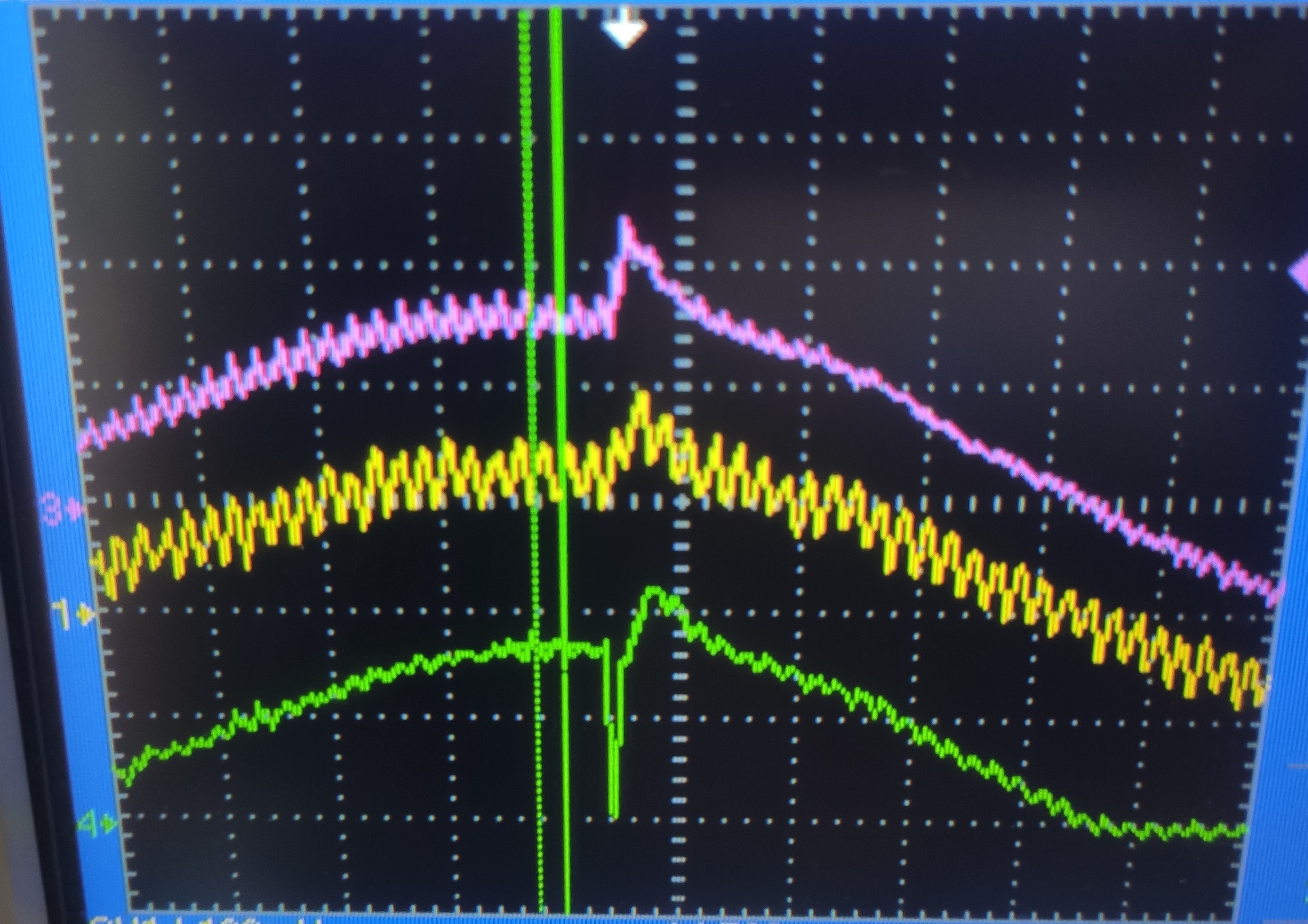
I probed analog voltage on B2 and C1 pins(input), but it is not having any fluctuations. So the input to ADC pin is not having glitch but converted Digital Result(observed on DSO by DAC module) is having a glitch. I am attaching the waveforms image below.

Yellow is the ADC pin input voltage. I am converting that ADC count into analog again by the DAC module. Note that, glitch stays for only one sampling time. (one-time conversion module is giving wrong digital counts)

Edit:

I am adding code for ADC configuration:

void InitADC()
{
    //Set Voltage reference for ADCA, ADCB and ADCC
    SetVREF(ADC_ADCA, ADC_INTERNAL, ADC_VREF3P3);   //VREF 3.3
    SetVREF(ADC_ADCC, ADC_INTERNAL, ADC_VREF3P3);   //VREF 3.3
    SetVREF(ADC_ADCB, ADC_INTERNAL, ADC_VREF3P3);   //VREF 3.3

    EALLOW;
    AdcaRegs.ADCCTL2.bit.PRESCALE = 6;              //Prescaler is 4  //systemclock is 100Mhz,ADC clock is 25Mhz
    AdcaRegs.ADCCTL1.bit.INTPULSEPOS = 1;           //Interrupt after Conversion
    AdcaRegs.ADCCTL1.bit.ADCPWDNZ = 1;              //Powerup ADC

    AdccRegs.ADCCTL2.bit.PRESCALE = 6;              //Prescaler is 4
    AdccRegs.ADCCTL1.bit.INTPULSEPOS = 1;           //Interrupt after Conversion
    AdccRegs.ADCCTL1.bit.ADCPWDNZ = 1;              //Powerup ADC

    AdcbRegs.ADCCTL2.bit.PRESCALE = 6;              //Prescaler is 4
    AdcbRegs.ADCCTL1.bit.INTPULSEPOS = 1;           //Interrupt after Conversion
    AdcbRegs.ADCCTL1.bit.ADCPWDNZ = 1;              //Powerup ADC

    EDIS;
    DELAY_US(1000);  //1 ms delay to setup supply

    //EOC5 of ADCA is Generating Interrupt by INT1SEL
    
    EALLOW;
    AdcaRegs.ADCSOC0CTL.bit.CHSEL = 0;     // SOC0 will convert pin A1
    AdcaRegs.ADCSOC0CTL.bit.ACQPS = 30;    // Sample window is 30 SYSCLK cycles
    AdcaRegs.ADCSOC0CTL.bit.TRIGSEL = 5;   // Trigger on ePWM1 SOCA

    AdcaRegs.ADCSOC1CTL.bit.CHSEL = 1;
    AdcaRegs.ADCSOC1CTL.bit.ACQPS = 30;
    AdcaRegs.ADCSOC1CTL.bit.TRIGSEL = 5;
  
    AdcaRegs.ADCSOC2CTL.bit.CHSEL = 2;
    AdcaRegs.ADCSOC2CTL.bit.ACQPS = 30;
    AdcaRegs.ADCSOC2CTL.bit.TRIGSEL = 5;

    AdcaRegs.ADCSOC4CTL.bit.CHSEL = 4;
    AdcaRegs.ADCSOC4CTL.bit.ACQPS = 30;
    AdcaRegs.ADCSOC4CTL.bit.TRIGSEL = 5;

    AdcaRegs.ADCSOC5CTL.bit.CHSEL = 5;
    AdcaRegs.ADCSOC5CTL.bit.ACQPS = 30;
    AdcaRegs.ADCSOC5CTL.bit.TRIGSEL = 5;

    AdcaRegs.ADCINTSEL1N2.bit.INT1SEL = 5; // End of SOC5 will set INT1 flag
    AdcaRegs.ADCINTSEL1N2.bit.INT1E = 1;   // Enable INT1 flag
    AdcaRegs.ADCINTFLGCLR.bit.ADCINT1 = 1; // INT1 flag is cleared

    AdcbRegs.ADCSOC1CTL.bit.CHSEL = 1;     
    AdcbRegs.ADCSOC1CTL.bit.ACQPS = 30;     
    AdcbRegs.ADCSOC1CTL.bit.TRIGSEL = 5;   

    AdcbRegs.ADCSOC2CTL.bit.CHSEL = 2;     
    AdcbRegs.ADCSOC2CTL.bit.ACQPS = 30;     
    AdcbRegs.ADCSOC2CTL.bit.TRIGSEL = 5;   

    AdcbRegs.ADCSOC3CTL.bit.CHSEL = 3;    
    AdcbRegs.ADCSOC3CTL.bit.ACQPS = 30;     
    AdcbRegs.ADCSOC3CTL.bit.TRIGSEL = 5;  

    AdccRegs.ADCSOC0CTL.bit.CHSEL = 0;    
    AdccRegs.ADCSOC0CTL.bit.ACQPS = 30;     
    AdccRegs.ADCSOC0CTL.bit.TRIGSEL = 5;   
    
    AdccRegs.ADCSOC1CTL.bit.CHSEL = 1;     
    AdccRegs.ADCSOC1CTL.bit.ACQPS = 30;     
    AdccRegs.ADCSOC1CTL.bit.TRIGSEL = 5;   
    
    AdccRegs.ADCSOC2CTL.bit.CHSEL = 3;     
    AdccRegs.ADCSOC2CTL.bit.ACQPS = 30;     
    AdccRegs.ADCSOC2CTL.bit.TRIGSEL = 5;   
    
    AdccRegs.ADCSOC3CTL.bit.CHSEL = 5;    
    AdccRegs.ADCSOC3CTL.bit.ACQPS = 30;     
    AdccRegs.ADCSOC3CTL.bit.TRIGSEL = 5;   

    AdccRegs.ADCSOC4CTL.bit.CHSEL = 14;
    AdccRegs.ADCSOC4CTL.bit.ACQPS = 30;
    AdccRegs.ADCSOC4CTL.bit.TRIGSEL = 5;

    EDIS;

}//InitADC

  • Hi,

    Could you please provide the code related to ADC configure, set-up and power-up?

    Thank you.

  • Hi Chirag,

    Do SOCs running in parallel use the same S+H duration (configured by the ACQPS SOC setting)? 

    What is the drive impedance and bandwidth for the signal conditioning circuits for these signals?  Is it different than the other channels? 

    Are any of the channels using PGAs?

    Is there any difference if you change the channel sampling order (by changing which SOCs map to which channels)?

    Are you sure the ADCCLK is 50MHz or less? 

    Does the glitch always occur in the same place in the waveform, or randomly?  Does it correspond to any other event in the system (e.g. communications interface sends or receives a message, ePWM switches, power stage reaches X power)?


  • I edited the question and added code. Please look at it.

  • Devin, Thanks for the quick response.

    1. Yes, SOC's running in parallel using the same S+H duration.

    2. I have another channel which uses the same drive Impedance and bandwidth but gives good result.

    3. I am not using PGA for any channel.

    4. I tried to change SOC and SOC order both. No improvement.

    5.ADC clock is 25 Mhz. I have attached the code. you can look at it and verify and suggest changes.

    6.No, it is not occurring at the same place in the waveform.

    7. For the last question, I would like to add a few more details,

    I am starting my ADC conversion by the PWM trip. I am using the up-down counter mode. I am starting conversion at zero and Maximum(period) count. So in one PWM cycle, I will be able to sample ADC twice. one at the starting of PWM and next in the middle of PWM.

    After End of Conversion, I will start my ADC ISR, where I will do calculations on ADC counts.

    I am also adding code for the 7th point, which starts ADC conversion at the start and top of the up-down counter.

    If My PWM frequency is X then my sampling frequency will be 2x and this glitch stays for only one sample period or 1/2X sampling time.

    I hope I made things clear enough. 

        EALLOW;
        EPwm1Regs.ETSEL.bit.SOCAEN = 1;        // Enable SOC on A group
        EPwm1Regs.ETSEL.bit.SOCASEL = 3;       //start conversion at zero and top count
        EPwm1Regs.ETPS.bit.SOCAPRD = 1;        // Generate pulse on 1st event
        EDIS;

  • Hi Chirag,

    Everything seems to be setup OK. 

    I would recommend that you use ADCCLK = 50MHz; there isn't any performance or power benefit to running the ADC slower than 50MHz.  I don't think this will help your specific issue though (unless there is some issue with running out of time to compute the ISR since this will reduce the time between trigger received and when the 5th result is ready). 

    If you don't need to do computations/control updates in both ISRs (both period and zero triggers) you can save an ISR by using "burst mode" to collect two sets of conversions into two sets of ADC result registers without using an intermediate ISR.  Don't worry about this until you solve the current issue.

    Additional debug options:

    • Can you permute which ADC channels the physical signals are connected to?  This might prove that the glitch is related to the input signal or the channel depending on if the glitch goes with the signal or the channel?
    • Can you capture all the ADC results into a buffer in RAM and then plot the results to see if the glitch is in the conversion results or only in the DAC output?  

  • Hii Devin,

    I tried above suggested debug options, but no lead.

    I sampled one voltage sample on adc pin and used 4 SOCs to use convert sample. All 4 SOC results have glitches but at different time. So I am doing average of all 4 to reduce effect of the same.

    So my question is if my input analog voltage is same then why converted digital counts are different(spike in one of four at a time). Problem in SOC unit? 

    I used another hardware board which is identical to first one doesn't have glitch. Is there any possibility of damage in MCU part?

    I will change MCU and update here too. 

  • Hi Chirag,

    Any update? Was switching the MCU able to resolve the issue?

    One test that you can do to determine if an ADC  input channel is damaged is to test the leakage current: source in 3.3V or 0V and observe the leakage current in/out of the device.  Inputs that have been damaged from ESD or EOS tend to exhibit leakage in the mA range which is an order of magnitude greater than the device spec' for pin leakage on most pins.