Other Parts Discussed in Thread: TMS570LS0332, , C2000WARE
Tool/software: Code Composer Studio
Hi I am having an issue with SPI communication between 2 microcontrollers one is the DSP in the TMS320F280049 as slave and the master is TMS570LS0332. I am thinking that I may be doing something wrong in the DSP configuration since when I check the data sent by the master in the oscilloscope the signal seems correct, however the data in the DSP is wrong, in some cases it is shifted by one.
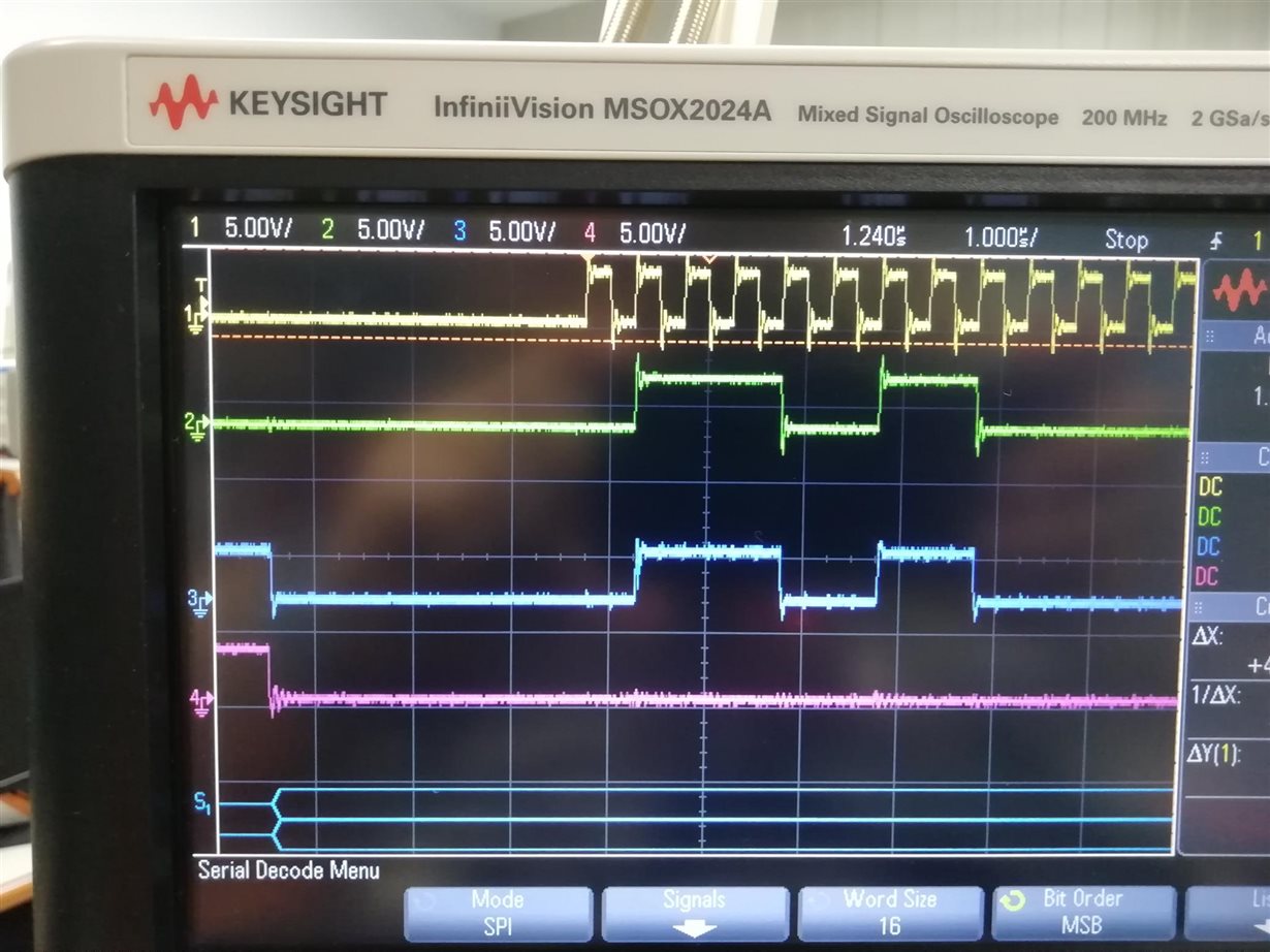
- Channel 1 is the clock signal
- Channel 2 is the Master with the first word = 0x7301
- Channel 3 is the slave and the response should be 0x7301 as well however it sends 0x7302 (the first byte seems ok the second in the response is corrupted, in this sample, it cannot be seen in the image)
- Channel 4 is the CS signal, in master SPI I added a delay at the beginning and at the end.
Master SPI is configured as follows:
void mibspiInit(void)
{
    U32 i;
    U32  regTestFLG;

    // Initialize MibSPI1
    // $$ Start mibSPI 1 Initialization
    /** bring MIBSPI out of reset */
    mibspiREG1->GCR0 = 0U; // nRESET = in reset
    mibspiREG1->GCR0 = 1U; // nRESET = out of reset

    /** enable MIBSPI1 multibuffered mode and enable buffer RAM */
    mibspiREG1->MIBSPIE = (mibspiREG1->MIBSPIE & 0xFFFFFFFEU) // RXRAM ACCESS = unchanged
                        | MIBSPIE_MSPIENA_CONFIG;

    /** MIBSPI1 master mode and clock configuration */
    mibspiREG1->GCR1 = (mibspiREG1->GCR1 & 0xFFFFFFFCU) // remaining fields = unchanged
                     | MIBSPI_GCR1_CLKMOD_CONFIG
                     | MIBSPI_GCR1_MASTER_CONFIG;

    /** MIBSPI1 enable pin configuration */
    mibspiREG1->INT0 = (mibspiREG1->INT0 & 0xFEFFFFFFU) // remaining fields = unchanged
                     | INT0_ENABLEHIGHZ_CONFIG;

    /** - Delays */
    mibspiREG1->DELAY = MIBSPI_DELAY_CONFIG;

    /** - Data Format 0 */
    mibspiREG1->FMT0 = MIBSPI_FTM0_CONFIG;

    /** - Data Format 1 */
    mibspiREG1->FMT1 = MIBSPI_FTM1_CONFIG;

    /** - Data Format 2 */
    mibspiREG1->FMT2 = MIBSPI_FTM2_CONFIG;

    /** - Data Format 3 */
    mibspiREG1->FMT3 = MIBSPI_FTM3_CONFIG;

    /** - Default Chip Select */
    mibspiREG1->DEF = MIBSPI_DEF_CONFIG;

    // Set fault in UI RAM in case the following loop cause a WDT timeout
    uirSaveFault.bit.mcuSbitFault = TRUE;

    /** - wait for buffer initialization complete before accessing MibSPI registers */
    regTestFLG = mibspiREG1->FLG;
    while ((regTestFLG & 0x01000000U) != 0U)
    {
        // Loop here until a WDT timeout/reset at which time the exception will be reported.
        regTestFLG = mibspiREG1->FLG;
    }

    // Clear fault in UI RAM - loop did not cause a WDT timeout
    uirSaveFault.bit.mcuSbitFault = FALSE;

    /** enable MIBSPI RAM Parity */
    mibspiREG1->UERRCTRL = (mibspiREG1->UERRCTRL & 0xFFFFFFF0U) // PTESTEN = unchanged
                         | (MIBSPI_EDEN_CONFIG);

    // $$ Common Initialization for mibSPI 1 TGs
    /** - initialize transfer groups */
    mibspiREG1->TGCTRL[0U] = TGCTRL0_CONFIG;

    mibspiREG1->TGCTRL[1U] = TGCTRL1_CONFIG;

    mibspiREG1->TGCTRL[2U] = TGCTRL2_CONFIG;

    mibspiREG1->TGCTRL[3U] = TGCTRL3_CONFIG;

    mibspiREG1->TGCTRL[4U] = TGCTRL4_CONFIG;

    mibspiREG1->TGCTRL[5U] = TGCTRL5_CONFIG;

    mibspiREG1->TGCTRL[6U] = TGCTRL6_CONFIG;

    mibspiREG1->TGCTRL[7U] = TGCTRL7_CONFIG;

    mibspiREG1->LTGPEND = (mibspiREG1->LTGPEND & 0xFFFF00FFU)           // remaining fields = unchanged
                        | LTGPEND_LPEND_CONFIG;

    /** - initialize buffer ram */
    i = 0U;

    // $$ AC9-3142 - Initialize mibSPI 1 TG0
    // Initialize Transfer Group 0 control words
    while (i < (32U-1U))
    {
        mibspiRAM1->tx[i].control = MIBSPI_CONTROL_CONFIG;
        i++;
    }
    // Initialize Transfer Group 0 control word for last buffer
    mibspiRAM1->tx[i].control = MIBSPI_CONTROL_LAST_CONFIG;


    // $$ Finalize mibSPI 1 Initialization
    /** - set interrupt levels */
    mibspiREG1->LVL = MIBSPI_LVL_CONFIG;

    /** - clear any pending interrupts */
    mibspiREG1->FLG |= 0xFFFFU;  // Clear all nFLG interrupt flags
                                 // Note: writing to BUFINITACTIVE has no effect

    /** - set interrupt enables */
    mibspiREG1->INT0 = (mibspiREG1->INT0 & 0xFFFF0000U);  // Disable all nENA interrupts

    /** - MIBSPI1 Port initial output values */
    mibspiREG1->PC3 =  MIBSPI_PC3_CONFIG;

    /** - MIBSPI1 Port direction */
    mibspiREG1->PC1 =  MIBSPI_PC1_CONFIG;

    /** - MIBSPI1 Port open drain enable */
    mibspiREG1->PC6 =  MIBSPI_PC6_CONFIG;              // PDR = disable for all pins

    /** - MIBSPI1 Port pullup / pulldown selection */
    mibspiREG1->PC8 = MIBSPI_PC8_CONFIG;

    /** - MIBSPI1 Port pullup / pulldown enable*/
    mibspiREG1->PC7 =  MIBSPI_PC7_CONFIG;

    /** MIBSPI1 set pins to functional */
    mibspiREG1->PC0 =  MIBSPI_PC0_CONFIG;

    /** - Finally start MIBSPI1 */
    mibspiREG1->GCR1 = (mibspiREG1->GCR1 & 0xFEFFFFFFU) // remaining fields = unchanged
                     | MIBSPI_GCR1_SPIEN_CONFIG;
}
Slave SPI is configured as follows:
static void initSpiASlave(void)
{
    U16 regValue;

    // Must put SPI into reset before configuring it (disable SPI A module)
    //
    spiAREG1->SPI_O_CCR &= ~(SPI_CCR_SPISWRESET);

    //
    // Set polarity and data width.
    //
    regValue = 0U   << 6U  // CLKPOLARITY = 0U -> Data is output on rising edge and input on falling edge.
            |  0U   << 5U  // HS_MODE = disabled
            |  0xFU;       // SPICHAR = 16-bit word


    spiAREG1->SPI_O_CCR = (spiAREG1->SPI_O_CCR & 0xFF90) | regValue;

    //
    // Set the mode and phase.
    //
    regValue = 0U   << 4U  // OVERRUNINTENA = disabled
            |  0U   << 3U  // CLK_PHASE = Normal SPI clocking scheme
            |  0U   << 2U  // MASTER_SLAVE = Slave
            |  1U   << 1U  // TALK = enabled (slave sends data to master)
            |  0U;         // SPIINTENA = interrupt is enabled

    spiAREG1->SPI_O_CTL = (spiAREG1->SPI_O_CTL & 0xFFE0) | regValue;

    //
    // Enable the FIFO.
    //
    regValue = 0U  << 15U  // 0h (R/W) = Write 0 to reset the SPI transmit and receive channels
            |  0U  << 14U  // SPIFFENA = enhancements disabled
            |  1U  << 13U  // TXFIFO = Release transmit FIFO from reset
            |  0U  << 5U;  // TXFFIENA = FIFO interrupt disabled

    spiAREG1->SPI_O_FFTX = (spiAREG1->SPI_O_FFTX & 0x1FDF) | regValue;

    regValue = 1U  << 14U  // RXFFOVFCLR = clear SPIFFRX[RXFFOVF]
            |  1U  << 13U  // RXFIFORESET = Re-enable receive FIFO operation
            |  0U  << 5U;  // RXFFIENA = receive FIFO interrupt disabled

    spiAREG1->SPI_O_FFRX = (spiAREG1->SPI_O_FFRX & 0x9FDF) | regValue;

    spiAREG1->SPI_O_FFTX |= 1U  << 15U;  // 1h (R/W) = SPI FIFO can resume transmit or receive.

    //
    // Configuration complete. Enable the module.
    //
    spiAREG1->SPI_O_CCR |= SPI_CCR_SPISWRESET;
}
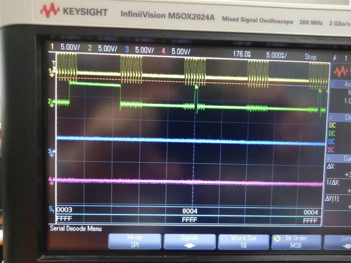
Also, I used an aardvark to send data at the same rate (2 MHz) and DSP recognizes data correctly, the difference between both signals is that there is a gap between FIFO transfers of 8 bits, the master controller has no gaps it sends the 32 bytes as a single message with no gaps between:
Is there any limitation on the DSP SPI that I am not considering?
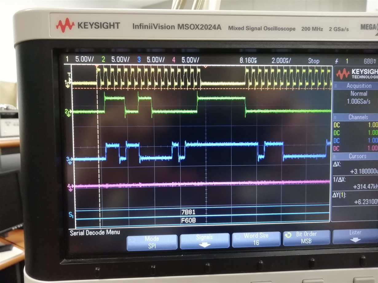
After reconfiguring mibSPI on master side, I managed to enter a gap between ever word (16 bits) transfer:
Note that mibSPI enters gaps between every 16 bits while aardvark does between every 8 bits, aardvark data is correctly recognized in DSP side, however mibSPI data is all corrupted... I think there might be a timing limitation in FIFO mode that is not mentioned in the data sheet.


