Part Number: TMS320F280049C
Other Parts Discussed in Thread: C2000WARE
Hi All,
I am using microcontroller F280049C. I need to configure more parameters (TBPRD, TBPHS, CMPA, DBRED, DBFED) into more ePWM modules (ePWM1, ePWM2, ePWM3). I need to set all shadow registers and then load them all to active at the same time. Ideally when counters are at zero.
It works well when I just configure all shadow registers events to load new value at counter zero. However there is still a hazard when counter zero occurs in the middle of changing register values. Therefore I need to use global load in one shot mode. I configure all registers to be synchronized:
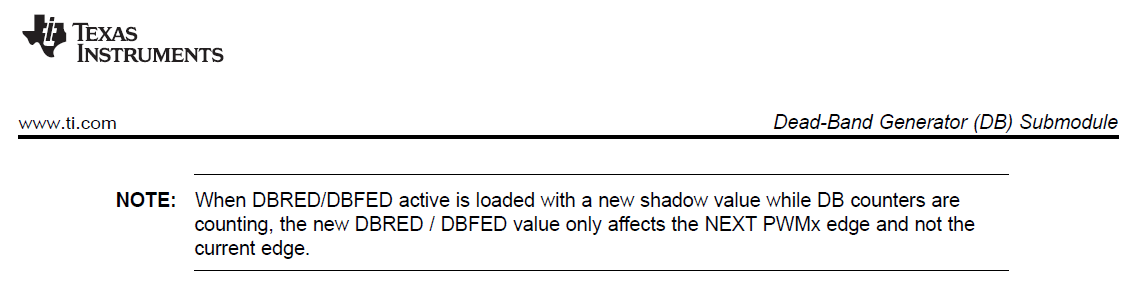
I have problem that loading DBRED, DBFED happens one counter cycle before also TBPRD is updated. I can’t find such issue documented in reference manual or errata. Here is what I do:
#define SYNCED_REGS ((uint16_t)(EPWM_GL_REGISTER_TBPRD_TBPRDHR | EPWM_GL_REGISTER_CMPA_CMPAHR | EPWM_GL_REGISTER_CMPB_CMPBHR | EPWM_GL_REGISTER_CMPC | EPWM_GL_REGISTER_CMPD | EPWM_GL_REGISTER_DBRED_DBREDHR | EPWM_GL_REGISTER_DBFED_DBFEDHR | EPWM_GL_REGISTER_AQCSFRC))
I also use EPWMXLINK to synchronize some registers among different ePWM modules.
The problem occurs when I change DBFED, DBRED times and also TBPRD at the same time. Here is what I get:
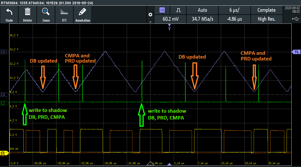
Green – TBPRD Counter value
Yellow – time when trigger one shot load GLDCTL2.bit.OSHTLD = 1
Red – ePWM1A
Blue – ePWM1B
Yellow arrow points to the moment when I change TBPRD and DBFED, DBRED to higher values. Then I trigger one shot load. As we can see the FED and RED are loaded to active when counter reach zero for the first time, but the TBPRD is set at next counter zero.
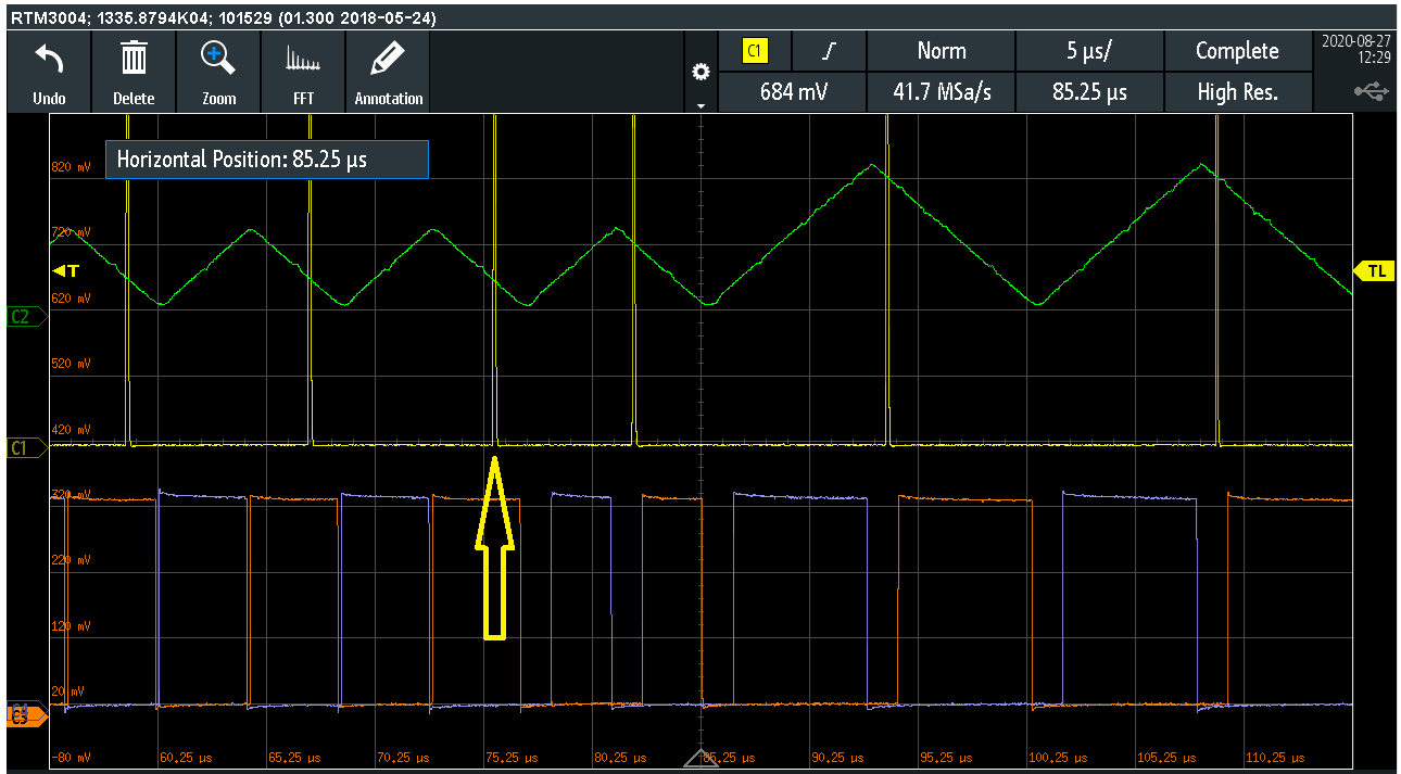
The same thing happens when I do it other way around:

I am attaching ePWM register values from debuger.
Could you please advice what am I doing wrong?
Thank you in advance.
Best Regards,
Juraj