This thread has been locked.

If you have a related question, please click the "Ask a related question" button in the top right corner. The newly created question will be automatically linked to this question.

TMS320F280049C: layout guidelines

Part Number: TMS320F280049C

hi,

we are using F280049CRSHS uP and would appreciate some hints about routing Crystal Oscilator and decoupling caps.

Generally it seems the F280049CRSHS  does not have comfortable pin arrangement in terms of placing decoupling caps - no GND pins adjacent to VDD/VDDIO.

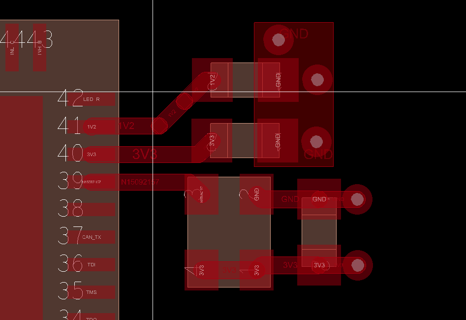
What we did is to connect VDD pad of decoupling cap directly to pin and GND pad by via to thermal pad. Is that ok?

About Oscillator Connection - does it look good? - again pin arrangement does not facilitate to make guard GND ring around it.

layout

thanks a lot in advance

have a great day

KR

Vincenzo

  • Vincenzo, 

    Often times the decoupling caps have to go through a Via to get to ground, this is OK. In many of our example designs we actually place them on the back of the board. Remember that the distance that the signal travels through the board on a VIA also counts. The typical board thickness is about 62mil, so if you can place a component only on the top layer and avoid going through the board that can be better. In this case it is OK to use a via.

    Adding a guard ring is good practice, but we have not seen it to be necessary for our devices. Keep the traces short and clean. It looks like your design does this, so you shouldn't have and issues.

    Regards,
    Cody