This thread has been locked.

If you have a related question, please click the "Ask a related question" button in the top right corner. The newly created question will be automatically linked to this question.

TMS320F280049: SPI communication with ADS1248

Part Number: TMS320F280049
Other Parts Discussed in Thread: ADS1248, C2000WARE, ADS1298

Hi Team,

I am afraid this might me be a long question. Anyway I will make it as short as possible. I am trying to establish communication between 280049 and ADS1248. I am experiencing following issues while doing the same.

1. At first I was not using FIFO and not monitoring DRDY pin for data conversion completion indication. Instead I used an appropriate delay of 201 milli seconds (5SPS) in between SYNC command and RDATA command to read conversion result from ADC. While doing like this I was not able read correct results from ADC. I probed my SPI pins in this condition and observed that instead of a series of data I am having only the first data (0x1640) appearing on my SIMO pin and after that SIMO pin stays at high state irrespective of any data written to transmit buffer. 

        SpiaRegs.SPITXBUF                   = 0xFF06; // Send the RESET command and wait for 0.6ms
        DELAY_US(600);

     // Register configuration of ADS1248

        SpiaRegs.SPITXBUF                   = 0x1640; // Send the SDATAC command and WREG Command 1st byte
        SpiaRegs.SPITXBUF                   = 0x030A; // WREG Command 2nd byte and MUX0 register value
        SpiaRegs.SPITXBUF                   = 0x0020; // VBIAS register value and MUX1 register value
        SpiaRegs.SPITXBUF                   = 0x404A; // SYS0 register and WREG 1st command byte
        SpiaRegs.SPITXBUF                   = 0x0105; // WREG 2nd command byte and IDAC0 register value
        SpiaRegs.SPITXBUF                   = 0x0304; // IDAC1 register value and NOP command

My SPI baud rate is at 1MHz and system clock frequency is at 100MHz. Considering ADS1248 is a slow slave I started to add delay in between each transfer that is in between each write to spi transmit buffer. With trial and error I got expected results with a delay of 20 micro seconds in between each transfer.

        SpiaRegs.SPITXBUF                   = 0xFF06; // Send the RESET command and wait for 0.6ms
        DELAY_US(600);

     // Register configuration of ADS1248

        SpiaRegs.SPITXBUF                   = 0x1640; // Send the SDATAC command and WREG Command 1st byte
        DELAY_US(20);
        SpiaRegs.SPITXBUF                   = 0x030A; // WREG Command 2nd byte and MUX0 register value
        DELAY_US(20);
        SpiaRegs.SPITXBUF                   = 0x0020; // VBIAS register value and MUX1 register value
        DELAY_US(20);
        SpiaRegs.SPITXBUF                   = 0x404A; // SYS0 register and WREG 1st command byte
        DELAY_US(20);
        SpiaRegs.SPITXBUF                   = 0x0105; // WREG 2nd command byte and IDAC0 register value
        DELAY_US(20);
        SpiaRegs.SPITXBUF                   = 0x0304; // IDAC1 register value and NOP command
        DELAY_US(20);

With this code everything was working fine but I can't have this much delay in my code due to other limitations. Why this delay is required? anything less than 20 micro seconds is not working. 

2. Since I was was facing issues with Non FIFO transfer I attempted to transmit data using FIFO but without any interrupts. Using FIFO I am able to send data correctly through SIMO without delay. Since it is a duplex transmission I considered resetting receive FIFO pointer to zero before receiving my conversion results. When I wrote code like the following resetting FIFO it doesn't resetting the FIFO. 

SpiaRegs.SPITXBUF                   = 0xFF12; // NOP and RDATA
SpiaRegs.SPIFFRX.bit.RXFIFORESET    = 0; 
SpiaRegs.SPIFFRX.bit.RXFIFORESET    = 1;

But when I wrote the code like the following It is actually resetting the FIFO. Why this happens?

SpiaRegs.SPIFFRX.bit.RXFIFORESET    = 0;
SpiaRegs.SPITXBUF                   = 0xFF12; // NOP and RDATA
SpiaRegs.SPIFFRX.bit.RXFIFORESET    = 1;

3. Even if I successfully cleared FIFO I am sending only 32 clock cycles to get 4 bytes of data that is 2 FIFO inputs (2 bytes of each). Instead of 2 data each of 2 byte the FIFOSTS is showing 4 data inside FIFO. From where the extra two data coming from? Is there is any provision to look into FIFO memory location to actually observe the stack manually?

SpiaRegs.SPIFFRX.bit.RXFIFORESET    = 0;
SpiaRegs.SPITXBUF                   = 0xFF12; // NOP and RDATA
SpiaRegs.SPIFFRX.bit.RXFIFORESET    = 1;
SpiaRegs.SPITXBUF                   = 0xFFFF; // NOP commands to receive first 2 bytes of data
SpiaRegs.SPITXBUF                   = 0xFFFF; // NOP commands to receive second 2 bytes of data
while(SpiaRegs.SPIFFRX.bit.RXFFST < 4); // RXFFST is 4 here instead of 2

I am attaching total full code along with this.

/* EXTERNAL CRYSTAL FREQUENCY 20MHz

*******************************************************************************/
//-----------------------------------------------------------------------------
// Include Header Files
// ----------------------------------------------------------------------------


#include"F28x_Project.h"

void main()
{
    int32 r1 = 0x00000000,r3 = 0x00000000;
    int16 r2 = 0x0000;

// Initiate system controls, GPIO pins, interrupt

    InitSysCtrl();
    InitGpio();

    EALLOW;

        GpioCtrlRegs.GPAGMUX1.bit.GPIO9     = 1;
        GpioCtrlRegs.GPAMUX1.bit.GPIO9      = 3; // set Gpio pin 9 as SPI clock pin
        GpioCtrlRegs.GPAPUD.bit.GPIO9       = 0; // Pull up enable
        GpioCtrlRegs.GPAQSEL1.bit.GPIO9     = 3; // Qualifier Selection

        GpioCtrlRegs.GPAGMUX1.bit.GPIO8     = 1;
        GpioCtrlRegs.GPAMUX1.bit.GPIO8      = 3; // set Gpio pin 8 as SPI SIMO pin
        GpioCtrlRegs.GPAPUD.bit.GPIO8       = 0; // Pull up enable
        GpioCtrlRegs.GPAQSEL1.bit.GPIO8     = 3; // Qualifier Selection

        GpioCtrlRegs.GPAGMUX1.bit.GPIO10    = 1;
        GpioCtrlRegs.GPAMUX1.bit.GPIO10     = 3; // set Gpio pin 10 as SPI SOMI pin
        GpioCtrlRegs.GPAPUD.bit.GPIO10      = 0; // Pull up enable
        GpioCtrlRegs.GPAQSEL1.bit.GPIO10    = 3; // Qualifier Selection

        GpioCtrlRegs.GPAGMUX1.bit.GPIO14    = 0;
        GpioCtrlRegs.GPAMUX1.bit.GPIO14     = 0; // set Gpio pin 14 as GPIO output pin (CS/)
        GpioCtrlRegs.GPADIR.bit.GPIO14      = 1; // set direction as output

        GpioCtrlRegs.GPAGMUX1.bit.GPIO15    = 0;
        GpioCtrlRegs.GPAMUX1.bit.GPIO15     = 0; // set Gpio pin 15 as GPIO output pin (START)
        GpioCtrlRegs.GPADIR.bit.GPIO15      = 1; // set direction as output

        GpioCtrlRegs.GPBGMUX1.bit.GPIO34    = 0;
        GpioCtrlRegs.GPBMUX1.bit.GPIO34     = 0; // set Gpio pin 34 as GPIO output pin (ADC_RST)
        GpioCtrlRegs.GPBDIR.bit.GPIO34      = 1; // set direction as output (ADC_RST)

    EDIS;

        GpioDataRegs.GPACLEAR.bit.GPIO15    = 1; // START pin LOW
        GpioDataRegs.GPASET.bit.GPIO14      = 1; // Clear CS/ pin to high
        GpioDataRegs.GPBSET.bit.GPIO34      = 1; // ADC Reset disabled

//        SpiaRegs.SPIFFTX.all                = 0xE040;
//        SpiaRegs.SPIFFRX.all                = 0x2044;
//        SpiaRegs.SPIFFCT.all                = 0x0;


        SpiaRegs.SPIFFTX.bit.SPIFFENA       = 1; // Enable FIFO mode
        SpiaRegs.SPIFFTX.bit.TXFFINTCLR     = 1;
        SpiaRegs.SPIFFTX.bit.TXFIFO         = 1;
        SpiaRegs.SPIFFTX.bit.SPIRST         = 1;
        SpiaRegs.SPIFFRX.bit.RXFFOVFCLR     = 1;
        SpiaRegs.SPIFFRX.bit.RXFFINTCLR     = 1;
        SpiaRegs.SPIFFRX.bit.RXFIFORESET    = 1;

        SpiaRegs.SPICCR.bit.SPISWRESET      = 0; // clear software reset bit
        SpiaRegs.SPICTL.bit.MASTER_SLAVE    = 1; // master mode selected
        SpiaRegs.SPICTL.bit.CLK_PHASE       = 0; // clock phase selection
        SpiaRegs.SPICCR.bit.CLKPOLARITY     = 0; // clock polarity
        SpiaRegs.SPIBRR.bit.SPI_BIT_RATE    = 24; //(25MHz/25 = 1 MHz)
        SpiaRegs.SPICCR.bit.SPICHAR         = 15; // character per transfer
        SpiaRegs.SPISTS.bit.INT_FLAG        = 1; // clear interrupt flag
        SpiaRegs.SPISTS.bit.OVERRUN_FLAG    = 1; // clear over run flag
        SpiaRegs.SPIPRI.bit.FREE            = 1;
        SpiaRegs.SPICCR.bit.SPILBK          = 0; // loop back disable
        SpiaRegs.SPICTL.bit.TALK            = 1; // slave talk enabled
        SpiaRegs.SPICTL.bit.SPIINTENA       = 0; // interrupt disable
        SpiaRegs.SPICCR.bit.SPISWRESET      = 1; // software reset disabled
        
        GpioDataRegs.GPACLEAR.bit.GPIO14    = 1; // Clear CS/ pin to low
        GpioDataRegs.GPASET.bit.GPIO15      = 1; // Enable the device by setting START pin high
        DELAY_US(1);
        SpiaRegs.SPIFFRX.bit.RXFIFORESET    = 0;
        SpiaRegs.SPITXBUF                   = 0xFF06; // Send the RESET command and wait for 0.6ms
        DELAY_US(600);

     // Register configuration of ADS1248

        SpiaRegs.SPITXBUF                   = 0x1640; // Send the SDATAC command and WREG Command 1st byte
        SpiaRegs.SPITXBUF                   = 0x030A; // WREG Command 2nd byte and MUX0 register value
        SpiaRegs.SPITXBUF                   = 0x0020; // VBIAS register value and MUX1 register value
        SpiaRegs.SPITXBUF                   = 0x404A; // SYS0 register and WREG 1st command byte
        SpiaRegs.SPITXBUF                   = 0x0105; // WREG 2nd command byte and IDAC0 register value
        SpiaRegs.SPITXBUF                   = 0x0304; // IDAC1 register value and NOP command
//        GpioDataRegs.GPACLEAR.bit.GPIO15    = 1; // START pin held low
//        while(SpiaRegs.SPIFFTX.bit.TXFFST !=0);
        GpioDataRegs.GPASET.bit.GPIO14      = 1; // Clear CS/ pin to high

        DELAY_US(201000);

        GpioDataRegs.GPACLEAR.bit.GPIO14    = 1; // Clear CS/ pin to low
        DELAY_US(1);

        SpiaRegs.SPITXBUF                   = 0xFF12; // NOP and RDATA
        SpiaRegs.SPIFFRX.bit.RXFIFORESET    = 1;
        SpiaRegs.SPITXBUF                   = 0xFFFF; // NOP commands
        SpiaRegs.SPITXBUF                   = 0xFFFF; // NOP commands
        while(SpiaRegs.SPIFFRX.bit.RXFFST < 4);
        r1                                  = SpiaRegs.SPIRXBUF;
        r2                                  = SpiaRegs.SPIRXBUF;
        r2                                  = SpiaRegs.SPIRXBUF;
        r2                                  = SpiaRegs.SPIRXBUF;
        r3                                  = (r1<<8)+(r2>>8);
        DELAY_US(1);
        GpioDataRegs.GPASET.bit.GPIO14      = 1; // Clear CS/ pin to high

}


Thank you,

Vineeth N

  • Hi Vineeth,

    Vineeth N said:
    With this code everything was working fine but I can't have this much delay in my code due to other limitations. Why this delay is required? anything less than 20 micro seconds is not working. 

    This is happening because you are essentially overwriting the data in the shift register while the SPI is shifting out data. Keep in mind that the CPU is running much faster than the SPI. The correct sequence is for you to check the BUFFULL_FLAG bit in the STS register to ensure there is no character being transmitted before you write a new character.

    Vineeth N said:
    Since I was was facing issues with Non FIFO transfer I attempted to transmit data using FIFO but without any interrupts. Using FIFO I am able to send data correctly through SIMO without delay.

    When FIFO is enabled, the CPU can write up to 16 characters to the SPI without overwriting the data in the SPI shift register. It is still good practice to check the TXFFST bits in the SPIFFTX register to make sure the FIFO is not full before writing a new character.

    Vineeth N said:
    But when I wrote the code like the following It is actually resetting the FIFO. Why this happens?

    I think you have the same problem where you are resetting FIFO in the middle of a character transmission. Again, keep in mind that the SPI is running slower than the CPU. When you write a values to SPITXBUF, it will take several microseconds for the data to get shifted out. However, in your code you have the CPU immediately reset the FIFO.

    Vineeth N said:
    3. Even if I successfully cleared FIFO I am sending only 32 clock cycles to get 4 bytes of data that is 2 FIFO inputs (2 bytes of each). Instead of 2 data each of 2 byte the FIFOSTS is showing 4 data inside FIFO. From where the extra two data coming from? Is there is any provision to look into FIFO memory location to actually observe the stack manually?

    I'm actually not clear on what your question here. Maybe you could re-phrase?

  • Hi Gus,

    Thanks for your response.

    Gus Martinez said:
    When FIFO is enabled, the CPU can write up to 16 characters to the SPI without overwriting the data in the SPI shift register. It is still good practice to check the TXFFST bits in the SPIFFTX register to make sure the FIFO is not full before writing a new character.

    When I used FIFO for transmitting I haven't seen any activity on FIFO transmit registers. All the register values are at zero all the times. I put a break point in the code after four successive writes to SPI transmit buffer and observed the value of TXFFST. It is found to be zero. This is wrong I think, What is your opinion on this?

    Gus Martinez said:
    I think you have the same problem where you are resetting FIFO in the middle of a character transmission. Again, keep in mind that the SPI is running slower than the CPU. When you write a values to SPITXBUF, it will take several microseconds for the data to get shifted out. However, in your code you have the CPU immediately reset the FIFO.

    I will check this and get back to you soon.

    Gus Martinez said:
    I'm actually not clear on what your question here. Maybe you could re-phrase?

    Of-course. What I meant to say is that after I reset the RXFFST to zero, I am expecting only two words from the slave to which I am communicating (ADS1248). I am giving instruction to read only two words from the slave (two NOP commands 0xFFFF for two word transfer). But what I am getting is, actually three words in FIFO instead of two. RXFFST showing 3 instead of 2. From where the extra one word is coming, this was my question.

    Thank you,

    Vineeth N

  • Vineeth,

    Vineeth N said:
    When I used FIFO for transmitting I haven't seen any activity on FIFO transmit registers. All the register values are at zero all the times. I put a break point in the code after four successive writes to SPI transmit buffer and observed the value of TXFFST. It is found to be zero. This is wrong I think, What is your opinion on this?

    That doesn't sound right. Do you see activity on the MOSI pin? 

    Make sure you are enabling the TX FIFO correctly. You can refer to the example code in C2000Ware. Specifically look at this example:

    C:\ti\c2000\C2000Ware_3_02_00_00\device_support\f28004x\examples\spi

    Another reference is the SPI example in the driverlib (also part of C2000Ware):

    C:\ti\c2000\C2000Ware_3_02_00_00\driverlib\f28004x\examples\spi\spi_ex1_loopback.c

    The source for the driverlib functions is located here:

    C:\ti\c2000\C2000Ware_3_02_00_00\driverlib\f28004x\driverlib\spi.h & spi.c

    Vineeth N said:
    Of-course. What I meant to say is that after I reset the RXFFST to zero, I am expecting only two words from the slave to which I am communicating (ADS1248). I am giving instruction to read only two words from the slave (two NOP commands 0xFFFF for two word transfer). But what I am getting is, actually three words in FIFO instead of two. RXFFST showing 3 instead of 2. From where the extra one word is coming, this was my question.

    Ok, here keep in mind that the SPI has a single shift register. When you load a character for TX, the SPI will shift the charater in, and simultaneously shift a character in. So, if you transmit two characters, you will also receive two characters. In most cases, you can read & discard those characters from the RX register. 

  • Hi Gus,

    Gus Martinez said:
    Make sure you are enabling the TX FIFO correctly.

    I think I have done this correctly. Anyway following is my settings for FIFO.

            SpiaRegs.SPIFFTX.bit.SPIRST         = 1; // SPI Reset. SPI FIFO can resume transmit or receive. No effect to the SPI registers bits.
            SpiaRegs.SPIFFTX.bit.SPIFFENA       = 1; // SPI FIFO Enhancements Enable
            SpiaRegs.SPIFFTX.bit.TXFIFO         = 1; // Release transmit FIFO from reset.
            SpiaRegs.SPIFFTX.bit.TXFFINTCLR     = 1; // TXFIFO Interrupt Clear. Write 1 to clear SPIFFTX[TXFFINT] flag
            SpiaRegs.SPIFFTX.bit.TXFFIENA       = 0; // TX FIFO interrupt based on TXFFIL match (less than or equal to) will be disabled.
            SpiaRegs.SPIFFTX.bit.TXFFIL         = 0; // A TX FIFO interrupt request is generated when there are no words remaining in the TX buffer
            SpiaRegs.SPIFFRX.bit.RXFFOVFCLR     = 1; // Receive FIFO Overflow Clear. Write 1 to clear SPIFFRX[RXFFOVF].
            SpiaRegs.SPIFFRX.bit.RXFIFORESET    = 1; // Re-enable receive FIFO operation.
            SpiaRegs.SPIFFRX.bit.RXFFINTCLR     = 1; // Receive FIFO Interrupt Clear. Write 1 to clear SPIFFRX[RXFFINT] flag
            SpiaRegs.SPIFFRX.bit.RXFFIENA       = 1; // RX FIFO interrupt based on RXFFIL match (greater than or equal to) will be disabled.

    I am not enabling the transmit FIFO interrupt, because I only want to observe TXFFINT flag to check whether the TXFIFO is empty or not. Only after making sure that the FIFO is empty I can disable the chip select line to slave or it will result in communication failure. That is my slave ADC will not receive data and get configured properly if I am removing chip select before a complete transmission. 

    To make sure the FIFO is empty my idea was to observe for TXFFINT flag. Since the TXFFIL is set to ZERO the interrupt flag will be set when there is no word available in TXFIFO. So I observed TXFFINT like in this,

            SpiaRegs.SPITXBUF                   = 0xFF06; // Send the RESET command and wait for 0.6ms
    
            while (SpiaRegs.SPIFFTX.bit.TXFFINT !=1 ); // Wait until TXFIFO is empty
            SpiaRegs.SPIFFTX.bit.TXFFINTCLR     = 1; // TXFIFO Interrupt Clear. Write 1 to clear SPIFFTX[TXFFINT] flag
    
            DELAY_US(600);
    
        // Register configuration of ADS1248
    
            SpiaRegs.SPITXBUF                   = 0x1640; // Send the SDATAC command and WREG Command 1st byte
            SpiaRegs.SPITXBUF                   = 0x030A; // WREG Command 2nd byte and MUX0 register value
            SpiaRegs.SPITXBUF                   = 0x0020; // VBIAS register value and MUX1 register value
            SpiaRegs.SPITXBUF                   = 0x444A; // SYS0 register and WREG 1st command byte
            SpiaRegs.SPITXBUF                   = 0x0105; // WREG 2nd command byte and IDAC0 register value
            SpiaRegs.SPITXBUF                   = 0x0304; // IDAC1 register value and NOP command
    
            while (SpiaRegs.SPIFFTX.bit.TXFFINT !=1 ); // Wait until TXFIFO is empty
            SpiaRegs.SPIFFTX.bit.TXFFINTCLR     = 1; // TXFIFO Interrupt Clear. Write 1 to clear SPIFFTX[TXFFINT] flag
    
    //        while(SpiaRegs.SPIFFRX.bit.RXFFST < 7 );
    
            DELAY_US(2);
            GpioDataRegs.GPASET.bit.GPIO14      = 1; // Clear CS/ pin to high

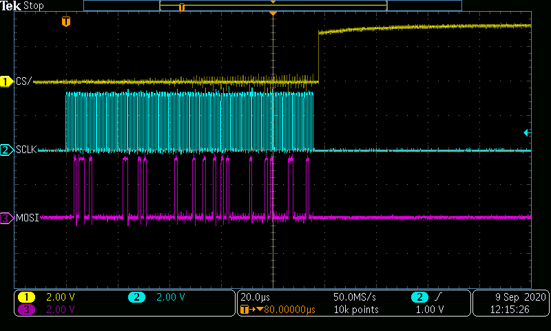
    And I got this scope shot.

    Here as we can see the chip select (CS/) goes high before the transmission completion. It is actually going HIGH even before first data through MOSI. 

    Gus Martinez said:
    Do you see activity on the MOSI pin? 

    As you can see the data is appearing on MOSI pin and it is the same data which I am sending. Since the CS/ is gone HIGH before the transmission the slave fails to accept the data. 

    When I tried the other way that is using RXFFST status to check for transmission completion, It is worked quite well. Following is my code

            SpiaRegs.SPITXBUF                   = 0xFF06; // Send the RESET command and wait for 0.6ms
    
    //        while (SpiaRegs.SPIFFTX.bit.TXFFINT !=1 ); // Wait until TXFIFO is empty
    //        SpiaRegs.SPIFFTX.bit.TXFFINTCLR     = 1; // TXFIFO Interrupt Clear. Write 1 to clear SPIFFTX[TXFFINT] flag
    
            DELAY_US(600);
    
        // Register configuration of ADS1248
    
            SpiaRegs.SPITXBUF                   = 0x1640; // Send the SDATAC command and WREG Command 1st byte
            SpiaRegs.SPITXBUF                   = 0x030A; // WREG Command 2nd byte and MUX0 register value
            SpiaRegs.SPITXBUF                   = 0x0020; // VBIAS register value and MUX1 register value
            SpiaRegs.SPITXBUF                   = 0x444A; // SYS0 register and WREG 1st command byte
            SpiaRegs.SPITXBUF                   = 0x0105; // WREG 2nd command byte and IDAC0 register value
            SpiaRegs.SPITXBUF                   = 0x0304; // IDAC1 register value and NOP command
    
    //        while (SpiaRegs.SPIFFTX.bit.TXFFINT !=1 ); // Wait until TXFIFO is empty
    //        SpiaRegs.SPIFFTX.bit.TXFFINTCLR     = 1; // TXFIFO Interrupt Clear. Write 1 to clear SPIFFTX[TXFFINT] flag
    
            while(SpiaRegs.SPIFFRX.bit.RXFFST < 7 );
    
            DELAY_US(2);
            GpioDataRegs.GPASET.bit.GPIO14      = 1; // Clear CS/ pin to high

    Instead of observing TXFFINT flag I have used RXFFST status considering the fact that SPI is full duplex. I got this scope shot.

    Here as you can see the CS/ is remaining in LOW state for the whole time throughout the entire transmission range. I got the results as expected with this. (Still there is a problem with very first result though) 

    Considering all this I think my TXFIFO is not working or I am doing something wrong here. What is your opinion on this?

    Gus Martinez said:
    Ok, here keep in mind that the SPI has a single shift register. When you load a character for TX, the SPI will shift the charater in, and simultaneously shift a character in. So, if you transmit two characters, you will also receive two characters. In most cases, you can read & discard those characters from the RX register.

    I think this problem was due to timing mismatch. Now I am getting this correctly but as already said with RXFFST status the code is working now.

    Best Regards,

    Vineeth N

  • Vineeth,

    Considering all this I think my TXFIFO is not working or I am doing something wrong here. What is your opinion on this?

    How are you coming to a conclusion that TX FIFO is not working correctly. Did you check on oscilloscope whether you are transmitting what is written into SPITXBUF? If it is transmitted everything bytes correctly, then it confirms that TX FIFO is transmitted everything correctly as expected. From your posts, it looks like SPI is indeed transmitting and receiving data. Now, the problem should be whether you sending the right commands ADS1298 expect.

    If the command format is incorrect, then you might receive something which you didn't expect.

    Regards,

    Manoj

  • Vineeth,

    I would urge you to check MSP430 based ADS1x4x Firmware Example Code.

    You use the above MSP430 example code and adapt it for this device.

    Regards,

    Manoj

  • Just adding to Manoj's comments...

    I do think the TX FIFO is working as expected. Setting TXFFIL = 0 I think is what is causing your trouble.

    >>To make sure the FIFO is empty my idea was to observe for TXFFINT flag. Since the TXFFIL is set to ZERO the interrupt flag will be set when there is no word available in TXFIFO.

    You are correct in that the TXFFINT = 1 anytime TXFFST <= TXFFIL. In your code, after you send the RESET command, I bet the FIFO becomes almost immediately empty, and TXFFINT is set to 1. When you try to clear TXFFINT by writing to TXFFINTCLR, I believe TXFFINT won't clear because technically the FIFO is still empty. Then you write the other commands, and TXFFINT is still 1 because your clear command never took effect. So when you get to the polling phase, you drop right through it into the command that sets the CS pin high.

    Your strategy of reading the RX FIFO is better. There you know exactly when the last character you transmitted has been fully shifted out. When you say the first result is still not correct, what do you mean?

  • Hi Gus,

    Gus Martinez said:
    When you try to clear TXFFINT by writing to TXFFINTCLR, I believe TXFFINT won't clear because technically the FIFO is still empty. Then you write the other commands, and TXFFINT is still 1 because your clear command never took effect. So when you get to the polling phase, you drop right through it into the command that sets the CS pin high.


    I think this is the problem. I will continue with RXFFST status then. Thank you for your help. 

    Gus Martinez said:
    When you say the first result is still not correct, what do you mean?

    Even if the communication was successful with the slave, the first conversion result which I was getting is not an expected result. I asked about the same in the data converters forum, and it seems there is a timing issue as they say. 

    Thanks for your time, means a lot.

    Best Regards,

    Vineeth N