This thread has been locked.

If you have a related question, please click the "Ask a related question" button in the top right corner. The newly created question will be automatically linked to this question.

TMS320F28379D: TMS320F28379D EMIF1 100MHZ SDRAM OPERATION MIRRORED DATA

Part Number: TMS320F28379D
Other Parts Discussed in Thread: C2000WARE

I am trying to set up a custom board with the TMS320F28379D and an external SDRAM memory (2M word x 32-bit x 4-bank  - AS4C8M32S-6TIN) with EMIF1 set up EMIF1CLK = CPU1SYSCLK/2 with CPU1SYSCLK = 200MHz.

 I also adapted the emif1_32bit_sdram_cpu01 example code to my custom application.

 The problem I am seeing is that all data seems to be mirrored to all addresses of the external memory, instead of being incremented by 1 in each memory position as the sample code performs.

 I can make the application run fine if I reduce the CPU1SYSCLK to 100MHz and the EMIF1 clock to 50MHz.

 I adapted the code to perform both initialization methods suggested in the document (SPRUHM8I, 25.5.5.5 SDRAM Configuration Procedure), but both methods seem to have the same result.

Can anyone check if my setup for the external SDRAM is fine and help to make this interface work properly at EMIF1 at 100 MHz?

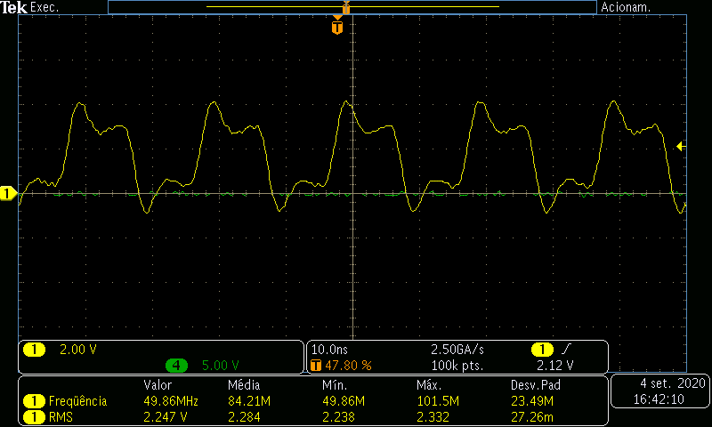
 See below the code I am using for the procedure B. Also, I have attached the memory browser behavior to the code running at EMIF1 at 50MHz (working fine) and at 100MHz (with mirrored data).

// ------------------------------------------------------------------------
// Includes
// ------------------------------------------------------------------------
#include "F2837xD_device.h"
#include "F2837xD_Examples.h"
#include "GPIO.h"
#include "EMIF1.h"

// Defines
//
#define TEST_PASS             0xABCDABCD
#define TEST_FAIL             0xDEADDEAD
#define SDRAM_CS0_START_ADDR  0x80000000
#define SDRAM_CS0_SIZE        0x00800000

//
// Globals
//
Uint16  ErrCount = 0;
Uint32  TEST_STATUS;
Uint32 ii;


void Emif1Config(void)
{
    char ErrCount_local;
    TEST_STATUS = TEST_FAIL;


    EALLOW;
    //
    // Grab EMIF1 For CPU1
    //
    Emif1ConfigRegs.EMIF1MSEL.all = 0x93A5CE71;
    if(Emif1ConfigRegs.EMIF1MSEL.all != 0x1)
    {
       ErrCount++;
    }

    //
    //Disable Access Protection (CPU_FETCH/CPU_WR/DMA_WR)
    //
    Emif1ConfigRegs.EMIF1ACCPROT0.all = 0x0;
    if(Emif1ConfigRegs.EMIF1ACCPROT0.all != 0x0)
    {
       ErrCount++;
    }

    //
    // Commit the configuration related to protection. Till this bit remains
    // set content of EMIF1ACCPROT0 register can't be changed.
    //
    Emif1ConfigRegs.EMIF1COMMIT.all = 0x1;
    if(Emif1ConfigRegs.EMIF1COMMIT.all != 0x1)
    {
       ErrCount++;
    }

    //
    // Lock the configuration so that EMIF1COMMIT register can't be changed
    // any more.
    //
    Emif1ConfigRegs.EMIF1LOCK.all = 0x1;
    if(Emif1ConfigRegs.EMIF1LOCK.all != 1)
    {
       ErrCount++;
    }

    EDIS;

    InitEsaTrdEmif1Gpio();

// Put memory in self refresh mode to change frequency Emif1Regs.SDRAM_CR.bit.SR = 0x1; //Configure to run EMIF1 on half Rate (EMIF1CLK = CPU1SYSCLK/2) // EALLOW; ClkCfgRegs.PERCLKDIVSEL.bit.EMIF1CLKDIV = 0x1; EDIS;

// Release self refresh mode Emif1Regs.SDRAM_CR.bit.SR = 0x0; //Configure SDRAM control registers // Need to be programmed based on SDRAM Data-Sheet. //T_RFC = 60ns = 0x6 //T_RP = 18ns = 0x1 //T_RCD = 18ns = 0x1 //T_WR = 12ns = 0x1 //T_RAS = 42ns = 0x4 //T_RC = 60ns = 0x6 //T_RRD = 12ns = 0x1 Emif1Regs.SDRAM_TR.bit.T_RFC = 0x6; Emif1Regs.SDRAM_TR.bit.T_RP = 0x1; Emif1Regs.SDRAM_TR.bit.T_RCD = 0x1; Emif1Regs.SDRAM_TR.bit.T_WR = 0x1; Emif1Regs.SDRAM_TR.bit.T_RAS = 0x4; Emif1Regs.SDRAM_TR.bit.T_RC = 0x6; Emif1Regs.SDRAM_TR.bit.T_RRD = 0x1; //Txsr = 61.5ns = 0x6 Emif1Regs.SDR_EXT_TMNG.bit.T_XS = 0x6; //Tref = 64ms (15.6us*4096) for 4096 ROW, RR = 64m*100M/4096 = 1562.5 (0x61B) //Emif1Regs.SDRAM_RCR.all = 0x61B;
//Procedure 2 configuration Emif1Regs.SDRAM_RCR.bit.REFRESH_RATE = 0x9C5; //PAGESIZE=1 (elements per ROW), IBANK = 2 (4 BANK), CL = 3, NM = 0 (32bit) //Emif1Regs.SDRAM_CR.all = 0x00000720; Emif1Regs.SDRAM_CR.bit.SR = 0x0; Emif1Regs.SDRAM_CR.bit.NM = 0; Emif1Regs.SDRAM_CR.bit.CL = 0x3; Emif1Regs.SDRAM_CR.bit.BIT_11_9_LOCK = 0x1; Emif1Regs.SDRAM_CR.bit.IBANK = 0x2; Emif1Regs.SDRAM_CR.bit.PAGESIGE = 0x3;
//Add delay to satisfy SDRAM power-up constraint DELAY_US(200);
//Config the SDRAM datasheet refresh rate Emif1Regs.SDRAM_RCR.bit.REFRESH_RATE = 0x61B; // //Add some extra delay // for(ii=0;ii<123;ii++) { } // Basic read/write check. ErrCount_local = sdram_read_write(SDRAM_CS0_START_ADDR, SDRAM_CS0_SIZE); ErrCount = ErrCount + ErrCount_local; //run different addr walk checks ErrCount_local = sdram_addr_walk(SDRAM_CS0_START_ADDR, 15); ErrCount = ErrCount + ErrCount_local; //run different data walk checks ErrCount_local = sdram_data_walk(SDRAM_CS0_START_ADDR, SDRAM_CS0_SIZE); ErrCount = ErrCount + ErrCount_local; //run different data size checks ErrCount_local = sdram_data_size(SDRAM_CS0_START_ADDR, 4); ErrCount = ErrCount + ErrCount_local; if (ErrCount == 0x0) { TEST_STATUS = TEST_PASS; } } // // sdram_data_walk - This function performs a walking 0 & 1 For SDRAM RD & WR // char sdram_data_walk(Uint32 start_addr, Uint32 mem_size) { Uint32 XM_p, XMEM_p; unsigned long sdram_rdl; unsigned long sdram_wdl; int i; int k; int m; XM_p = start_addr; for (i=0; i < mem_size; i=i+64) { for (m=0; m < 2; m++) { XMEM_p = XM_p; // //Write loop // sdram_wdl = 0x0001; for (k=0; k < 32; k++) { if(m==0) { __addr32_write_uint32(XMEM_p, sdram_wdl); } else { __addr32_write_uint32(XMEM_p, ~sdram_wdl); } XMEM_p = XMEM_p+2; sdram_wdl = sdram_wdl<<1; } // //Read loop // XMEM_p = XM_p; sdram_wdl = 0x0001; for (k=0; k < 32; k++) { sdram_rdl = __addr32_read_uint32(XMEM_p); if(m==1) { sdram_rdl = ~sdram_rdl; } if(sdram_rdl != sdram_wdl) { return(1); } XMEM_p = XMEM_p+2; sdram_wdl=sdram_wdl<<1; } } XM_p = XMEM_p; } return(0); } // // sdram_addr_walk - This function performs a toggle on each address bit. // In this case memory assumed is 4Mb. // MA = BA[1:0]ROW[11:0]COL[7:0] // char sdram_addr_walk(Uint32 start_addr, Uint32 addr_size) { Uint32 XMEM_p; unsigned long sdram_rdl; unsigned long sdram_wdl; int i; unsigned long xshift; unsigned long xshift2; // //Write loop // xshift = 0x00000001; sdram_wdl = 0x5678abcd; for (i=0; i < addr_size; i++) { xshift2 = ((xshift+1)<<1); XMEM_p = start_addr + xshift2; __addr32_write_uint32(XMEM_p, sdram_wdl); sdram_wdl = sdram_wdl+0x11111111; xshift = xshift<<1; } // //Read loop // xshift = 0x00000001; sdram_wdl = 0x5678abcd; for (i=0; i < addr_size; i++) { xshift2 = ((xshift+1)<<1); XMEM_p= start_addr + xshift2; sdram_rdl = __addr32_read_uint32(XMEM_p); if( sdram_rdl != sdram_wdl) { return(1); } xshift = xshift<<1; sdram_wdl = sdram_wdl + 0x11111111; } return(0); } // // sdram_data_size - This function performs different data type // (HALFWORD/WORD) access. // char sdram_data_size(Uint32 start_addr, Uint32 mem_size) { unsigned short sdram_rds; unsigned long sdram_rdl; unsigned short sdram_wds; unsigned long sdram_wdl; int i; Uint32 XMEM_p; // //Write data short // XMEM_p = start_addr; sdram_wds = 0x0605; for (i=0; i < 2; i++) { __addr32_write_uint16(XMEM_p, sdram_wds); XMEM_p++; sdram_wds += 0x0202; } // //Write data long // sdram_wdl = 0x0C0B0A09; for (i=0; i < 2; i++) { __addr32_write_uint32(XMEM_p, sdram_wdl); XMEM_p = XMEM_p+2; sdram_wdl += 0x04040404; } // //Read data short // XMEM_p = start_addr; sdram_wds=0x0605; for (i=0; i < 6; i++) { sdram_rds = __addr32_read_uint16(XMEM_p); if( sdram_rds != sdram_wds) { return(1); } XMEM_p++; sdram_wds += 0x0202; } // //Read data long // XMEM_p = start_addr; sdram_wdl=0x08070605; for (i=0; i < 3; i++) { sdram_rdl = __addr32_read_uint32(XMEM_p); if( sdram_rdl != sdram_wdl) { return(1); } XMEM_p = XMEM_p+2; sdram_wdl += 0x04040404; } return(0); } // // sdram_read_write - This function performs simple read/write accesses // to memory. // char sdram_read_write(Uint32 start_addr, Uint32 mem_size) { unsigned long mem_rdl; unsigned long mem_wdl; Uint32 XMEM_p; Uint32 i; // //Write data // XMEM_p = start_addr; // //Fill memory // mem_wdl = 0x01234567; for (i=0; i < mem_size; i++) { __addr32_write_uint32(XMEM_p, mem_wdl); XMEM_p = XMEM_p+2; mem_wdl += 0x11111111; } // //Verify memory // mem_wdl = 0x01234567; XMEM_p = start_addr; for (i=0; i < mem_size; i++) { mem_rdl = __addr32_read_uint32(XMEM_p); if( mem_rdl != mem_wdl) { return(1); } XMEM_p = XMEM_p+2; mem_wdl += 0x11111111; } return(0); }

  • Henrique,

    You can use this configuration tool to check your EMIF settings: ~\C2000Ware_XXXX\boards\TIDesigns\F28379D_EMIF_DC\C2000-EMIF_ConfigurationTool.xlsx

    This appnote has some recommendations for usage and debugging.  And it has additional related examples here: ~\C2000Ware_XXXX\device_support\f2837xd\examples\cpu1\emif_dc_*

    -Tommy

  • Tommy,

    I have already used the spreadsheet to verify all registers configurations. They all seems correct.

    Also, have read the appnote.  you suggested. Can't see any problem with de code and interface.

    Can you please take a closer look at the code?

    Does the EMIF can really operate as 100MHz?

    Henrique.

  • Henrique Chaves said:
    I have already used the spreadsheet to verify all registers configurations. They all seems correct.

    Also, have read the appnote.  you suggested. Can't see any problem with de code and interface.

    Have you tried to slow down the SDRAM timing parameters while still running at 100MHz?  There might only be a timing sensitivity to one or two parameters.

    Henrique Chaves said:
    Can you please take a closer look at the code?

    Since you are able to operate at 50MHz, and you can observe the problem using the memory browser, the code outside of the EMIF configuration is likely not very relevant. What happens if you manually change the contents of a memory location using the memory browser?

    Henrique Chaves said:
    Does the EMIF can really operate as 100MHz?

    Yes. Have you confirmed that SYSCLK is really running at 200MHz by observing XCLKOUT or the EMIF clock?

  • a) Have you tried to slow down the SDRAM timing parameters while still running at 100MHz?  There might only be a timing sensitivity to one or two parameters.

    Yes, I have tryed to increase all timing registers (but not the REFRESH_RATE as mentioned in the appnote) to the maximum value, but still see the same response. Below is what i changed to perform this test:

        Emif1Regs.SDRAM_TR.bit.T_RFC = 0xF;
        Emif1Regs.SDRAM_TR.bit.T_RP = 0x7;
        Emif1Regs.SDRAM_TR.bit.T_RCD = 0x7;
        Emif1Regs.SDRAM_TR.bit.T_WR = 0x7;
        Emif1Regs.SDRAM_TR.bit.T_RAS = 0xF;
        Emif1Regs.SDRAM_TR.bit.T_RC = 0xF;
        Emif1Regs.SDRAM_TR.bit.T_RRD = 0x7;
    
        Emif1Regs.SDR_EXT_TMNG.bit.T_XS = 0x1F;

    b) Since you are able to operate at 50MHz, and you can observe the problem using the memory browser, the code outside of the EMIF configuration is likely not very relevant. What happens if you manually change the contents of a memory location using the memory browser?

    What happens when I manually change the content of a memory location using the memory browser is that the data I changed is mirrored to all memory locations (same behavieor of the second print I sent earlier).

    c) Yes. Have you confirmed that SYSCLK is really running at 200MHz by observing XCLKOUT or the EMIF clock?

    Yes, I can confirm that using PWM outputs and also I have verified the EMIF clock. Please, take a look at it operating at 50MHz and at 100MHz.

    What esle can be done in order to debug this operation?

  • Henrique,

    The SDRAM clock should ideally be a square wave.  For the 100MHz scope shot, it looks sinusoidal.  Can you check to see if the scope is applying a low-pass filter on the channel, or perhaps verify its operation by looking at a clean signal source?  It will be difficult for the SDRAM to interpret its instructions if the signals are not better defined.

    Is this probed near the F28379 pin or the SDRAM pin?  The signal at the SDRAM would be the more critical.  It would also be a good idea to check a few other signals and how well they align with the SDRAM clock.

    -Tommy

  • Tommy,

    The wave seems sinusoidal because my scope bandwidth is limited to 100MHz. I have double checked this measuring the same signal in the 28379D Controlcard.  the measurement is near the SDRAM. They are separated for about 3 cm. The longest trace is about 5 cm.

    What other singnals do you need? I am setting up measurements for the SDKE, CS0, RAS, CAS and WE.

    Henrique.

  • Henrique,

    For the signals, I would defer to your SDRAM datasheet for the command truth table and waveforms:

    -Tommy

  • Hello Tommy,

    I am helping Henrique with this issue and we realized that the writing process to the SDRAM even in 100MHz is working well. We do a lot of writings using 100MHz and then read all in 50MHz, the data are there with no error. If we use 100MHz to see or to confirm the data written, the result is a mirrored situation for all possible positions from 0x8000000 to 0x8FFFFFFF in 28379D (yes, even in out of memory range mapped 0x8000000 to 0x80800000 - 8Mbx32bits) with the last written value. The problem seems concerned just to the reading part showed in that picture with mirrored data in all positions.

    Some idea what memory pin we can observe or where to change parameters to also have the right reading process to the memory?

    In our algorithm used for testing memory, showed before, we do writings and readings, compare the datas, etcetera to have an OK for further use of this peripheral in this frequency desired (100MHz).

    We have two hardware setups identical working in different workspaces, but the behavior above is the same for both. Custom boards with 28379D and SDRAM near as possible to the processor in the same PCB... we checked again the routed tracks and we are discarding layout problems in this moment.

    We will do the same tests with memories from other manufacturer and with other cristal oscillator base frequency. For the tests with above results, we are using an external 10Mhz oscillator for DSP... we are acquiring 20MHz and 25Mhz oscillators to multiply internally by a lower number.

    We are supposing in this moment, besides some bad parameter used, some peculiar effect when multiplying PLL frequency or memory internal structured readings... it sounds possible or acceptable for you? Have you seen it before?

    Do you have an real example using 28379D and SDRAM working well in 100Mhz in EMIF bus? If yes, what partnumber memory is used?

    Thanks

    Taylor

  • ...when I asked for some SDRAM operating in real project that you know, I am talking about memory in 32bits arrangement.

    We found some SDRAM development kit from Texas using 16bits structure I guess, and if I am not wrong, the examples are for 60Mhz in EMIF bus used in an 120Mhz processor.

    In this clock rate, our custom board operate with no error for writing and reading. Actually, the limit for right operation configured is 63,75Mhz in EMIF1 bus (28379D in 125Mhz, very far from our 200Mhz necessity). If the clock rate is increased over than 63,75Mhz in EMIF, the readings in memory browser or in variables from it start to become more and more instable or wrong until achieve that pattern showed before where the EMIF1 frequency is operating in 100Mhz.

    Regards

    Taylor

  • Taylor Wisbeck said:
    I am helping Henrique with this issue and we realized that the writing process to the SDRAM even in 100MHz is working well. We do a lot of writings using 100MHz and then read all in 50MHz, the data are there with no error.

    This is a good observation because you can reduce your focus to the differences between write and read operations.  It looks like most of the command truth table is the same between the two except for WE.  And of course, the DATA + DQM signals are now driven by the SDRAM instead of EMIF.  So I would recommend observing the differing signals on a scope while reading at 50MHz and comparing them to reading at 100MHz to see if there is a difference in signal integrity.

    Taylor Wisbeck said:
    We are supposing in this moment, besides some bad parameter used, some peculiar effect when multiplying PLL frequency or memory internal structured readings... it sounds possible or acceptable for you? Have you seen it before?

    You can use the EMIF CLK signal as a representation of the internal clock as seen by the EMIF module.  If the clock looks clean on the pin, it is most likely fine internally.

    Taylor Wisbeck said:
    Do you have an real example using 28379D and SDRAM working well in 100Mhz in EMIF bus? If yes, what partnumber memory is used?

    Yes, I had pointed Henrique to the EMIF configuration tool, which is located in the same directory as a reference design that runs at 100MHz, and I also pointed to the examples that run on that reference design:

    You can use this configuration tool to check your EMIF settings: ~\C2000Ware_XXXX\boards\TIDesigns\F28379D_EMIF_DC\C2000-EMIF_ConfigurationTool.xlsx

    This appnote has some recommendations for usage and debugging.  And it has additional related examples here: ~\C2000Ware_XXXX\device_support\f2837xd\examples\cpu1\emif_dc_*

    The part numbers used were AS4C16M16SA and IS42S16160J.  These are 16-bit SDRAMs, but the difference with 32-bit SDRAMs is negligible to the EMIF as long as it is configured correctly.

    There are throughput benchmarks in the appnote too.

  • Tommy,

    Thanks for replying. Henrique tried yesterday another memory test algorithm with GPIO config section inside. It works well in 100MHz EMIF bus for writings and READINGS. After that, I put the same GPIO config in our first memory test algorithm and it finally works well. So we concluded that just some bad GPIO EMIF configuration is assigned in the first used algorithm supplied by C2000ware. We will find the difference in settings EMIF GPIOs to confirm and understand the behavior exposed before... maybe some missing/bad internal pullup or overwriting mux configuration or something like that can cause this intable sympton related to clock rate... now just for clarifying.

    Thanks for your supporting.

    Regards.

  • Hi,

    Apparently  I was missing the qualification period configuration to async in all data pins.

    That resolved the problems. I still don't understand why it was operating fine in the 50 MHz configuration, though.

  • Henrique,

    Glad you have it working now. The qualification stage has the potential to insert digital delay when latching of the external signals, depending on how well the GPIO setup time is met by the external signals. At 50-MHz the setup timings are easier to be met so the delay is not as likely to take place.

    -Tommy