This thread has been locked.

If you have a related question, please click the "Ask a related question" button in the top right corner. The newly created question will be automatically linked to this question.

LAUNCHXL-F28379D: ADC with Spi

Part Number: LAUNCHXL-F28379D

hi 

i am using LAUNCHXL-F28379D and program it through simulink .

i am taking signals through the ADC and compute the magnitude then send it through spi ,

the problem is when i enable spi blocking mode the ADC conversion (the sine signal) become digital and not working fine but the spi data is correct

when i disable it the conversion ADC convention work fine (pure sine )   but the other board does not receive the magnitude correctly  (spi data) 

  • Hi Mohamed,

    How fast are you sampling with the ADC?  How often are you taking ADC ISRs and how long do they take?  Are there separate SPI ISRs?  If there are separate SPI ISRs, how long do the SPI ISRs take?

  • Hi Mohamed,

    I would suggest you raise this question on the Mathworks support forum at http://www.mathworks.com/support/.  You can also look through some FAQs on the post below.

  • I am using 7 channel of the adc with sampling rate 0.001 and i didn't configure any ISRS idont know how to configure that in simulink  

  • here the scope of the ADC without the blocking mode but the Data of spi is not correct it varying with latency

  • and here you see in the blocking mode the spi sending correct value but the ADC reading wrong value 

  • Hi Mohamed,

    It seems like the SPI code you are enabling is somehow slowing down the ADC sampling.  Since this is specific to the way that Simulink is structured and synthesizes the code, you should definitely try to get some guidance from the Mathworks support forum as Gus has suggested.     

  • I did but the problem is that sometimes they  take years to answer and its kind of urgent issue for me

  • Hi Mohamed,

    Like I said, my best guess is that while the SPI code is running it is preventing the ADC code from reading the results.  Is there a non-blocking (presumably ISR based) SPI block/module/option?  If possible, you'd also want to use the SPI FIFO to further reduce the CPU overhead. 

    You might also want to investigate the ADC code options to determine if there are options for generating that ADC code that might help with code interaction.


  • here the code generated by simulink for the ADC

    //########################################################################### // FILE: F2837xD_Adc.c // TITLE: F2837xD Adc Support Functions. //########################################################################### // $TI Release: F2837xD Support Library v190 $ // $Release Date: Mon Feb 1 16:51:57 CST 2016 $ // $Copyright: Copyright (C) 2013-2016 Texas Instruments Incorporated - // http://www.ti.com/ ALL RIGHTS RESERVED $ //########################################################################### #include "F2837xD_device.h" // F2837xD Headerfile Include File #include "F2837xD_Examples.h" // F2837xD Examples Include File /* * Set the resolution and signalmode for a given ADC. This will ensure that * the correct trim is loaded. */ void AdcSetMode(Uint16 adc, Uint16 resolution, Uint16 signalmode) { Uint16 adcOffsetTrimOTPIndex; //index into OTP table of ADC offset trims Uint16 adcOffsetTrim; //temporary ADC offset trim //re-populate INL trim CalAdcINL(adc); if(0xFFFF != *((Uint16*)GetAdcOffsetTrimOTP)){ //offset trim function is programmed into OTP, so call it //calculate the index into OTP table of offset trims and call //function to return the correct offset trim adcOffsetTrimOTPIndex = 4*adc + 2*resolution + 1*signalmode; adcOffsetTrim = (*GetAdcOffsetTrimOTP)(adcOffsetTrimOTPIndex); } else { //offset trim function is not populated, so set offset trim to 0 adcOffsetTrim = 0; } //Apply the resolution and signalmode to the specified ADC. //Also apply the offset trim and, if needed, linearity trim correction. switch(adc){ case ADC_ADCA: AdcaRegs.ADCCTL2.bit.RESOLUTION = resolution; AdcaRegs.ADCCTL2.bit.SIGNALMODE = signalmode; AdcaRegs.ADCOFFTRIM.all = adcOffsetTrim; if(ADC_RESOLUTION_12BIT == resolution){ //12-bit linearity trim workaround AdcaRegs.ADCINLTRIM1 &= 0xFFFF0000; AdcaRegs.ADCINLTRIM2 &= 0xFFFF0000; AdcaRegs.ADCINLTRIM4 &= 0xFFFF0000; AdcaRegs.ADCINLTRIM5 &= 0xFFFF0000; } break; case ADC_ADCB: AdcbRegs.ADCCTL2.bit.RESOLUTION = resolution; AdcbRegs.ADCCTL2.bit.SIGNALMODE = signalmode; AdcbRegs.ADCOFFTRIM.all = adcOffsetTrim; if(ADC_RESOLUTION_12BIT == resolution){ //12-bit linearity trim workaround AdcbRegs.ADCINLTRIM1 &= 0xFFFF0000; AdcbRegs.ADCINLTRIM2 &= 0xFFFF0000; AdcbRegs.ADCINLTRIM4 &= 0xFFFF0000; AdcbRegs.ADCINLTRIM5 &= 0xFFFF0000; } break; case ADC_ADCC: AdccRegs.ADCCTL2.bit.RESOLUTION = resolution; AdccRegs.ADCCTL2.bit.SIGNALMODE = signalmode; AdccRegs.ADCOFFTRIM.all = adcOffsetTrim; if(ADC_RESOLUTION_12BIT == resolution){ //12-bit linearity trim workaround AdccRegs.ADCINLTRIM1 &= 0xFFFF0000; AdccRegs.ADCINLTRIM2 &= 0xFFFF0000; AdccRegs.ADCINLTRIM4 &= 0xFFFF0000; AdccRegs.ADCINLTRIM5 &= 0xFFFF0000; } break; case ADC_ADCD: AdcdRegs.ADCCTL2.bit.RESOLUTION = resolution; AdcdRegs.ADCCTL2.bit.SIGNALMODE = signalmode; AdcdRegs.ADCOFFTRIM.all = adcOffsetTrim; if(ADC_RESOLUTION_12BIT == resolution){ //12-bit linearity trim workaround AdcdRegs.ADCINLTRIM1 &= 0xFFFF0000; AdcdRegs.ADCINLTRIM2 &= 0xFFFF0000; AdcdRegs.ADCINLTRIM4 &= 0xFFFF0000; AdcdRegs.ADCINLTRIM5 &= 0xFFFF0000; } break; } } /* * Loads INL trim values from OTP into the trim registers of the specified ADC. * Use only as part of AdcSetMode function, since linearity trim correction * is needed for some modes. */ void CalAdcINL(Uint16 adc) { switch(adc){ case ADC_ADCA: if(0xFFFF != *((Uint16*)CalAdcaINL)){ //trim function is programmed into OTP, so call it (*CalAdcaINL)(); } else { //do nothing, no INL trim function populated } break; case ADC_ADCB: if(0xFFFF != *((Uint16*)CalAdcbINL)){ //trim function is programmed into OTP, so call it (*CalAdcbINL)(); } else { //do nothing, no INL trim function populated } break; case ADC_ADCC: if(0xFFFF != *((Uint16*)CalAdccINL)){ //trim function is programmed into OTP, so call it (*CalAdccINL)(); } else { //do nothing, no INL trim function populated } break; case ADC_ADCD: if(0xFFFF != *((Uint16*)CalAdcdINL)){ //trim function is programmed into OTP, so call it (*CalAdcdINL)(); } else { //do nothing, no INL trim function populated } break; } }

  • and here the code for spi generated by simulink i have zero experience with ccs so icant understand it or which file there you want me to open 


    /* Copyright 2017-18 The MathWorks, Inc. */ #include "MW_c28xSPI.h" #include "MW_SPI.h" /* Intialize SPI device */ MW_Handle_Type MW_SPI_Open(uint32_T SPIModule, uint32_T MosiPin, uint32_T MisoPin, uint32_T ClockPin, uint32_T SlaveSelectPin, uint8_T ActiveLowSSPin, uint8_T spi_device_type) { #ifndef MATLAB_MEX_FILE MW_SpiHandle mySpi; mySpi = SPI_init(SPIModule); #ifndef MW_F281X if(SlaveSelectPin != MW_UNDEFINED_VALUE) { Set_GPIOPin(SlaveSelectPin, GPIO_MUX_CPU1, 0, GPIO_OUTPUT, GPIO_PULLUP|GPIO_ASYNC); } #endif return (MW_Handle_Type)mySpi; #else return (MW_Handle_Type)NULL; #endif //MATLAB_MEX_FILE } /* Set SPI Communication format for the processor */ /* targetprecision: Bits/frame for processor */ /* spi_mode: Clock polarity and clock phase */ /* TargetFirstBitToTransfer: First bit to be transferred by processor */ MW_SPI_Status_Type MW_SPI_SetFormat(MW_Handle_Type SPIModuleHandle, uint8_T targetprecision, MW_SPI_Mode_type spi_mode, MW_SPI_FirstBitTransfer_Type TargetFirstBitToTransfer) { #ifndef MATLAB_MEX_FILE MW_SpiHandle mySpi = (MW_SpiHandle)SPIModuleHandle; if((mySpi->spi_clk_mode == (Uint16)spi_mode) && (mySpi->charLength == targetprecision)) { // Do nothing when there is no change in the parameters return MW_SPI_SUCCESS; } else { volatile struct SPI_REGS *SPI = (struct SPI_REGS *)mySpi->spi_base_address; // Update the SPI clock mode and Charecter length mySpi->charLength = targetprecision; mySpi->spi_clk_mode = (Uint16)spi_mode; (*SPI).SPICCR.bit.SPISWRESET = 0; if (mySpi->spi_clk_mode == MW_SPI_MODE_0) { (*SPI).SPICCR.bit.CLKPOLARITY = 0; (*SPI).SPICTL.bit.CLK_PHASE = 0; } else if (mySpi->spi_clk_mode == MW_SPI_MODE_1) { (*SPI).SPICCR.bit.CLKPOLARITY = 0; (*SPI).SPICTL.bit.CLK_PHASE = 1; } else if (mySpi->spi_clk_mode == MW_SPI_MODE_2) { (*SPI).SPICCR.bit.CLKPOLARITY = 1; (*SPI).SPICTL.bit.CLK_PHASE = 0; } else { (*SPI).SPICCR.bit.CLKPOLARITY = 1; (*SPI).SPICTL.bit.CLK_PHASE = 1; } (*SPI).SPICCR.bit.SPICHAR = (uint16_T)((mySpi->charLength) - 1); (*SPI).SPICCR.bit.SPISWRESET = 1; return MW_SPI_SUCCESS; } #else return MW_SPI_SUCCESS; #endif //MATLAB_MEX_FILE } /* Set SPI bus speed */ MW_SPI_Status_Type MW_SPI_SetBusSpeed(MW_Handle_Type SPIModuleHandle, uint32_T BusSpeedInHz) { #ifndef MATLAB_MEX_FILE return MW_SPI_SUCCESS; #else return MW_SPI_SUCCESS; #endif //MATLAB_MEX_FILE } /* Configure SPI Slave select pin before starting the transmission if the slave select Pin is not custom */ MW_SPI_Status_Type MW_SPI_SetSlaveSelect(MW_Handle_Type SPIModuleHandle, uint32_T SlaveSelectPin, uint8_T ActiveLowSSPin) { #ifndef MATLAB_MEX_FILE return MW_SPI_SUCCESS; #else return MW_SPI_SUCCESS; #endif //MATLAB_MEX_FILE } /* Initiate combined SPI transmission from master to slave */ MW_SPI_Status_Type MW_SPI_MasterWriteRead_8bits(MW_Handle_Type SPIModuleHandle, const uint8_T * wrData, uint8_T * rdData, uint32_T datalength) { #ifndef MATLAB_MEX_FILE MW_SpiHandle mySpi = (MW_SpiHandle)SPIModuleHandle; volatile struct SPI_REGS *SPI = (struct SPI_REGS *)mySpi->spi_base_address; uint32_T localVar; uint16_T *readdata = (uint16_T*) rdData; uint16_T *writedata = (uint16_T*) wrData; for (localVar = 0; localVar < datalength; localVar++) { while ((*SPI).SPIFFTX.bit.TXFFST == mySpi->fifoLevel) { /*Wait until Tx buffer is cleared*/ } (*SPI).SPITXBUF = writedata[localVar] << (16 - mySpi->charLength); while ((*SPI).SPIFFRX.bit.RXFFST == 0) { /*Wait until Rx buffer has data*/ } readdata[localVar] = (*SPI).SPIRXBUF & (((Uint32)1 << mySpi->charLength) - 1); } return MW_SPI_SUCCESS; #else return MW_SPI_SUCCESS; #endif //MATLAB_MEX_FILE } /* Initiate data communication from master to slave in slave mode */ MW_SPI_Status_Type MW_SPI_SlaveWriteRead_8bits(MW_Handle_Type SPIModuleHandle, const uint8_T * wrData, uint8_T * rdData, uint32_T datalength) { #ifndef MATLAB_MEX_FILE return MW_SPI_SUCCESS; #else return MW_SPI_SUCCESS; #endif //MATLAB_MEX_FILE } /* Get the status of SPI */ MW_SPI_Status_Type MW_SPI_GetStatus(MW_Handle_Type SPIModuleHandle) { #ifndef MATLAB_MEX_FILE return MW_SPI_SUCCESS; #else return MW_SPI_SUCCESS; #endif //MATLAB_MEX_FILE } /* De-initialize or release the SPI */ void MW_SPI_Close(MW_Handle_Type SPIModuleHandle, uint32_T MosiPin, uint32_T MisoPin, uint32_T ClockPin, uint32_T SlaveSelectPin) { }

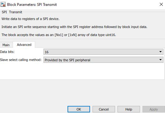
  • and here the spi configuration from simulink

  • Mohamed,

    As Devin has mentioned, and I think you understood when you observed this issue was some contention of system resources when SPI is placed in blocking mode(I'm assuming blocking here, means highest priority ISR)

    One or both of the two things is likely the cause

    1)SPI blocking is interfering with the ADC start of conversion frequency.  This would only be true if you are manually triggering the ADC by setting the SOC Force bit in SW.  Can you comment on the trigger source for the ADC channel, i.e. PWM, Timer, or SW?

    2)SPI block is interfering with reading the ADC results in time, before they are overwritten.  To remedy this, I'd like to try and use the DMA to read the ADC results vs the CPU.  Is there an obvious block for the DMA in Simulink?  If so we should point the read function to the ADC result regs, and the destination to a block of RAM big enough to hold your data.

    Let me know if you think #1 or #2 is more likely and if we need help from MW to implement.

    Best,

    Matthew

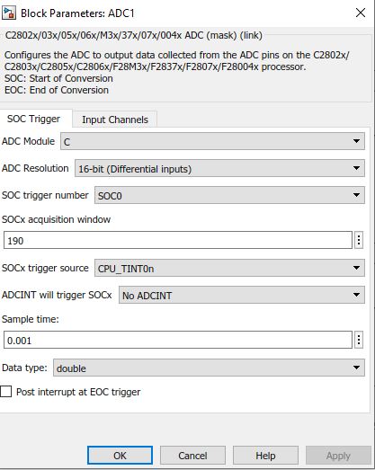
  • here the ADC triggering source which is cpu timer 0

  • and fro DMA 

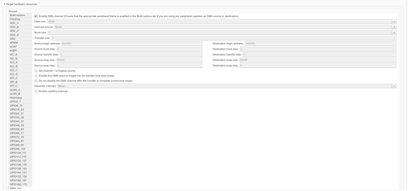
    here what we have in simulink the first the option of DMA in the first pic if i enable it is the same i don't now if i have to configure something else and the second Pic its DMA ch1 configuration but i don't know how to configure it   

  • Mohamed,

    I'll look into the DMA a bit more, is it possible that the SPI is using the same CPU Timer0 resource to initiate its conversions?

    Best,

    Matthew

  • That what i thought in the beginning so i changed the ADC to CPU time 2 but i got the same result 

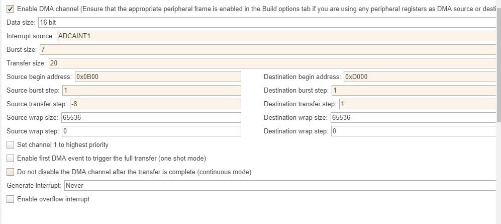
  • I've attached a screenshot of the DMA setup below; there are likely a few things we need to change to match your setup:

    I believe you are using ADCA, you just need to make sure you are picking the same INT source as you had before for your ISR(you'll want to remove any copy code you had in the ISR itself since the DMA will take care of that).

    For the Burst Size, this is how many ADC samples are taken when it receives its Start of Conversion -1, So in the below case I have assumed there are 8 samples for every SOC.  Please change this accordingly.

    Transfer Size is the length of your data buffer divided by the burst size -1.

    The source begin address is the ADC Result registers 0xB00, and the dest addr is whatever RAM you were storing the results in.

    Burst step is the increment for each burst word, in this case if your sampling the same channel 8 times, we just want to increment through the ADC Result one at a time.  Same for the destination burst step

    Transfer Step is what we want to happen to the source/dest address on each new transfer, in this case for the source we need to make it -8 to start at the beginning of the ADC Result Register each time.  For the dest, we want to place this new data right after the old data, so we just put a "1"

    I've unchecked continuous mode for the sake of debug here, i.e. the DMA will stop once the buffer is full.  You could configure this to on, but the data will be overwritten in your buffer the next ADC SOC.

  • thank you for you response to give you the full picture i am using 7 ADC three for the voltage two for the current which are 3 from ADCA ,Two from ADCC and two From ADCB so what do you recommend in this case i use 3 DMA channels for A and B and C and do i have to change the address ? 

    my sampling rate is 0.001s 

  • I Can send you my simulink file if you want to see all the component that i am using.

  • Mohamed,

    Please go ahead and send me the file; I can try to change the DMA settings accordingly.

    Best,

    Matthew

  • this is the simulink file if you are using matlab 2018b or higher version it will work for you but if you are using lower version please inform me which version you are using and i will export the simulink file to it , thank you

    c2000final2.rar

  • Mohamed,

    Thanks, I'm able to open and view the simulink model.  I'm going to need a few days to ping the MW team on the best way to proceed.  I believe that the MW ADC blocks are polling the ADC EOC bits individually(this is not incorrect BTW just pointing this out); so this would agree with our hypothesis on the resource crunch.  There may be an easier way to proceed vs the DMA.

    Best,

    Matthew

  • ok, thank you i will be waiting for your response. 

  • Mohamed,

    I spoke with the MW team, and they offered to help here.  Would it be possible to file a post on their forum or open a support ticket and reference this post(they are aware)? 

    You can let me know if you have any issue doing that, but I think there is a level of abstraction they can help clear up more quickly than we can inside TI.

    I'm going to leave the thread open, however, please reply back if you have any issues.

    Best,
    Matthew

  • i did last month but no one answered me.

    you can see at the link below

    www.mathworks.com/.../601387-adc-with-spi-launchxl-f28379d-simulink

  • I'll let the MW team know, appreciate the heads up on this.

    Best,
    Matthew

  • i don't think they will help me , i did what the request but the also requested the licence number of the product , and the thing is i am using my university lab for this project which i don't have access to it at the moment due to covid-19 restriction , what i was planning to do is to get the solution then i request from my professor to grant me an access for one day because it long process and a lot of people need to approve me entering the university during the  pandemic, i wote them my explanation and i didnt get response from them yet , i hope they understand the situation. 

  • Mohamed,

    I understand, I'll check back with them on the topic you mention.

    Best,

    Matthew

  • this is what they send  me today and i don't have this.

    Please send the following information:

    1) The complete output displayed after entering the following command:>> ver -supportThis command should be entered at the MATLAB command line. The output will provide us with details regarding your license, product, and platform.

    Access to our technical support team is one of the benefits of maintaining an active Software Maintenance Service (SMS) subscription with your license. We look forward to getting this information from you so that we may assist you with your technical issue.

  • Hi Mohamed,

    Sorry for your difficulties.

    MathWorks Tech Support needs this information so they can log your case, and search our vast database of existing solutions for the help you need. Without it, we cant assist you properly.

    I would advise looking at trying to set up a remote login or remote desktop and using that to access MATLAB and get the license # and version info. You can also probably get our Mobile app (available on iPhone and Android stores) to connect to your / license session at your University, and work from there to get the info you require. 

    Cheers,

    -Brian

  • That will be a little bit hard because most of the faculty is working from home due to the pandemic and granting premonition  to use the lab is pretty hard

  • i provided them with my licence but they responded that my license is out of maintenance. and they require me to take some subscription so they will not support me until i do the subscription which is not free, so any suggestion or idea from texas team on  how can i solve the issue and what to change the simulink file ?      

  • Mohamed,

    I understand the situation.  I'm going to get something more concrete by Tues of next week; but after talking with the MW team I think I understand what the issue may be.  The ADC blocks not only initialize the ADC modules, but they use the CPU to do a periodic read of those result registers(and I think CPU1 Timer is involved as well).  I think that when we block for SPI we are consuming the CPU MIPs necessary to read the output either at all or on time.

    I think there are a few ways around this, I would not use the output of those blocks to read the ADC values, rather I would use the DMA to read the ADC results once they are updated.  We should be able to do this by feeding a ADC interrupt to the DMA block; and then have the DMA copy all/some of the registers to memory.  Once that has completed we can use the DMA to send its interrupt/done signal to the C28x and then read the results that way.

    I will try and get some example Simulink blocks by next week, but if you can find the DMA block you can try to set it up yourself.  I'd recommend taking a look at the DMA chapter in the TRM 

    Best,

    Matthew

  • Sure I will read the chapter,  the thing is the documantation from math work is not that clear and I didn't find an example in how to use it if could understand it from them that will be great .

    Thank you for you valuable time .