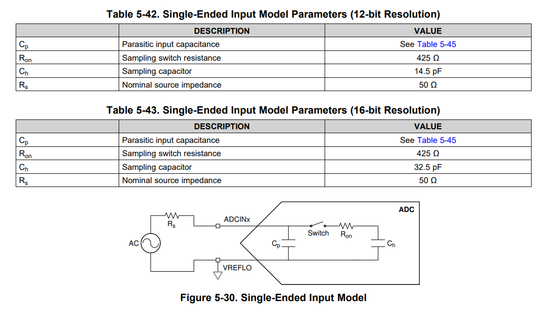
This thread has been locked.

If you have a related question, please click the "Ask a related question" button in the top right corner. The newly created question will be automatically linked to this question.

TMS320F28388D: ADC Reading noise when not grounded

Part Number: TMS320F28388D


Hi,

I am checking the ADC values using the example program to read Channel A2, A3, and B2, B3 using the Software Trigger.

The data I see seems to be irrelevant. 

When I give input to one channel, I see some percentage of data being displayed on other channels.

When I ground the immediate channel, the extra data gets back to zero on the neighbor channels.

The snapshot is for the input of 2.5V for A2 and A3 floating

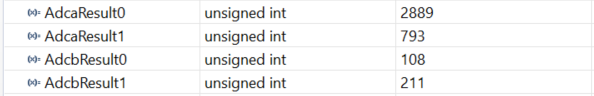
The below snapshot is for the input of 2.5v and A3 connected to ground

I expected all to be zero or very minimal when nothing is fed. I am using TI control card for this experiment.

regards,

Mohan

  • Hi Mohan,

    You should not expect floating channels to read near ground, but instead for the results to be undefined. 

    The floating channels producing a reading based on the previously sampled channel is expected, but you should not depend on this property. 

  • Hi Devin,

    Thank you for your response, however, I was not expecting a near-zero value for it.

    If you observe in the snapshot, for Adca result register the count is 793 for a not connected scenario. 

    If you notice, it's 20% of the final value for the ADC. Is 20% fluctuation expected when not connected?

    I could not understand the statement that  " reading based on the previously sampled channel is expected, but you should not depend on this property. "

    one channel should not overlap with other right?

  • Hi Mohan,

    You should treat the results of undriven ADC channels as undefined.  20% fluctuation is therefore acceptable, as would any conversion results between 0 and 4095 in any sequence (in 12-bit mode).    

    When driving the ADC in normal operation, it is necessary to make sure the capacitance (Ch) of the S+H circuit is adequately charged to within 1/2 LSBs (or another acceptable level or error tolerance) of the applied source voltage.  This needs to consider the internal ADC model (usually Ch and a switch resistance, Ron) as well as the impedance of the external driver (usually at least an external C, Cs, and an external resistance, Rs).  In the worst-case analysis, it is best to assume that Ch starts from 0V and is being driven to VREFHI or Ch starts at VREFHI and is being driven to 0V. 

    However, depending on the specific ADC implementation, Ch will usually start at a voltage near the previous conversion instead of at 0V or VREFHI because the ADC is using the same S+H circuit (and thus the same Ch) for sequential conversions.  In the case of a normal ADC channel that is driven by a source, but where the source impedance is too high and/or the S+H duration is too short, Ch doesn't get completely driven to the new voltage and the result is that the previous conversion has some influence on the current conversion, resulting in a "memory cross-talk" error.  When the current channel is undriven, the memory cross-talk effect becomes very pronounced.  Other architectural quirks may also influence the conversion result when the input is completely un-driven, so you shouldn't try to rely on this memory property. 


  • Hi Devin,

    Thank you for such a detailed explanation. 

    I understand better now, and after discussing with the hardware team, I figured out that in my program that they do have a circuit to drive the ADC properly.

    So, it is expected to read the values in the experimenter kit as it might not have the additional circuitry needed for ADC.

    Thank you

    Mohan