This thread has been locked.

If you have a related question, please click the "Ask a related question" button in the top right corner. The newly created question will be automatically linked to this question.

ADC Acquisition window calculation

Part Number: TMS320F280049

Hi Team,

I am trying to configure 280049`s ADC for my project. I have some doubts regarding the ADC acquisition window calculation explained in TRM. The following are my questions,

1. The settling error explained in the section 13.15.2 raises some doubts. It is said that the the sampling capacitor should be charged to 1/4 LSB or 1/2 LSB of final value. The LSB value of  my ADC is around 0.000732V. So in the equation provided in the same section (given below) which value for settling error should I consider while evaluating the equation. If settling error is 1/4 LSB should I use 1/4 LSB or 0.000183 (= 0.000732 / 4) ?

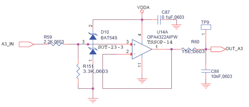
2. How to calculate values Cs and Rs in the following equation for my ADC driving circuit given below ,

I considered Cs as 10 nF and Rs as 15 ohms, is this assumption is correct?

3. Is this ADC is capable of double ended single inputs or single ended only ?

4. Will it cause any problem to simultaneous sampling, if I use different channels with different Cp values leading to different ACQPS value. If that is the case is the EOC generation will be at the end of the conversion of channel with largest SH + acquisition window ?

5. If ADC sampling is controlled by SOC which is in turn generated using ePWM in my application, I wonder what is the importance of ADCCLK in sampling ? Do I need to choose a specific value for ADC clock, according to each circuit. If yes, what will be the criterion for choosing the ADC clock for a specific application?

Best Regards,

Vineeth N 

  • Hi Vineeth,

    (1) Settling error in the first term should be in LSBs (LSBs is the unit of 2^N). Alternately you could use ln(ADC full-scale voltage / settling target in volts) for the first term.

    (2) Yes, in your circuit Cs is 10nF and Rs is 15 ohms. 10nF is pretty high.  Cs is usually set at 20 * Ch, which for this ADC would be more in the ballpark of 200-300pF. 

    (3) Single-ended only for this ADC. F2837xD, F2837xS, and F2838x families support fully differential signaling.  

    Note that there are separate PGA grounds on this device if you are using the PGAs and want to run the signal + ground on parallel lines all the way to the PGA input.   

    (4) If you are sampling SOCs in parallel, you'd use the longest S+H duration for all of them.  Cp is probably not going to relatively make too much difference in this case, except for the channel that has VDAC mux'ed with it.

    (5) The S+H is clocked from SYSCLK, so ADCCLK has no effect on the S+H process.  ADCCLK should more-or-less always be set as close to the maximum (50MHz) as possible without going over, as there are no advantages to clocking it slower.  Generally, the use case where you would worry about re-configuring the ADCCLK would be if you are trying to run the SYSCLK slower (for instance, to save power, although note that reducing the ADCCLK does not save power).   

  • Hi Devin,

    Thank you for your quick response. 

    Devin Cottier said:
    (1) Settling error in the first term should be in LSBs (LSBs is the unit of 2^N). Alternately you could use ln(ADC full-scale voltage / settling target in volts) for the first term.

    Can you please explain this a bit more. I didn`t get the concept of LSBs. I have an ADC with 12 bit resolution, so what will be my LSB ?. Is it 1 or Vref / 2^N ?

    Expect this all other answers are clear and to the point. Thank you once again.

    Best Regards,

    Vineeth N

  • Hi Vineeth,

    A 12-bit ADC will have 2^12 possible output values: 0 to 4095 in this case.  If the full-scale range of the ADC is 0 to 3V, then each state will correspond to a voltage step of 3.0V / 4096 = 732uV.  So in this case, 1 LSB = 732uV. 

    For another ADC that was say 14-bits and had 2.5V range, 1 LSB = 2.5V / 16384 = 153uV

    Many times LSBs are a more appropriate unit of measurement than volts when talking about ADC errors because the errors scale with reference voltage. 

  • Hi Devin,

    Thank you for your reply, it is now clear to me. As already said, the settling error term in the calculation for acquisition window in TRM is little bit confusing, I must say. Because in the section 13.15.2, it is said that "the settling error should be 1/4 LSB or 1/2 LSB of the final value " is raising some confusion. Since LSBs are expressed in volts, the natural tendency is to calculate 1/4*732uV ( = 183uV). And put this 183uV directly in to the equation to evaluate 'k', and obviously the result will be incorrect. As you made it clear now, I understand that I should use 0.25 as LSB (=1*1/4) if I use 2^N as FSR or 183uV  as LSB if I use 3V as FSR. If this sounds to be valid point, please consider it on your future revisions of TRM. 

    Thank you once again for your support, means a lot. 

    Best Regards,

    Vineeth N

  • Hi Vineeth,

    You said: "Since LSBs are expressed in volts". 

    I don't think this is quite correct.  LSBs can be converted to volts if you know the ADC range, but LSBs are an alternate unit.  If you have a settling target in LSBs and you know the ADC full-scale range in LSBs (always 2^N, so 4096 for a 12-bit ADC) you can do all your calculations in LSBs without ever having to convert anything to volts.  

    It makes sense to have your settling target be 1/2 LSBs instead of a specific voltage (say 400uV) because settling to 1/2 LSBs gives you the same error magnitude as the quantization error of the ADC (also 1/2 LSB).  

  • Hi Devin,

    Devin Cottier said:
    It makes sense to have your settling target be 1/2 LSBs instead of a specific voltage (say 400uV) because settling to 1/2 LSBs gives you the same error magnitude as the quantization error of the ADC (also 1/2 LSB).

    I might be misunderstood this point, now it is clear.

    Thank you for your quick responses and strong support.

    Best Regards,

    Vineeth N