Part Number: TMS320F28335
Hello,
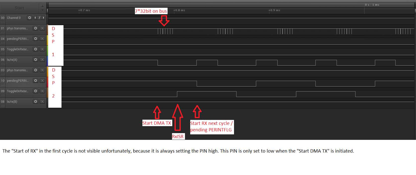
I got sporadic issues with my McBsp (DMA) communication.
This is the general setup:
- Data (7 * 32bit) is transmitted from one C2000 to another C2000 every 62.5µs (16kHz).
- Both C2000 dsps receive as well as transmit the data cyclically.
- The data is checked for consistency each time. (kind of CRC)
- The two boards are synced via optical link (PWMSync)
Problem description:
The received values appear to be shifted sometimes. The values expected at the first 32-Bits seem to be placed where the second 32-Bits should actually be. It seems, that the first 32-Bit value could be from the previous cycle. The timing, however, looks fine with the scope: It seems more like a register setup issue, so I tried to reset the DMA and McBsp registers before starting a new receive every time.
This seems to solve the sporadic issue, however, when I wanted to have proof, if there's really something wrong with one or the other register, I could't find any. The additional debug code could have changed the behavior again, which now would point to a timing issue.
I found the issue in the E2E (https://e2e.ti.com/support/microcontrollers/c2000/f/171/t/348215?tisearch=e2e-sitesearch&keymatch=dma%2525252028335) that F28335 is not able to work with DMA + 32-Bit data. As we are using this in our project I tried if the issue is gone by changing it to 16-bit. ... This didn't solve the issue.
Furthermore, there exists an example: "Example_2823xMcBSP_DLB_DMA.c" which is offering the useage of 32-bit communication. As our communication works except for the sporadic issues at startup, I think this is not the problem.
Can you have a look if the initial settings for the communicaiton are correct. Do you have any idea how to track down such an issue? What needs to be done cyclically before each new transmit/receive?
The initial register settings are the following
//McBSP_init_values
    EALLOW;
    McbspbRegs.SPCR2.all		= 0x0000
    McbspbRegs.SPCR1.all		= 0x0000
    McbspbRegs.SPCR1.bit.DLB 	= 0
    McbspbRegs.MFFINT.all		= 0x0
    McbspbRegs.RCR2.all			= 0x0
    McbspbRegs.RCR1.all			= 0x0
    McbspbRegs.XCR2.all			= 0x0
    McbspbRegs.XCR1.all			= 0x0
    McbspbRegs.SRGR2.bit.CLKSM  = 1
    McbspbRegs.SRGR2.bit.FPER   = 31
    McbspbRegs.SRGR1.bit.FWID   = 0
    McbspbRegs.SRGR1.bit.CLKGDV = 11
    McbspbRegs.PCR.bit.FSXM 	= 1
    McbspbRegs.PCR.bit.CLKXM 	= 1
    McbspbRegs.XCR1.bit.XWDLEN1 = 5
    McbspbRegs.RCR1.bit.RWDLEN1 = 5

    //************* Enable Sample rate generator
    McbspbRegs.SPCR2.bit.GRST = 1; // Enable the sample rate generator
    delay_loop();                 // Wait at least 2 SRG clock cycles
    McbspbRegs.SPCR2.bit.XRST = 1; // Release TX from Reset
    McbspbRegs.SPCR1.bit.RRST = 1; // Release RX from Reset
    McbspbRegs.SPCR2.bit.FRST = 1; // Frame Sync Generator reset
    EDIS;

//DMA_init_values
		//TX-Channel
		DmaRegs.CH1.MODE.bit.PERINTSEL 		= 16
		DmaRegs.CH1.BURST_SIZE.all 			= 1
		DmaRegs.CH1.SRC_BURST_STEP 			= 1
		DmaRegs.CH1.DST_BURST_STEP			= 1
		DmaRegs.CH1.TRANSFER_SIZE 			= 6
		DmaRegs.CH1.SRC_ADDR_SHADOW 		= 0xDFE4
		DmaRegs.CH1.SRC_BEG_ADDR_SHADOW 	= 0xDFE4
		DmaRegs.CH1.DST_ADDR_SHADOW 		= &McbspbRegs.DXR2.all
		DmaRegs.CH1.DST_BEG_ADDR_SHADOW 	= &McbspbRegs.DXR2.all
		DmaRegs.CH1.SRC_WRAP_STEP 			= 0
		DmaRegs.CH1.SRC_WRAP_SIZE 			= 0xFFFF
		DmaRegs.CH1.DST_WRAP_STEP 			= 0
		DmaRegs.CH1.DST_WRAP_SIZE 			= 0xFFFF
		DmaRegs.CH1.SRC_TRANSFER_STEP 		= 1
		DmaRegs.CH1.DST_TRANSFER_STEP 		= 0xFFFF
		DmaRegs.CH1.CONTROL.bit.SYNCCLR 	= 1
		DmaRegs.CH1.CONTROL.bit.ERRCLR		= 1
		DmaRegs.CH1.MODE.bit.SYNCE 			= 0
		DmaRegs.CH1.MODE.bit.SYNCSEL 		= 0
		DmaRegs.CH1.MODE.bit.CHINTE 		= 1
		DmaRegs.CH1.MODE.bit.CHINTMODE 		= 1
		DmaRegs.CH1.MODE.bit.PERINTE 		= 1
		DmaRegs.CH1.CONTROL.bit.PERINTCLR 	= 1
		DmaRegs.CH1.MODE.bit.ONESHOT 		= 0

		//RX-Channel
		DmaRegs.CH2.MODE.bit.PERINTSEL 		= 17
		DmaRegs.CH2.BURST_SIZE.all 			= 1
		DmaRegs.CH2.SRC_BURST_STEP 			= 1
		DmaRegs.CH2.DST_BURST_STEP			= 1
		DmaRegs.CH2.TRANSFER_SIZE 			= 6
		DmaRegs.CH2.SRC_ADDR_SHADOW 		= &McbspbRegs.DRR2.all
		DmaRegs.CH2.SRC_BEG_ADDR_SHADOW 	= &McbspbRegs.DRR2.all
		DmaRegs.CH2.DST_ADDR_SHADOW 		= 0xDFF2
		DmaRegs.CH2.DST_BEG_ADDR_SHADOW 	= 0xDFF2
		DmaRegs.CH2.SRC_WRAP_STEP 			= 0
		DmaRegs.CH2.SRC_WRAP_SIZE 			= 0xFFFF
		DmaRegs.CH2.DST_WRAP_STEP 			= 0
		DmaRegs.CH2.DST_WRAP_SIZE 			= 0xFFFF
		DmaRegs.CH2.SRC_TRANSFER_STEP 		= 0xFFFF
		DmaRegs.CH2.DST_TRANSFER_STEP 		= 1
		DmaRegs.CH2.CONTROL.bit.SYNCCLR 	= 1
		DmaRegs.CH2.CONTROL.bit.ERRCLR		= 1
		DmaRegs.CH2.MODE.bit.SYNCE 			= 0
		DmaRegs.CH2.MODE.bit.SYNCSEL 		= 0
		DmaRegs.CH2.MODE.bit.CHINTE 		= 1
		DmaRegs.CH2.MODE.bit.CHINTMODE 		= 1
		DmaRegs.CH2.MODE.bit.PERINTE 		= 1
		DmaRegs.CH2.CONTROL.bit.PERINTCLR 	= 1
		DmaRegs.CH2.MODE.bit.ONESHOT 		= 0
Cyclically the following is done:
1. DMA-TX-Buffer (0xDFE4) is filled
2. DMA started:
DmaRegs.CH1.CONTROL.bit.RUN = 1
3. DMA-TX-ISR
    EALLOW;
    DmaRegs.CH1.CONTROL.bit.HALT = 1;
    EDIS;
4. DMA-ISR
    EALLOW;
    DmaRegs.CH2.CONTROL.bit.HALT = 1;
    McbspbRegs.SPCR1.bit.RRST = 0;
    EDIS;
5. Make memcopy of data to separate rx-buffer
6. later in loop, copy data from rx-buffer to where it is needed
7. prepare for new receive:
    EALLOW;
    McbspbRegs.SPCR1.bit.RRST = 1;
    EDIS;
    asm(" nop");
    asm(" nop");
    asm(" nop");
    asm(" nop");
    asm(" nop");
    EALLOW;
    DmaRegs.CH2.CONTROL.bit.RUN = 1;
    EDIS;

8. --- repeat ---
Change after which the sporadic issue didn't occur again:
Point 7. (prepare for new receive) from above has been modified:
	EALLOW;
	McbspbRegs.SPCR1.bit.RRST = 0;
	EDIS;

	EALLOW;
	DmaRegs.CH2.CONTROL.bit.SYNCCLR 	= 1;
	DmaRegs.CH2.CONTROL.bit.ERRCLR 		= 1;
	DmaRegs.CH2.CONTROL.bit.PERINTCLR 	= 1;
	DmaRegs.CH2.CONTROL.bit.SOFTRESET 	= 1;
	EDIS;

	EALLOW;
	McbspbRegs.SPCR1.bit.RRST = 1;
	EDIS;
	asm(" nop");
	asm(" nop");
	asm(" nop");
	asm(" nop");
	asm(" nop");
	EALLOW;
	DmaRegs.CH2.CONTROL.bit.RUN = 1;
	EDIS;
- Does this change really make sense to you?
- Is it more realistic, that the additional instructions just changed the timing behaviour and, therefore, got rid of the issue.
- It seems the issue does not appear after this change, but do you know how to test for sure. (check certain register values, ...)
BR, Daniel Wolfgruber