This thread has been locked.

If you have a related question, please click the "Ask a related question" button in the top right corner. The newly created question will be automatically linked to this question.

TMS320F280049C: Trying to figure out a way to use GPIO3/GPIO37 for SCIARX/SCIATX for serial boot loading

Part Number: TMS320F280049C

Hello,

I built a board based around a TMS320F280049CRSHS (56-pin) device, and thought I had my bases covered concerning serial boot-loading.  I'm using the default BMSP assignments:  BMSP0: GPIO32, and BMSP1: GPIO24.  However, because I'm using every pin on the device and had other requirements for most pins, I had to assign SCIARX to GPIO3, and SCIATX to GPIO37.  Now that I'm actually attempting to implement the serial boot-loader, I've found in both the datasheet and TRM that it looks like I can't reconfigure the boot options in the SCI boot mode to use those particular GPIO pins.  What I see available is the following:
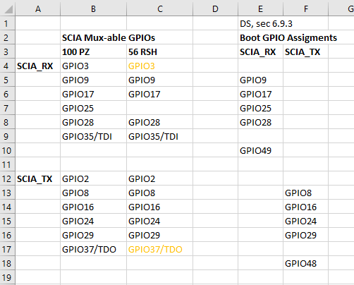
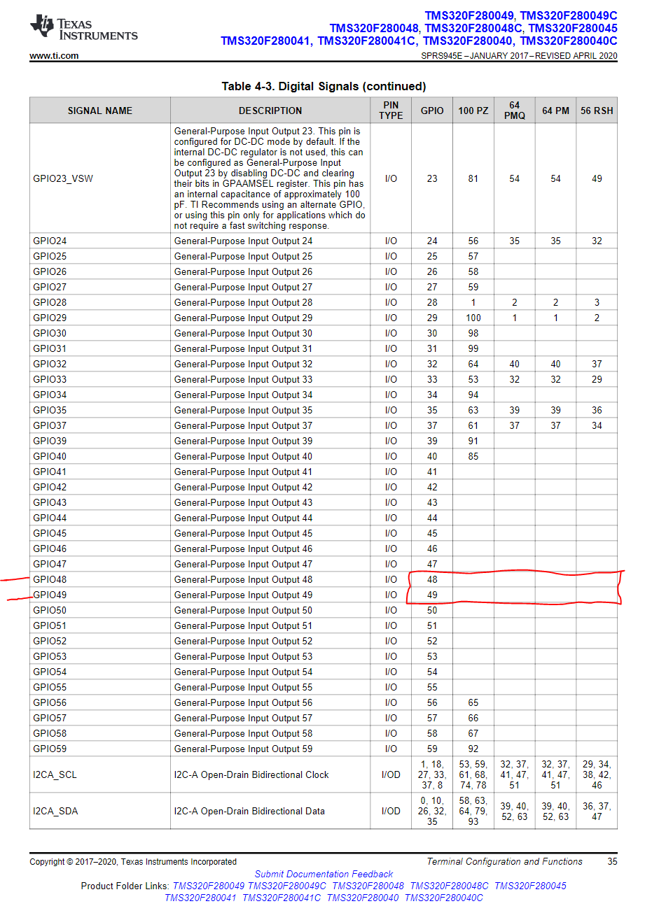
One thing that is odd to me is why am I able to select GPIO48/49 as GPIO-pins for the SCI boot option, when indeed those GPIOs do not connect to any pins on any package offering of this device?:
One possible workaround I've thought of, to keep from having to build new boards for a bit, is the following:

  1. Change the boot definition to change boot mode '1', as defined by BMSP1/0.  I would change this from SCI-boot, to FLASH-boot, with a different entry point for FLASH (versus boot-mode '3':  normal mode)
  2. Create a semi-custom version of the boot kernel that knows to use the pins I have selected for SCIA, and sets the pin-mux accordingly
  3. Store this custom kernel at the different FLASH entry point from step-1
  4. Now when I select boot-mode-1, it boots the serial boot kernel and uses the right SCIA pins for my application, and I can boot-load over serial.  The main problem I see with this is that I may not be able to use the same process/tools on the host side, since the kernel will already be running, and this isn't expected with the provided host-side tools.

Does this seem viable?

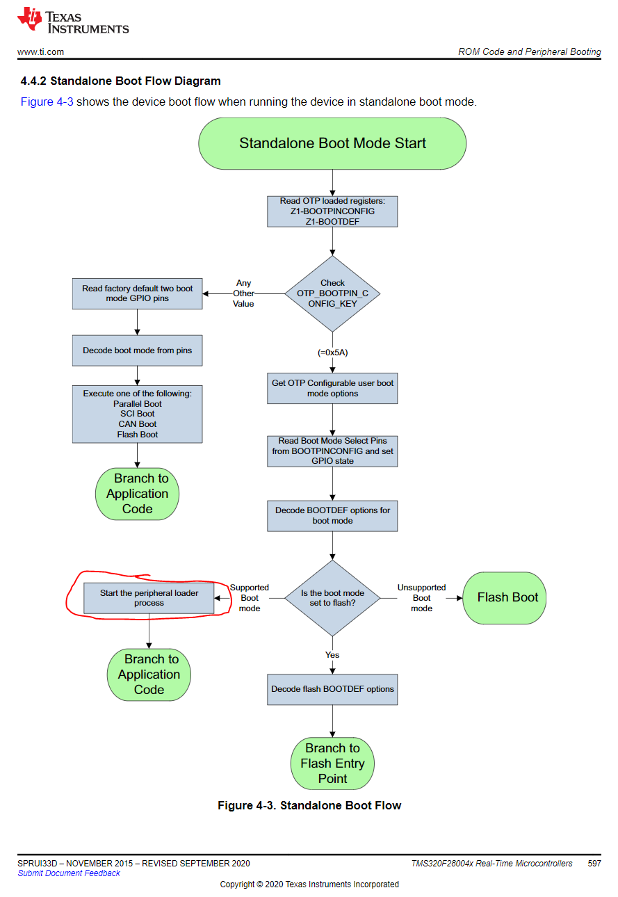
Another similar option I thought of is to simply place a small amount of code at the altered FLASH entry point as mentioned in setp-1 above; this code would simply set up the pin-mux appropriately for my SCIA pin connections.  After doing that, it would jump directly to the serial boot-loader process.  However, I don't know the address of where this process starts.  Is there a way to figure out the address of the circled process, so that the entire boot process doesn't restart after I have changed the pin-mux?:

Thanks for any confirmations or suggestions!

Ted

  • Hi Ted,

    Thanks for the question! I will start by saying I will look into the reasoning for having the GPIO48/49 in the SCI Boot Options table, as this may be an artifact of legacy devices. If it is, we will make sure to remove this in the next revision!

    Now regarding the first boot process: assuming I am not missing any information here, I do think this is viable. The main hurdles will be developing the custom SCI-loader kernel, and then (like you said) the host-side handshake intricacies.

    Regarding the entry point, if I am understanding your reasoning behind it, then I think what you are looking for is essentially _c_int00 which is the startup routine name in C, with its associated address. The linker file has this information, and you can define a custom entry point as outlined in chapter "3.2 Entry Point" of the TMS320C28x Assembly Language Tools User's Guide. Essentially it will come down to the linker file though. Let me know if this is not what you meant by this though!

    Thanks again for your questions, and let me know if this helped answer them!

    Regards,

    Vince

    ----------------------------------------------------------------------------------------------------------------------------

    If I was able to answer your question, please press the green "Verified" button below, thanks!

  • Hi Vince,

    Thanks for looking into this!

    I'm the hardware guy on this project, and after reading your reply and looking more into what it would take for me to generate custom versions of the bootloaders, I decided that was a little bit too ambitious for me.  So I decided to go with a more hardware-oriented approach, and I soldered a couple blue-wires onto my board :-)

    The new workaround involves sticking with standard bootloaders, but utilizing one of the alternate GPIO assignments for the SCIA_RX/TX signals.  I'm using GPIO16 and GPIO17, which turns out to be "Option 1" of the SCI boot mode, and requires a value of 0x21 to be written to the BOOTDEFx register.  I've gone ahead and tested this in emulation mode: with debugger connected, I write to address 0x0000 0D00 the value 0x5AFF 1820, and to address 0x000 0D04 the value 0x2100, and to address 0x0000 0D05 the value 0x0302.  When I set the boot pins appropriately to '01', and reset and run using Code Composer, I am able to use serial_flash_programmer.exe to program the device...great, things are working as expected!

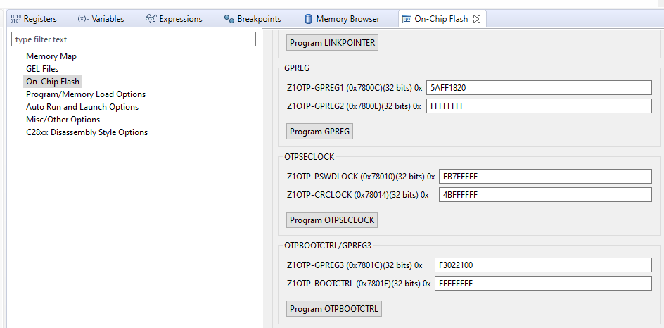
    However, I'm having problems moving into standalone mode and utilizing OTP (i.e. no debugger connected).  What I've done here is go into debugging mode, and in Code Composer, I went to Tools -> On-Chip Flash, and I wrote to two OTP locations:  Z1OTP-GPREG1 (wrote value: 0x5AFF1820), and to Z1OTP-GPREG3 (tried to write value: 0x03022100, but for some reason it won't let me...after I try to write, and then I read it, it shows a value of: 0xF3022100), as shown below.  From my understanding, this should operate just as it did when I had the debugger connected, but it doesn't.  When I disconnect the debugger, power cycle the target board, assert reset, change my boot pins to the same value ('01'), and then deassert reset, I cannot connect to the board using serial_flash_programmer.exe.  What might I be missing and/or have screwed up?

    Thanks!

    Ted


  • Hi Ted,

    Glad to hear about the EMU boot working correctly!

    What is a bit concerning is that GPREG3 OTP isn't letting you write the second value. Would you be able to provide some details on the process used to program the two registers? The reason I ask is that it sounds like GPREG3 was programmed in OTP previously (maybe during one of the steps), which would prevent it from be programmed again. Essentially, if the standalone boot process was emulated at any point, the values that were in OTP at the time were programmed at that point. If that's the case, we'll have to see about a workaround for that.

    Regards,

    Vince

  • Hi Vince,

    The way I went about programming those two OTP registers was directly through that On-Chip Flash window from within CCS.  I did not emulate the standalone boot process at any point.  I do remember before I clicked the buttons to program each register, that they were both set to 0xFFFFFFFF...so they were "fresh".  However, I also remember not paying enough attention when I programmed GPREG3, so it's definitely possible I had a typo before I clicked the program button.  I thought perhaps this area of memory was more like EEPROM, and even though I programmed it once, I could still go back in and change any 1's to 0's (F to a 0), but it sounds like it really gets locked out once you "touch" that register.

    I do have other boards that I'm able to experiment with, but I would like to confirm something first:  That register that is currently set to 0xF3022100 (but should be set to 0x03022100), should that really disallow me from doing what I want to do?  That most-significant-nibble that is in error (F instead of 0), pertains to when I have the BMSP pins set to '11'; boot-to-flash.  Yes, that BOOTDEF value of 0xF3 is an invalid value.  However, when I have the BMSP pins set to '01', why would that invalid value keep me from booting via serial?  The byte in BOOTDEF for mode '01' is valid: 0x21.  I guess it's possible that the 1st level bootloader evaluates the entire BOOTDEF-LOW register, and not just the byte for the currently-selected boot mode, and if it finds an invalid value anywhere in that whole register, it just goes to wait mode?

    Thanks!

    Ted

  • Hi Ted,

    Thanks for the clarification! Unfortunately you are correct that we cannot change any 1's to 0's after programming (our device utilizes one-time-programmable which prevents any changes to the values once programmed, unlike one-time-writable flash memory which allows written 1's to be later programmed to 0's).

    Additionally, to clarify the BOOTDEF behavior, any unsupported boot mode will reset the device.

    So considering the OTP is now written, for your testing in the meantime I would recommend utilizing the emulation boot flow (this will avoid having to set up a new board and program that device's OTP)!

    Regards,

    Vince