This thread has been locked.

If you have a related question, please click the "Ask a related question" button in the top right corner. The newly created question will be automatically linked to this question.

TMS320F28379D: SPI with DMA problem: DMA reads first word wrong

Part Number: TMS320F28379D

Hello dear colleagues,

Have been struggling with that issue for a while, any comments and ideas are highly appreciated.

I have a program that writes and reads data to/ from SPI with DMA. 

DMA init called from main:

/** @brief Configure DMA for channels 5 and 6 */
void initDMA()
{
    DMA_initController();
    // configure DMA CH5
    DMA_configMode(DMA_CH5_BASE, DMA_TRIGGER_SPIBTX, DMA_CFG_ONESHOT_DISABLE | DMA_CFG_SIZE_16BIT | DMA_CFG_CONTINUOUS_DISABLE);
    DMA_enableTrigger(DMA_CH5_BASE);

    // configure DMA CH6
    DMA_configMode(DMA_CH6_BASE, DMA_TRIGGER_SPIBRX, DMA_CFG_ONESHOT_DISABLE | DMA_CFG_SIZE_16BIT | DMA_CFG_CONTINUOUS_DISABLE);
    DMA_enableTrigger(DMA_CH6_BASE);
}

Then another function is called from timer interrupt, which configures DMA channels and starts transfer:

Part of the function dealing with DMA:

This is read from SPI function. Write to SPI function is basically identical except for addresses. 

        // Configure DMA CH5
        EALLOW;
        // Set up SOURCE address.
        HWREG(DMA_CH5_BASE + DMA_O_SRC_BEG_ADDR_SHADOW) = (uint32_t)dummy_var;
        HWREG(DMA_CH5_BASE + DMA_O_SRC_ADDR_SHADOW)     = (uint32_t)dummy_var;
        // Set up DESTINATION address.
        HWREG(DMA_CH5_BASE + DMA_O_DST_BEG_ADDR_SHADOW) = (SPIB_BASE + SPI_O_TXBUF);
        HWREG(DMA_CH5_BASE + DMA_O_DST_ADDR_SHADOW)     = (SPIB_BASE + SPI_O_TXBUF);
        // Set up BURST registers.
        HWREGH(DMA_CH5_BASE + DMA_O_BURST_SIZE)     = 0;
        HWREGH(DMA_CH5_BASE + DMA_O_SRC_BURST_STEP) = 0;
        HWREGH(DMA_CH5_BASE + DMA_O_DST_BURST_STEP) = 0;
        // Set up TRANSFER registers.
        HWREGH(DMA_CH5_BASE + DMA_O_TRANSFER_SIZE)     = len_w + len_dummy_w - 1U;
        HWREGH(DMA_CH5_BASE + DMA_O_SRC_TRANSFER_STEP) = 0;
        HWREGH(DMA_CH5_BASE + DMA_O_DST_TRANSFER_STEP) = 0;
        // Start DMA channel
        HWREGH(DMA_CH5_BASE + DMA_O_CONTROL) |= DMA_CONTROL_RUN;

        // Configure DMA CH6
        // Set up SOURCE address.
        HWREG(DMA_CH6_BASE + DMA_O_SRC_BEG_ADDR_SHADOW) = (SPIB_BASE + SPI_O_RXBUF);
        HWREG(DMA_CH6_BASE + DMA_O_SRC_ADDR_SHADOW)     = (SPIB_BASE + SPI_O_RXBUF);
        // Set up DESTINATION address.
        HWREG(DMA_CH6_BASE + DMA_O_DST_BEG_ADDR_SHADOW) = (uint32_t)rx_buf.p_rx_pckt;
        HWREG(DMA_CH6_BASE + DMA_O_DST_ADDR_SHADOW)     = (uint32_t)rx_buf.p_rx_pckt;
        // Set up BURST registers.
        HWREGH(DMA_CH6_BASE + DMA_O_BURST_SIZE)     = 0;
        HWREGH(DMA_CH6_BASE + DMA_O_SRC_BURST_STEP) = 0;
        HWREGH(DMA_CH6_BASE + DMA_O_DST_BURST_STEP) = 1;
        // Set up TRANSFER registers.
        HWREGH(DMA_CH6_BASE + DMA_O_TRANSFER_SIZE)     = len_w + len_dummy_w - 1U;
        HWREGH(DMA_CH6_BASE + DMA_O_SRC_TRANSFER_STEP) = 0;
        HWREGH(DMA_CH6_BASE + DMA_O_DST_TRANSFER_STEP) = 1;
        // Start DMA channel
//        SysCtl_delay(9);                        // TODO: Doesn't work with smaller delay?!?!?!?
        DMA_isBaseValid(DMA_CH6_BASE);
        HWREGH(DMA_CH6_BASE + DMA_O_CONTROL) |= DMA_CONTROL_RUN;
        // Start transfer
        HWREGH(DMA_CH5_BASE + DMA_O_CONTROL) |= DMA_CONTROL_PERINTFRC;
        EDIS;

Please notice lines 5 and 6 from the bottom. The program works as expected when delay is >= 9 or when DMA_isBaseValid() function is called. Basically same code from send function works fine even without delay. Both send and receive buffers are in the same code section.

DMA is stopped from another function: 

(excerpt)

    // Stop DMA CH5 and CH6
    EALLOW;
    HWREGH(DMA_CH5_BASE + DMA_O_CONTROL) |= DMA_CONTROL_HALT;
    HWREGH(DMA_CH6_BASE + DMA_O_CONTROL) |= DMA_CONTROL_HALT;
    EDIS;

I have to reinitialize DMA every time because I use the same channels for write and read.

Expected behaviour: 
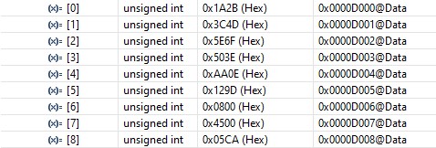
All the data is correct, starts from x[0]. This is the result of the program with added delay.

How it works without delay:
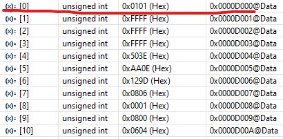
Data under the red line is correct, but should start from x[0], so basically it's shifted in memory. Data x[0] is some random data, changing sometimes.

This behaviour is stable and DMA always starts to write data exactly 1 address higher then it should. 

When I add delay, the first transfer is incorrect (it also starts from the same +1 address), but afterwards all the transfers are correct. As I mentioned earlier, it doesn't happen with sending data to SPI, although it's basically the same code.

I thought it might be SPI shifting the first word wrong of smth. I checked the data with logic analyzer and the incoming data is correct and has no additional word. Also both diagrams from logic analyzer (correct and incorrect operation) look identical, including time between transfers etc. So I suppose it's actually not a problem of DMA but somehow SPI.

I also don't reconfigure SPI before DMA transfer, and also didn't find anything in datasheet about necessary delays after configuring DMA.

My SPI configuration:

void
init_spib_master(void)
{
    // Put SPI into reset before configuring it
    SPI_disableModule(SPIB_BASE);

    // SPI configuration. Use a 40MHz SPICLK and 16-bit word size.
    SPI_setConfig(SPIB_BASE, DEVICE_LSPCLK_FREQ, SPI_PROT_POL0PHA1,
                  SPI_MODE_MASTER, 40000000, 16);
    SPI_enableHighSpeedMode(SPIB_BASE);
    SPI_disableLoopback(SPIB_BASE);
    SPI_setEmulationMode(SPIB_BASE, SPI_EMULATION_FREE_RUN);

    // FIFO configuration for DMA
    SPI_enableFIFO(SPIB_BASE);
    SPI_clearInterruptStatus(SPIB_BASE, SPI_INT_RXFF | SPI_INT_TXFF);
    SPI_setFIFOInterruptLevel(SPIB_BASE, SPI_FIFO_TX1, SPI_FIFO_RX1);

    // Enable SPI module.
    SPI_enableModule(SPIB_BASE);
}

This is of course a small delay and doesn't really matter in that case, so I could just leave it, but I want to find out a reason for it. Maybe I should check some register instead and wait for some flag to be set etc. That way it is more reliable. 

Please let me know if you have any ideas.

Best regards,

Ivan.


  • Hello Ivan,

    You may need to resend your images, they did not come across. Some questions/clarifications:

    Ivan Minakov1 said:
    This is read from SPI function. Write to SPI function is basically identical except for addresses. 

    I see CH5 writing to SPI and CH6 reading from SPI. Is this what you meant? 

    CH5 reads from the same dummy_var and writes to the SPI TX register. 

    CH6 reads from SPI RX register and writes to rx_buf.

    Ivan Minakov1 said:
    Please notice lines 5 and 6 from the bottom. The program works as expected when delay is >= 9 or when DMA_isBaseValid() function is called. Basically same code from send function works fine even without delay. Both send and receive buffers are in the same code section.

    Here you mention a "send buffer", but I only see you reading from dummy_var, which I assume is not actually a buffer.

    Ivan Minakov1 said:
    I thought it might be SPI shifting the first word wrong of smth. I checked the data with logic analyzer and the incoming data is correct and has no additional word. Also both diagrams from logic analyzer (correct and incorrect operation) look identical, including time between transfers etc. So I suppose it's actually not a problem of DMA but somehow SPI.

    You images didn't come through, so I can't see what you expect vs. what you receive. Given that the SPI is setup a master and loopback is disabled, I assume the SPI is receiving data from some external source. Is this correct? Or do you have an external loopback connection?

  • Also, could you try configuring and starting CH6 (SPI RX) *before* CH5 (SPI TX)?

  • Hello, Gus! 

    Thank you for the prompt reply!

    Gus Martinez said:
    You images didn't come through, so I can't see what you expect vs. what you receive. Given that the SPI is setup a master and loopback is disabled, I assume the SPI is receiving data from some external source. Is this correct? Or do you have an external loopback connection?

    Sorry, I fixed the images.

    Gus Martinez said:

    I see CH5 writing to SPI and CH6 reading from SPI. Is this what you meant? 

    CH5 reads from the same dummy_var and writes to the SPI TX register. 

    CH6 reads from SPI RX register and writes to rx_buf.

    Basically, I have an external SPI device (KSZ8851SNL) to which I send and receive data from. So I have two buffers, tx_buf and rx_buf. 

    Send function writes data to SPI from tx_buf with DMA CH5 and reads dummy data from SPI with DMA CH6 into a dummy_var. 

    Receive function writes 0x00 data to SPI from dummy_var with DMA CH5 and reads data from SPI with DMA CH6 into rx_buf.

    In both cases DMA is configured identical, except for addresses. Send function works correctly and receive function works only with added delay.

  • If I configure CH6 first, the data is always shifted as before, regardless of delay (tried 9, 90, 500, 5000):

            EALLOW;
            // Configure DMA CH6
            // Set up SOURCE address.
            HWREG(DMA_CH6_BASE + DMA_O_SRC_BEG_ADDR_SHADOW) = (SPIB_BASE + SPI_O_RXBUF);
            HWREG(DMA_CH6_BASE + DMA_O_SRC_ADDR_SHADOW)     = (SPIB_BASE + SPI_O_RXBUF);
            // Set up DESTINATION address.
            HWREG(DMA_CH6_BASE + DMA_O_DST_BEG_ADDR_SHADOW) = (uint32_t)rx_buf.p_rx_pckt;
            HWREG(DMA_CH6_BASE + DMA_O_DST_ADDR_SHADOW)     = (uint32_t)rx_buf.p_rx_pckt;
            // Set up BURST registers.
            HWREGH(DMA_CH6_BASE + DMA_O_BURST_SIZE)     = 0;
            HWREGH(DMA_CH6_BASE + DMA_O_SRC_BURST_STEP) = 0;
            HWREGH(DMA_CH6_BASE + DMA_O_DST_BURST_STEP) = 1;
            // Set up TRANSFER registers.
            HWREGH(DMA_CH6_BASE + DMA_O_TRANSFER_SIZE)     = len_w + len_dummy_w - 1U;
            HWREGH(DMA_CH6_BASE + DMA_O_SRC_TRANSFER_STEP) = 0;
            HWREGH(DMA_CH6_BASE + DMA_O_DST_TRANSFER_STEP) = 1;
            // Start DMA channel
            SysCtl_delay(5000);                        // TODO: Doesn't work with smaller delay?!?!?!?
    //        DMA_isBaseValid(DMA_CH6_BASE);
            HWREGH(DMA_CH6_BASE + DMA_O_CONTROL) |= DMA_CONTROL_RUN;
    
            // Configure DMA CH5
    //        EALLOW;
            // Set up SOURCE address.
            HWREG(DMA_CH5_BASE + DMA_O_SRC_BEG_ADDR_SHADOW) = (uint32_t)dummy_var;
            HWREG(DMA_CH5_BASE + DMA_O_SRC_ADDR_SHADOW)     = (uint32_t)dummy_var;
            // Set up DESTINATION address.
            HWREG(DMA_CH5_BASE + DMA_O_DST_BEG_ADDR_SHADOW) = (SPIB_BASE + SPI_O_TXBUF);
            HWREG(DMA_CH5_BASE + DMA_O_DST_ADDR_SHADOW)     = (SPIB_BASE + SPI_O_TXBUF);
            // Set up BURST registers.
            HWREGH(DMA_CH5_BASE + DMA_O_BURST_SIZE)     = 0;
            HWREGH(DMA_CH5_BASE + DMA_O_SRC_BURST_STEP) = 0;
            HWREGH(DMA_CH5_BASE + DMA_O_DST_BURST_STEP) = 0;
            // Set up TRANSFER registers.
            HWREGH(DMA_CH5_BASE + DMA_O_TRANSFER_SIZE)     = len_w + len_dummy_w - 1U;
            HWREGH(DMA_CH5_BASE + DMA_O_SRC_TRANSFER_STEP) = 0;
            HWREGH(DMA_CH5_BASE + DMA_O_DST_TRANSFER_STEP) = 0;
            // Start DMA channel
            HWREGH(DMA_CH5_BASE + DMA_O_CONTROL) |= DMA_CONTROL_RUN;
    
    
            // Start transfer
            HWREGH(DMA_CH5_BASE + DMA_O_CONTROL) |= DMA_CONTROL_PERINTFRC;
            EDIS;

  • Hello Ivan,

    Thank for clarifying those questions. I understand your issue better now. 

    I've been thinking about your observations. I'm not quite sure what is happening here, but maybe it has something to do with the way you are triggering the DMA.

    In the receive code, I see you are forcing the first CH5 transfer. Would you be able to check the content of x[0] right before you force the first CH5 transfer? If the content of x[0] has already changed, then this would tell us CH6 has already kicked off the first transfer and then we would need to figure out why that is.

    You may want to put a while(1) right before the trigger vs. a breakpoint, just to make sure halting program execution doesn't have an effect on the actual behavior of the problem.

  • Hello, Gus,

    Thank you for the reply! I tried to put while(1) as you said and the contents of x[0] do actually change to 0x0101 before I trigger a transfer! Do you have any idea why could that be?

    Kind regards,

    Ivan.

  • I also tried to activate both channels one after another, CH6 first, CH5 second and the other way around, but the problem persists. 

            // Start DMA channel
            HWREGH(DMA_CH6_BASE + DMA_O_CONTROL) |= DMA_CONTROL_RUN;
            HWREGH(DMA_CH5_BASE + DMA_O_CONTROL) |= DMA_CONTROL_RUN;

  • Hi Ivan,

    It seems that the DMA has received an RX event from the SPI. Can you check the contents of the SPIFFRX register after you configure the SPI and before you enable the DMA channels? It'd be good to know what is the status of the RXFFST and RXFFINT bits. If these bits are non-zero then, for some reason, the SPI has received one or more characters. You may want to try resetting the RX FIFO by calling SPI_resetRxFIFO(). I think you can do it after your call to SPI_setFIFOInterruptLevel().

  • Hello, Gus,

    I checked the SPIFFRX registers. RXFFST is 0x00 and RXFFINT is 1.

    Here is what I tried:

    1. Adding SPI_resetRxFIFO() as you suggested - no effect

    2. Adding SPI_resetRxFIFO() right before DMA init - no effect

    3. Adding SPI_resetRxFIFO() (here I used a HWREG version of it though, not a function) before force trigger - no effect

    4. Clearing RXFFINT before force trigger - no effect

    5. Doing both 3 and 4 - no effect

    What I noticed is that right after I enable DMA CH6

            // Start DMA channel
            HWREGH(DMA_CH6_BASE + DMA_O_CONTROL) |= DMA_CONTROL_RUN;

    The contents of SPIRXBUF and x[0] are both 0x0101 - always that same wrong number (at least at that first transfer, later it changes). I checked it with while(1); technique. Also as I mentioned before that data is not present on logic analyzer.

    I also tried to reset FIFO and clear interrupt flag before enabling CH6. In that case the behaviour is still the same (wrong 1st transfer), but the number is different (0x8000). If I just clear interrupt flag the number is still the same 0x0101.

    Here is a snippet from my test code:

    // Set up TRANSFER registers.
            HWREGH(DMA_CH6_BASE + DMA_O_TRANSFER_SIZE)     = len_w + len_dummy_w - 1U;
            HWREGH(DMA_CH6_BASE + DMA_O_SRC_TRANSFER_STEP) = 0;
            HWREGH(DMA_CH6_BASE + DMA_O_DST_TRANSFER_STEP) = 1;
    
    //        SysCtl_delay(9);                        // TODO: Doesn't work with smaller delay?!?!?!?
    //        while(1);
    
            EDIS;
    
            // Reset the RX FIFO.
            //
            HWREGH(SPIB_BASE + SPI_O_FFRX) &= ~SPI_FFRX_RXFIFORESET;
            HWREGH(SPIB_BASE + SPI_O_FFRX) |= SPI_FFRX_RXFIFORESET;
    
            // Clear interrupt flag
            HWREGH(SPIB_BASE + SPI_O_FFRX) |= SPI_FFRX_RXFFINTCLR;
    
    
    //        while(1);
    
            EALLOW;
            // Start DMA channel
            HWREGH(DMA_CH6_BASE + DMA_O_CONTROL) |= DMA_CONTROL_RUN;
    
            while(1);
    
            // Start transfer
            HWREGH(DMA_CH5_BASE + DMA_O_CONTROL) |= DMA_CONTROL_PERINTFRC;
            EDIS;

  • Ivan,

    Ivan Minakov1 said:
    I checked the SPIFFRX registers. RXFFST is 0x00 and RXFFINT is 1.

    It's odd that the RXFFINT bit is set. Can you post the full contents of the SPIFFRX register? Or maybe it's better to post all the SPI register contents. 

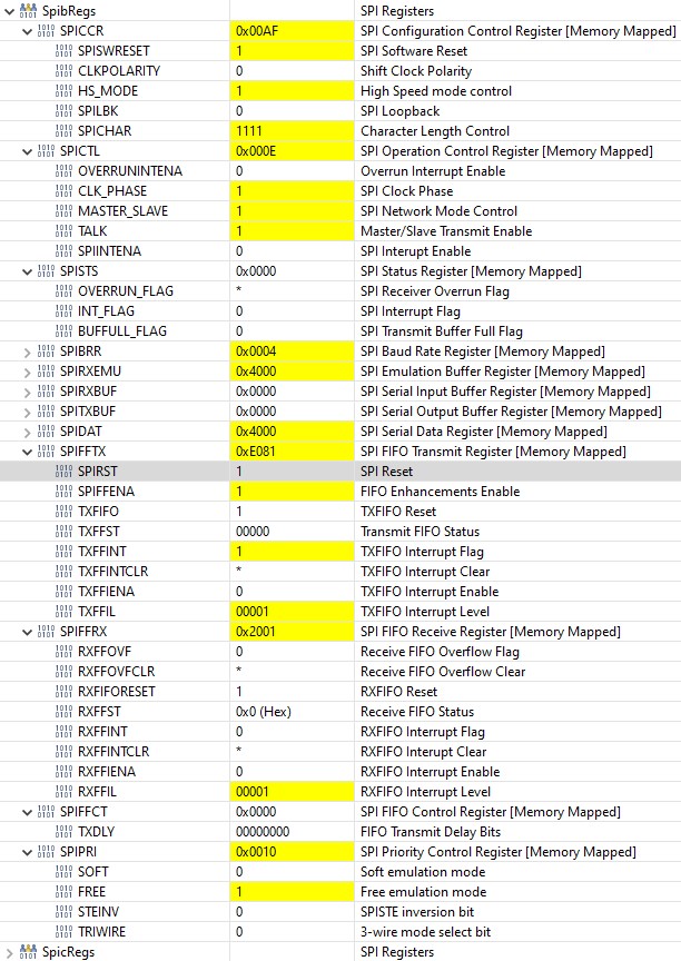
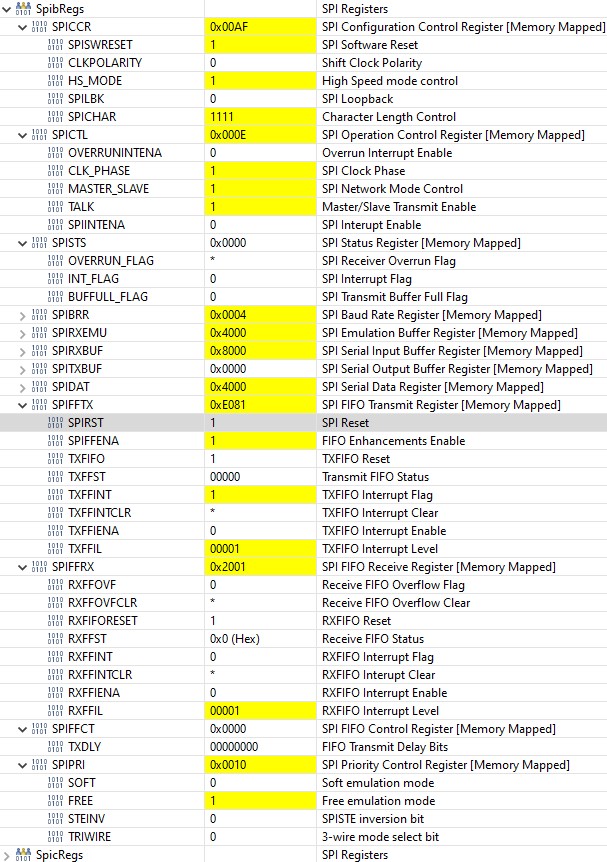
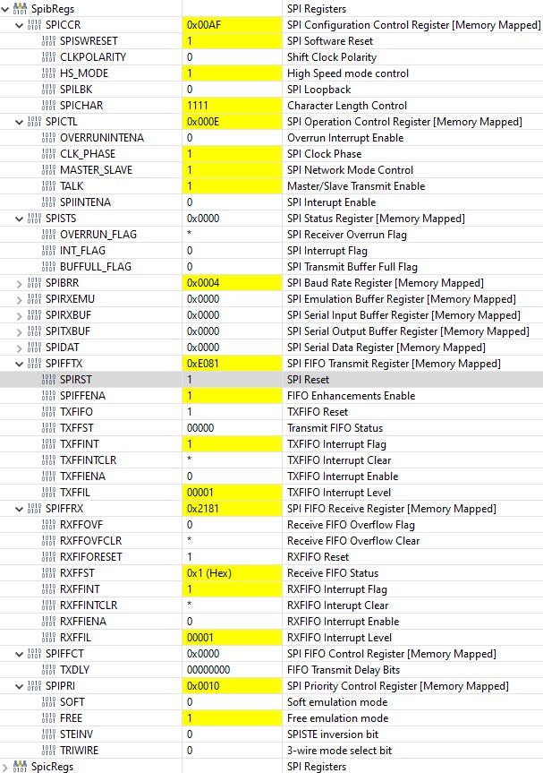
  • Gus, here are the contents of all SPI registers:

    1. Before starting CH5

    2. Before starting CH6

    3. Before force trigger CH5

    4. After force trigger CH5

    Test code:

            // Configure DMA CH5
            EALLOW;
            // Set up SOURCE address.
            HWREG(DMA_CH5_BASE + DMA_O_SRC_BEG_ADDR_SHADOW) = (uint32_t)dummy_var;
            HWREG(DMA_CH5_BASE + DMA_O_SRC_ADDR_SHADOW)     = (uint32_t)dummy_var;
            // Set up DESTINATION address.
            HWREG(DMA_CH5_BASE + DMA_O_DST_BEG_ADDR_SHADOW) = (SPIB_BASE + SPI_O_TXBUF);
            HWREG(DMA_CH5_BASE + DMA_O_DST_ADDR_SHADOW)     = (SPIB_BASE + SPI_O_TXBUF);
            // Set up BURST registers.
            HWREGH(DMA_CH5_BASE + DMA_O_BURST_SIZE)     = 0;
            HWREGH(DMA_CH5_BASE + DMA_O_SRC_BURST_STEP) = 0;
            HWREGH(DMA_CH5_BASE + DMA_O_DST_BURST_STEP) = 0;
            // Set up TRANSFER registers.
            HWREGH(DMA_CH5_BASE + DMA_O_TRANSFER_SIZE)     = len_w + len_dummy_w - 1U;
            HWREGH(DMA_CH5_BASE + DMA_O_SRC_TRANSFER_STEP) = 0;
            HWREGH(DMA_CH5_BASE + DMA_O_DST_TRANSFER_STEP) = 0;
    
    //        while(1);
    
            // Start DMA channel
            HWREGH(DMA_CH5_BASE + DMA_O_CONTROL) |= DMA_CONTROL_RUN;
    
            // Configure DMA CH6
            // Set up SOURCE address.
            HWREG(DMA_CH6_BASE + DMA_O_SRC_BEG_ADDR_SHADOW) = (SPIB_BASE + SPI_O_RXBUF);
            HWREG(DMA_CH6_BASE + DMA_O_SRC_ADDR_SHADOW)     = (SPIB_BASE + SPI_O_RXBUF);
            // Set up DESTINATION address.
            HWREG(DMA_CH6_BASE + DMA_O_DST_BEG_ADDR_SHADOW) = (uint32_t)rx_buf.p_rx_pckt;
            HWREG(DMA_CH6_BASE + DMA_O_DST_ADDR_SHADOW)     = (uint32_t)rx_buf.p_rx_pckt;
            // Set up BURST registers.
            HWREGH(DMA_CH6_BASE + DMA_O_BURST_SIZE)     = 0;
            HWREGH(DMA_CH6_BASE + DMA_O_SRC_BURST_STEP) = 0;
            HWREGH(DMA_CH6_BASE + DMA_O_DST_BURST_STEP) = 1;
            // Set up TRANSFER registers.
            HWREGH(DMA_CH6_BASE + DMA_O_TRANSFER_SIZE)     = len_w + len_dummy_w - 1U;
            HWREGH(DMA_CH6_BASE + DMA_O_SRC_TRANSFER_STEP) = 0;
            HWREGH(DMA_CH6_BASE + DMA_O_DST_TRANSFER_STEP) = 1;
    
    //        while(1);
    
            // Start DMA channel
            HWREGH(DMA_CH6_BASE + DMA_O_CONTROL) |= DMA_CONTROL_RUN;
    
    //        while(1);
    
            // Start transfer
            HWREGH(DMA_CH5_BASE + DMA_O_CONTROL) |= DMA_CONTROL_PERINTFRC;
            EDIS;
    
            while(1);

  • Basically in cases 1-3 contents of registers are identical, and in case 4 the difference is SPIRXEMU, SPIRXBUF, SPIDAT and SPIFFRX.

  • Hello Ivan, 

    Did you remove the instructions to reset the RX FIFO and interrupt flag? My apologies, I should have been clearer that the goal here was to see if those two instructions were having an effect on the RXFFINT flag. My guess is that it is because this flag is set at the time you enable the DMA, you get that extra DMA transfer at the beginning.

    Can you add the instructions to clear the RX FIFO and interrupt flag and capture the status of the SPI registers?

  • I still had a reset FIFO instruction inside the init function:

        ...
        // FIFO configuration for DMA
        SPI_enableFIFO(SPIB_BASE);
        SPI_clearInterruptStatus(SPIB_BASE, SPI_INT_RXFF | SPI_INT_TXFF);
        SPI_setFIFOInterruptLevel(SPIB_BASE, SPI_FIFO_TX1, SPI_FIFO_RX1);
    
        // Reset FIFO
        SPI_resetRxFIFO(SPIB_BASE);
        ...

    Here are the results when I insert reset before starting CH6:

    Code:

            ...
            // Set up TRANSFER registers.
            HWREGH(DMA_CH6_BASE + DMA_O_TRANSFER_SIZE)     = len_w + len_dummy_w - 1U;
            HWREGH(DMA_CH6_BASE + DMA_O_SRC_TRANSFER_STEP) = 0;
            HWREGH(DMA_CH6_BASE + DMA_O_DST_TRANSFER_STEP) = 1;
    
            EDIS;
    
            // Reset the RX FIFO.
            //
            HWREGH(SPIB_BASE + SPI_O_FFRX) &= ~SPI_FFRX_RXFIFORESET;
            HWREGH(SPIB_BASE + SPI_O_FFRX) |= SPI_FFRX_RXFIFORESET;
    
            // Clear interrupt flag
            HWREGH(SPIB_BASE + SPI_O_FFRX) |= SPI_FFRX_RXFFINTCLR;
    
    //        while(1);
    
            EALLOW;
            // Start DMA channel
            HWREGH(DMA_CH6_BASE + DMA_O_CONTROL) |= DMA_CONTROL_RUN;
    
    //        while(1);
    
            // Start transfer
            HWREGH(DMA_CH5_BASE + DMA_O_CONTROL) |= DMA_CONTROL_PERINTFRC;
            EDIS;
    
            while(1);
            ...

    1. Before starting CH6

    2. Before force trigger CH5

    3. After force trigger CH5

  • Results after case 3:

    The data x[0] is still wrong, but the number is now 0x0000 instead of 0x0101.

  • OK, here is my theory on what happened in the original code you posted, at the very beginning of this thread.

    1. You programmed DMA CH5 and enabled it (set RUN bit). Since SPI TXFFINT is set (TXFFST < TXFFIL), the DMA will immediately get triggered and start to move data to the SPI TX FIFO. Note: Your forced trigger of CH5 later probably doesn't have any real effect. 
    2. You then programmed DMA CH6 and enabled it (set RUN bit). Since SPI RXFFINT is set (based on experiments above where you didn't explicitly clear the RXFFINT flag bit), the DMA will immediately get triggered and start moving data from the SPI RX FIFO. Note: the CPU is much faster than the SPI. In all likelihood the SPI still hasn't finished transmitting the first character by this point. Therefore DMA CH6 will just pick up whatever is in the SPI RX FIFO at that time. At this point DMA CH6 has jumped head of CH5 by one character, causing the offset in your data buffer.

    Why does the delay matter? Because you are giving the SPI time to finish the first transfer. Therefore, by the time you enable CH6, you have a valid value in the SPI RX FIFO.

    How to solve the problem:

    • Make sure you clear the RXFFINT flag *before* you enable CH6. 
    • Do not force trigger CH5. I bet the fact that TXFFINT is set will cause the Ch5 to trigger as soon as you "RUN" CH5.
    • Enable (set RUN) CH5 & CH6 closer together. Or at least make sure CH6 is enabled first.

  • Hello Gus,

    thank you for the explanation, it makes perfect sence to me, but the problem persists. I followed your advice and here is how the code looks like now:

            // Configure DMA CH5
            EALLOW;
            // Set up SOURCE address.
            HWREG(DMA_CH5_BASE + DMA_O_SRC_BEG_ADDR_SHADOW) = (uint32_t)dummy_var;
            HWREG(DMA_CH5_BASE + DMA_O_SRC_ADDR_SHADOW)     = (uint32_t)dummy_var;
            // Set up DESTINATION address.
            HWREG(DMA_CH5_BASE + DMA_O_DST_BEG_ADDR_SHADOW) = (SPIB_BASE + SPI_O_TXBUF);
            HWREG(DMA_CH5_BASE + DMA_O_DST_ADDR_SHADOW)     = (SPIB_BASE + SPI_O_TXBUF);
            // Set up BURST registers.
            HWREGH(DMA_CH5_BASE + DMA_O_BURST_SIZE)     = 0;
            HWREGH(DMA_CH5_BASE + DMA_O_SRC_BURST_STEP) = 0;
            HWREGH(DMA_CH5_BASE + DMA_O_DST_BURST_STEP) = 0;
            // Set up TRANSFER registers.
            HWREGH(DMA_CH5_BASE + DMA_O_TRANSFER_SIZE)     = len_w + len_dummy_w - 1U;
            HWREGH(DMA_CH5_BASE + DMA_O_SRC_TRANSFER_STEP) = 0;
            HWREGH(DMA_CH5_BASE + DMA_O_DST_TRANSFER_STEP) = 0;
    
    
            // Configure DMA CH6
            // Set up SOURCE address.
            HWREG(DMA_CH6_BASE + DMA_O_SRC_BEG_ADDR_SHADOW) = (SPIB_BASE + SPI_O_RXBUF);
            HWREG(DMA_CH6_BASE + DMA_O_SRC_ADDR_SHADOW)     = (SPIB_BASE + SPI_O_RXBUF);
            // Set up DESTINATION address.
            HWREG(DMA_CH6_BASE + DMA_O_DST_BEG_ADDR_SHADOW) = (uint32_t)rx_buf.p_rx_pckt;
            HWREG(DMA_CH6_BASE + DMA_O_DST_ADDR_SHADOW)     = (uint32_t)rx_buf.p_rx_pckt;
            // Set up BURST registers.
            HWREGH(DMA_CH6_BASE + DMA_O_BURST_SIZE)     = 0;
            HWREGH(DMA_CH6_BASE + DMA_O_SRC_BURST_STEP) = 0;
            HWREGH(DMA_CH6_BASE + DMA_O_DST_BURST_STEP) = 1;
            // Set up TRANSFER registers.
            HWREGH(DMA_CH6_BASE + DMA_O_TRANSFER_SIZE)     = len_w + len_dummy_w - 1U;
            HWREGH(DMA_CH6_BASE + DMA_O_SRC_TRANSFER_STEP) = 0;
            HWREGH(DMA_CH6_BASE + DMA_O_DST_TRANSFER_STEP) = 1;
    
            EDIS;
    
            // Clear interrupt flag
            HWREGH(SPIB_BASE + SPI_O_FFRX) |= SPI_FFRX_RXFFINTCLR;
    
            EALLOW;
            // Start DMA CH6
            HWREGH(DMA_CH6_BASE + DMA_O_CONTROL) |= DMA_CONTROL_RUN;
    
            // Start DMA CH5
            HWREGH(DMA_CH5_BASE + DMA_O_CONTROL) |= DMA_CONTROL_RUN;
    
            // Start transfer
    //        HWREGH(DMA_CH5_BASE + DMA_O_CONTROL) |= DMA_CONTROL_PERINTFRC;
            EDIS;

    If I don't force trigger CH5, only the first false word is transferred (x[0] = 0x0101), if I do force trigger, the full transfer is happening and the data looks shifted as before and the x[0] is 0x0101 as before.

  • Also if I stop right after enabling CH6 and before enabling CH5, the first transfer already occurs and x[0] = 0x0101.

  • Hello Ivan,

    So it looks like the CH6 got triggered somehow. Can you check the status of PERINTFLG on CH6 before you enable it? If it's set, then maybe that's the reason. There is a PERINTCLR bit which you can use to clear that bit before you enable CH6. 

  • Gus, 

    I went through my code again and found that before I stop DMA CH5 and CH6 I already send a couple of control words via SPI. That set flags in SPI and DMA and also filled RX FIFO. That was one of the problems, but the second one, why x[0] was wrong had to do with PERINTCLR. That was basically the biggest change compared to the original code. 

    Thank you very much for your time and effort! I really appreciate it.

    Final code:

            // Setup DMA
            EALLOW;
            // Configure DMA CH5
            // Set up SOURCE address.
            HWREG(DMA_CH5_BASE + DMA_O_SRC_BEG_ADDR_SHADOW) = (uint32_t)dummy_var;
            HWREG(DMA_CH5_BASE + DMA_O_SRC_ADDR_SHADOW)     = (uint32_t)dummy_var;
            // Set up DESTINATION address.
            HWREG(DMA_CH5_BASE + DMA_O_DST_BEG_ADDR_SHADOW) = (SPIB_BASE + SPI_O_TXBUF);
            HWREG(DMA_CH5_BASE + DMA_O_DST_ADDR_SHADOW)     = (SPIB_BASE + SPI_O_TXBUF);
            // Set up BURST registers.
            HWREGH(DMA_CH5_BASE + DMA_O_BURST_SIZE)     = 0;
            HWREGH(DMA_CH5_BASE + DMA_O_SRC_BURST_STEP) = 0;
            HWREGH(DMA_CH5_BASE + DMA_O_DST_BURST_STEP) = 0;
            // Set up TRANSFER registers.
            HWREGH(DMA_CH5_BASE + DMA_O_TRANSFER_SIZE)     = len_w + len_dummy_w - 1U;
            HWREGH(DMA_CH5_BASE + DMA_O_SRC_TRANSFER_STEP) = 0;
            HWREGH(DMA_CH5_BASE + DMA_O_DST_TRANSFER_STEP) = 0;
    
            // Configure DMA CH6
            // Set up SOURCE address.
            HWREG(DMA_CH6_BASE + DMA_O_SRC_BEG_ADDR_SHADOW) = (SPIB_BASE + SPI_O_RXBUF);
            HWREG(DMA_CH6_BASE + DMA_O_SRC_ADDR_SHADOW)     = (SPIB_BASE + SPI_O_RXBUF);
            // Set up DESTINATION address.
            HWREG(DMA_CH6_BASE + DMA_O_DST_BEG_ADDR_SHADOW) = (uint32_t)rx_buf.p_rx_pckt;
            HWREG(DMA_CH6_BASE + DMA_O_DST_ADDR_SHADOW)     = (uint32_t)rx_buf.p_rx_pckt;
            // Set up BURST registers.
            HWREGH(DMA_CH6_BASE + DMA_O_BURST_SIZE)     = 0;
            HWREGH(DMA_CH6_BASE + DMA_O_SRC_BURST_STEP) = 0;
            HWREGH(DMA_CH6_BASE + DMA_O_DST_BURST_STEP) = 1;
            // Set up TRANSFER registers.
            HWREGH(DMA_CH6_BASE + DMA_O_TRANSFER_SIZE)     = len_w + len_dummy_w - 1U;
            HWREGH(DMA_CH6_BASE + DMA_O_SRC_TRANSFER_STEP) = 0;
            HWREGH(DMA_CH6_BASE + DMA_O_DST_TRANSFER_STEP) = 1;
    
            // Clear peripheral interrupt CH6
            HWREGH(DMA_CH6_BASE + DMA_O_CONTROL) |= DMA_CONTROL_PERINTCLR;
            // Start DMA CH6
            HWREGH(DMA_CH6_BASE + DMA_O_CONTROL) |= DMA_CONTROL_RUN;
    
            // Start DMA CH5
            HWREGH(DMA_CH5_BASE + DMA_O_CONTROL) |= DMA_CONTROL_RUN;
    
            // Start transfer
            HWREGH(DMA_CH5_BASE + DMA_O_CONTROL) |= DMA_CONTROL_PERINTFRC;
            EDIS;

    Kind regards,

    Ivan.