This thread has been locked.

If you have a related question, please click the "Ask a related question" button in the top right corner. The newly created question will be automatically linked to this question.

CCS/TMS320F28335: Understanding a block diagram of datasheet issue.

Part Number: TMS320F28335

Tool/software: Code Composer Studio

Hi. I'm using TMS320F28335.

I read the datasheet many time to know how to operate.

But every time, block diagram makes me complicated.
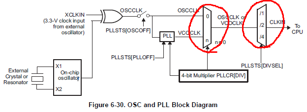
Referring to above two diagram, I accentuate with a red circle.

WDRST with bar. What's the meaning of the bar? Is it 'not'?

What's the meaning of red circles?

I'm poor at reading and understanding the datasheet.

Is there any know-how to understand the block diagram or something like that?

Thank you.

  • Joon,

    I'll try and explain the images in more detail:

    In Fig 6-30 the logic blocks you have circled are showing a logical multiplexer(or mux).  The first one controls the multiplier to the PLL on this device that is used to scale up the input clock frequency.  The output of the mux in this case is controlled by the DIV bits in the PLLCR register.  The next mux controls the PLL divider before the clock is sent to the CPU.  In this case the DIVSEL bits in the PLLSTS register control whether this is a divide by 1(/1) divide by 2 (/2) divide by 4(/4).

    You can refer to the register bit definitions in the F28335 TRM in section 1.3

    For Fig 6-34, this diagram is showing how the internal watchdog module can be used to force a reset to the system via a pulse on the XRSn pin itself.  As you mentioned the "bar" over the signal names indicate that the signal is an active low signal.  So, if enabled, when the watchdog times out it will assert WDRST(bar).  In the lower left of the diagram you can see that this signal will enable the output of a buffer, which in turn drives the XRSn pin low as well as sending this signal to the device.  The internal pullup, is actually and active signal that will keep the XRSn pin inactive high under normal conditions.  I believe we also recommend placing a stronger external pullup on the pin itself to ensure there are not noise coupling that would put the device in reset state.

    Core reset is just the signal that carries the XRSn signal to the rest of the device.

    Best,
    Matthew

  • Thank you very much Matthew.

    Can I add you to my friend? haha...

    Sincerely.