Other Parts Discussed in Thread: CONTROLSUITE
Tool/software: Code Composer Studio
Hi There,
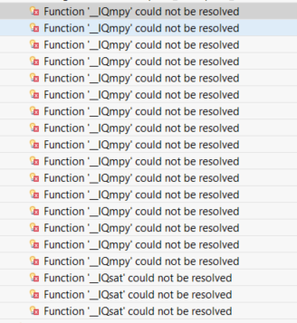
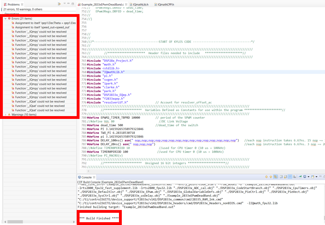
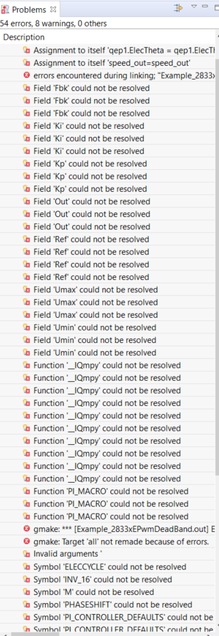
How are you? I am working on an in-house designed controller based on the TMS320F28335 DPS. I am using CCSV8, compiler 6.2.9, to compile the code. The code was tested and working. I have got a new laptop and had to reinstall the CCS, but the working code started giving me errors. Please see the errors and the code attached. Could anyone please suggest where the problem could be? Thank you very much!
/////////////////////////////////////////////////////////////////////////////////////////////////
//        //**********************  Header files needed to include   **********************//
/////////////////////////////////////////////////////////////////////////////////////////////////
#include "DSP28x_Project.h"
#include "math.h"
#include <stdlib.h>
#include "IQmathLib.h"
#include "pi.h"
#include "svgen.h"
#include "ipark.h"
#include "clarke.h"
#include "park.h"
#include "DSP2833x_EQep.h"
#include "f2833xqep.h"
#include "resolverLUT.h"                // Account for resolver_offset_ac
///////////////////////////////////////////////////////////////////////////////////////////////
        //**********************  Variables Defined as Constants for use within the program **********************//
///////////////////////////////////////////////////////////////////////////////////////////////
#define EPWM2_TIMER_TBPRD 10000         // period of the SPWM counter
//#define Vdc 80                          //DC Link Voltage
#define dead_time 500                   //dead_time of the switch
#define PI 3.14159265358979323846
#define TWO_PI 6.28318530718
#define pi 3.14159265358979323846
#define DELAY_100ns() asm(" nop;nop;nop;nop;nop;nop;nop;nop;nop;nop;nop;nop;nop;nop;nop")   //each nop instruction takes 6.67ns. 15 nop ~= 100ns
#define DELAY_20ns() asm(" nop;nop;nop")                                                    //each nop instruction takes 6.67ns. 3 nop ~= 20ns
//#define TIMER0PERIOD 10                 //used for CPU timer 0 (10 us = 100kHz)
#define TIMER0PERIOD 100                 //used for CPU timer 0 (10 us = 100kHz)
//#define PI_MACRO(v)
///////////////////////////////////////////////////////////////////////////////////////////////
        //**********************  Unsigned 16 bit integers **********************//
///////////////////////////////////////////////////////////////////////////////////////////////
Uint16 LoopCount;
Uint16 State;
Uint16 Speed_Control;
Uint16 Encoder_Control;
Uint16 ConversionCount;

///////////////////////////////////////////////////////////////////////////////////////////////
        //**********************  Arrays used for plotting in Debug Mode   **********************//
///////////////////////////////////////////////////////////////////////////////////////////////
float Id[256];
float Iq[256];
float vd[256];
float vq[256];

float current_Test[256];
float Temp;

///////////////////////////////////////////////////////////////////////////////////////////////
//**********************  Arrays used for reading ADC data and current sensor calibration  **********************//
///////////////////////////////////////////////////////////////////////////////////////////////
float currents[6];
const float currentScaling[6] = {1.0,1.0,1.0,0.1234567,0.1234567,0.37};
const float currentOffset[6] = {0.0000,0.0000,0,0.04,0.04,0.04};
const short channelArray[6] = {0,1,2,3,4,5};

///////////////////////////////////////////////////////////////////////////////////////////////
        //**********************  Variables used for transformations, function calls, etc.   **********************//
///////////////////////////////////////////////////////////////////////////////////////////////
float maxDigital_A = 4075.0, minDigital_A = -4075.0, minAnalog_A = -5.0, maxAnalog_A = 5.0; //conversion parameters used for PhaseA
float maxDigital_B = 4070.0, minDigital_B = -4070.0, minAnalog_B = -5.0, maxAnalog_B = 5.0; //conversion parameters used for PhaseB
float maxDigital_C = 8135.0, minDigital_C = -8130.0, minAnalog_C = -5.0, maxAnalog_C = 5.0; //conversion parameters used for PhaseC
float PhaseA, PhaseB, PhaseC, ialpha, ibeta, id, iq, Vd = 0.0, Vq = 0.0, Valpha, Vbeta, dutyA, dutyB, dutyC;  //Variables for Transformations
float PhaseA_Current;
float Theta, Im;                                        //Theta is the rotor angle, Im is the amplitude of the input sine wave
//float Vref_magn, M,
float Ts = 1.0/10000.0;                   //M is modulation index, Ts is sampling period
float id_ref=0 , iq_ref =-0 , rpm_ref ;      //references used for the PI controller
short increment, r;                                     //short counters used for reading the ADC

/* -------- The following three parameters are used for specific formulas for the kp and ki for PI controller ------------ */
float freq_bw = 750;                                    //Has to be less than fsw/10
float L = 0, R = 0;                                     //Inductance and Resistor of the motor

///////////////////////////////////////////////////////////////////////////////////////////////
        //**********************  Variables used for Voltage Open Loop Control   **********************//
///////////////////////////////////////////////////////////////////////////////////////////////
double mm=0;
double tm=0;
float V_test=0;
float N_test=0;
float va=0, vb=0, vc=0;
float V_DC=10;
double kp_id=0.12;
double ki_id=8.57;
double kp_iq=0.132;
double ki_iq=14.25;

///////////////////////////////////////////////////////////////////////////////////////////////
        //**********************  Variables for Speed filtering   **********************//
///////////////////////////////////////////////////////////////////////////////////////////////
int16 count=0;
float pos_out_p, speed_out, speed_mech, speed_est, pos_est, pos_prev, pi_posout_p, speed_out_p, sum, speed_rpm;
Uint16 count_lm=5;
float temps[21];
int n;
int m=3;
int nl=20;
int POLES = 10;
float Encoder_Offset = 0.0;

///////////////////////////////////////////////////////////////////////////////////////////////
//**********************  Creating instances of various struct objects defined in the MACROS   **********************//
///////////////////////////////////////////////////////////////////////////////////////////////
PI_CONTROLLER pi_d = PI_CONTROLLER_DEFAULTS, pi_q = PI_CONTROLLER_DEFAULTS, rpm = PI_CONTROLLER_DEFAULTS;
SVGEN svgen1 = SVGEN_DEFAULTS;
IPARK ipark1 = IPARK_DEFAULTS;
CLARKE clarke1 = CLARKE_DEFAULTS;
PARK park1 = PARK_DEFAULTS;
QEP qep1 = QEP_DEFAULTS;

///////////////////////////////////////////////////////////////////////////////////////////////
        //**********************  Function Prototypes   **********************//
///////////////////////////////////////////////////////////////////////////////////////////////
void InitEPwm1Example(void);
void InitEPwm2Example(void);
void InitEPwm3Example(void);
void InitEPwm5Example(void);
void InitEPwm6Example(void);
void init_XINTF(void);
void ADC_reset(void);
void getPositionAndSpeed_Encoder();
short ADC_readdata(void);
void init_CPU_timers(void);
void init_xinterrupts(void);
void init_DIO(void);
void resolver_reset(void); // Reset the AD2S1205
// Position sensor and calibration
void resolver_readdata(void); // Read resolver data from external zone 6 into memory
const short resolver_offset_dc = RSV_OFFSET_DC; // resolver is physically at an angle of 60 deg. electrical wrt phase A
volatile short resolver_offset_ac = 0;
const float inv_16 = INV_16; // inverse of 16, for resolver_ac_offset table. Table defined by 0:16:4095 as breakpoints
float positionScaling = POS_SCALING; // 360/2048  [deg/bits] = ROTOR_LSB
volatile short position_16; // Store from resolver, 12 bit, for looking up resolver AC_offset_error
volatile short position_17; // From resolver, with offset included, used for controls

short eleccycle = ELECCYCLE; // For calculating electrical angles
short phaseShift = PHASESHIFT; // For calculatingelectrical angles

float positions[M]; // Store electrical angle
short rotor_position_previous; // For speed calculation
float delta_position; // For speed calculation
unsigned short lot = 0; //Loss of tracking (updated by resolver),  not used
unsigned short dos = 0; //Degration of signal (updated by resolver), not used
unsigned short dir = 1; // direction of resolver (updated by resolver)
//  ------------------------------------------------------------------------------------------------------------------------------------------  //
//  -------------------------------------------------  // SPEED CALCULATION AND CONTROL //  --------------------------------------------------  //
//  ------------------------------------------------------------------------------------------------------------------------------------------  //

#define SPEEDBUFFERSIZE 16 // Used in speed_filterLP function

void speed_filterLP(float new_speed); // Low pass filter for speed calculations
void speed_control(void);
float rotor_speed; //RPM
float speedBuffer[SPEEDBUFFERSIZE] = {0,0,0,0,0,0,0,0,0,0,0,0,0,0,0,0}; // This array is used to buffer the speed
//float RPMScaling = POS_SCALING/(NR*TIMER1PERIOD*0.000006); // delta_pos*(1/6) [s/min rot/deg. m ] *(60/360) [deg.m/deg.e] *1/delta_t (1/s). TIMER1PERIOD is in [us]
int speedCounter = 0; // start off op.quadrant switching enabled
int isMotoring; // Monitors motoring/generating mode
int isMotoringLast; // Monitors changes to motoring/generating mode

float speed_ref; // RPM
float speed_ref_comp; // [RPM], compensated speed reference
float speedBand;
float spd_error;

float error_accum; // must be maintained inbetween calls
float I_ref; // Used with current control (A)
float I_ref_max; // Used with current control (A)

float Duty=0;


///////////////////////////////////////////////////////////////////////////////////////////////
        //**********************  Interrupt Prototypes   **********************//
///////////////////////////////////////////////////////////////////////////////////////////////
__interrupt void ADC_READ_ISR(void);
__interrupt void timer0_ISR(void);

///////////////////////////////////////////////////////////////////////////////////////////////
        //**********************  START OF CODE   **********************//
///////////////////////////////////////////////////////////////////////////////////////////////
void main(void)
{
    ///////////////////////////////////////////////////////////////////////////////////////////////
//**********************  First assign all needed variables values then initialize the DSP  **********************//
    ///////////////////////////////////////////////////////////////////////////////////////////////

//    /* ----------- PI controller parameters for direct (d) component -------------- */
//    pi_d.Kp = 10;
//    pi_d.Ki = Ts*2000;
////    pi_d.Kp = TWO_PI*freq_bw*L; //Specific formula dependent on motor parameters
////    pi_d.Ki = TWO_PI*freq_bw*R; //Specific formula dependent on motor parameters
//    pi_d.Umax = V_DC/2; //Limit for SVM
//    pi_d.Umin = -V_DC/2; //Limit for SVM
//
//    /* ----------- PI Controller parameters for quadrature (q) component ------------ */
//    pi_q.Kp = 10;
//    pi_q.Ki = Ts*2000;
////    pi_q.Kp = TWO_PI*freq_bw*L; //Specific formula dependent on motor parameters
////    pi_q.Ki = TWO_PI*freq_bw*R; //Specific formula dependent on motor parameters
//    pi_q.Umax = V_DC/2; //Limit for SVM
//    pi_q.Umin = -V_DC/2; //Limit for SVM

    /* ----------- PI Controller parameters for speed control -----------*/
    rpm.Kp = 1;
    rpm.Ki = 0;
    rpm.Umax = 6000;
    rpm.Umin = -6000;

    /* --------- Initialize QEP parameters for speed filtering ---------------- */
    qep1.LineEncoder = 80000;   // Encoder Resolutions
    qep1.MechScaler  = _IQ30(0.25/qep1.LineEncoder);
    qep1.PolePairs   = POLES/2;
    qep1.CalibratedAngle = 0;
    QEP_INIT_MACRO(1,qep1);
    EQep1Regs.QEPCTL.bit.IEI = 0;   // disable POSCNT=POSINIT @ Index

    /* ---------- Initializing Variables for use in the ADC Interrupt ---------- */
    LoopCount = 0;          //Counter in infinite for loop in main
    Theta = 0.0;
    State = 0;              //State determines if we want the algorithm on or off
    Speed_Control = 0;      //making this 1 turns speed control on
    Encoder_Control = 0;    //Making this 1 turns encoder control on
    Im = 5.0;               //Amplitude of input sine wave
    ConversionCount = 0;    //Counts from 0 to 255 for use with plotting variables in debug mode

    ///////////////////////////////////////////////////////////////////////////////////////////////
            //**********************  INITIALIZE DSP   **********************//
    ///////////////////////////////////////////////////////////////////////////////////////////////
   InitSysCtrl();           //Initialize System Control

   EALLOW;
   SysCtrlRegs.HISPCP.all = 0x3; // 150MHz / (HISPCP*2) == High Speed Peripheral Clock == 25MHz
   EDIS;

   InitEPwm5Gpio();         //Initialize PWM5A/5B
   InitEPwm6Gpio();         //Initialize PWM6A/6B

   DINT;                    // DISABLE Global interrupts

   InitPieCtrl();           // Initialize PIE control registers to their default state. The default state is all PIE interrupts disabled and flags are cleared. (function found in DSP2833x_PieCtrl.c)

   /*Disable CPU interrupts and clear all CPU interrupt flags:*/
   IER = 0X0000;
   IFR = 0X0000;

   InitPieVectTable();      // Initialize the PIE vector table with pointers to the shell Interrupt Service Routines. (function found in DSP2833x_PieVect.c, shell ISRs found in DSP2833x_DefaultIsr.c)

   /* --------- Map Interrupts to ISR functions found within this main file ---------- */
   EALLOW;                                //Needed to write to EALLOW protected registers
   PieVectTable.TINT0 = &timer0_ISR;      // Timer 0 (PIE Group: INT 1.7)
   PieVectTable.XINT3 = &ADC_READ_ISR;    // XINT3 (PIE Group: INT 12.1)
   EDIS;                                  //Needed to disable write to EALLOW protected registers

   InitCpuTimers();           // Initialize the CPU Timers
   init_CPU_timers();         // Initialize CPU Timer 0
   init_DIO();                //Digital Input/output configuration
   init_xinterrupts();        //Initialize external interrupts to triggered based on the external ADC's BUSY signal
   init_XINTF();              //Initialize external memory zone 0 and zone 6
   ADC_reset();              // Reset the AD7657 ADC (clears registers to zero)
   resolver_reset(); // Reset the resolver (clears registers to zero)

   EALLOW;
   SysCtrlRegs.PCLKCR0.bit.TBCLKSYNC = 0;
   EDIS;

   InitEPwm1Example();  //Initialize PWM1A/1B
   InitEPwm2Example();  //Initialize PWM2A/2B
   InitEPwm3Example();  //Initialize PWM3A/3B
   InitEPwm5Example();  //Initialize PWM5A/5B
   InitEPwm6Example();  //Initialize PWM6A/6B

   EALLOW;
   SysCtrlRegs.PCLKCR0.bit.TBCLKSYNC = 1;
   EDIS;

   //Enable Global interrupts INTM
   EINT;
   //Enable Global real time interrupts DBGM
   ERTM;

   for(;;)
   {
       LoopCount++; //loop forever
   }
}

///////////////////////////////////////////////////////////////////////////////////////////////
        //**********************  INTERRUPT TIMER 0 (Current Control) **********************//
///////////////////////////////////////////////////////////////////////////////////////////////
__interrupt void timer0_ISR(void) { //Timer 0

    GpioDataRegs.GPBSET.bit.GPIO50 = 1; //CNTRL HIGH (requests the conversion process to start on the ADC)

    PieCtrlRegs.PIEACK.bit.ACK1 = 1; // Acknowledge this interrupt to receive more interrupts from group 1
}

///////////////////////////////////////////////////////////////////////////////////////////////
        //**********************  INTERRUPT FOR EXTERNAL ADC   **********************//
///////////////////////////////////////////////////////////////////////////////////////////////
__interrupt void ADC_READ_ISR(void)
{

    /* ----------- PI controller parameters for direct (d) component -------------- */
       pi_d.Kp = kp_id;
       pi_d.Ki = ki_id*Ts;
   //    pi_d.Kp = TWO_PI*freq_bw*L; //Specific formula dependent on motor parameters
   //    pi_d.Ki = TWO_PI*freq_bw*R; //Specific formula dependent on motor parameters
       pi_d.Umax =10; // V_DC/2; //Limit for SVM
       pi_d.Umin = -10; //-V_DC/2; //Limit for SVM

       /* ----------- PI Controller parameters for quadrature (q) component ------------ */
       pi_q.Kp = kp_iq;
       pi_q.Ki = ki_iq*Ts;
   //    pi_q.Kp = TWO_PI*freq_bw*L; //Specific formula dependent on motor parameters
   //    pi_q.Ki = TWO_PI*freq_bw*R; //Specific formula dependent on motor parameters
       pi_q.Umax =10;// V_DC/2; //Limit for SVM
       pi_q.Umin = -10;//-V_DC/2; //Limit for SVM


    /* ---------- If state is 0, send 0% duty cycle to the outputs ------------ */
    if (State == 0){
        EPwm1Regs.CMPA.half.CMPA = 0;
        EPwm2Regs.CMPA.half.CMPA = 0;
        EPwm3Regs.CMPA.half.CMPA = 0;
    }
    /*If state is 1 then use the SVM algorithm to produce gating signals */
    else {
    /*-------   If encoder control is enabled, theta (in radians) is now an input from the encoder -------*/
        if(Encoder_Control == 1) {
            getPositionAndSpeed_Encoder();
//            Theta = qep1.ElecTheta*TWO_PI; //qep1.ElecTheta is a value from between 0 and 1
        }
    /*------If encoder control is disabled then theta is manually incremented depending on a preset frequency------*/
        else{
            /* ---------- Theta Increment ------------ */
//            if(Theta >= TWO_PI)
//                Theta = 0;
//            else {
//                Theta = Theta + (1.9925*PI/180.0); }

//            Theta = PI/3; //For the case of inputting three DC values
        }


        /*-----Alex newly added reslover------*/

        resolver_readdata(); //resolver_readdata() updates value (uint16) position_16
        short k,d,r;
        short posIndex; // Index for looking up resolver_ac_offset from table

        // Update resolver settings
        // lot = GpioDataRegs.GPBDAT.bit.GPIO43; //Update the LOT signal
       //  dos = GpioDataRegs.GPBDAT.bit.GPIO44; //Update the DOS signal
        resolver_offset_ac = rsv_table[posIndex];
//        ;position_17 = position_16 + resolver_offset_dc + resolver_offset_ac; // remove all systematic resolver errors
        position_17=(position_16)*positionScaling+phaseShift;
        position_17=fmod(position_17 + RSV_OFFSET_DC, 360);
        //position_17=position_16+resolver_offset_d;
//        for (k=0;k<m;k++) {
//            positions[k] = (position_17+k*phaseShift)*positionScaling;
//        }


        /*Get phase currents from the external ADC*/
        //J8 to channel 0, J9 to channel 1, ..., J13 to channel 5
         for (increment=0;increment<6;increment++) {

             //ADC_readData() returns short int16 but float array currents[r] converts values to a float

             // Use current transducer ports 3-5 of 6:
             // J11  = phaseA, index 3
             // J12 = phaseB, index 4
             // J13 = phaseC, index 5

             r = channelArray[increment]; // A variable to indicate which adc channels are used for which phase
             currents[r] = ADC_readdata(); // Currents = [not used, not used, not used, PhaseA, PhaseB, PhaseC]
         }
         increment = 0;

         /*----------The following will be used for the current transducers --------------*/
         PhaseA = (currents[3]+currentOffset[3])*currentScaling[3];
         PhaseB = (currents[4]+currentOffset[4])*currentScaling[4];
         PhaseC = (currents[5]+currentOffset[5])*currentScaling[5];

         /* --------- Converting Digital Values to currents ----------- */
         //PhaseA: index 3, PhaseB: index 4, PhaseC: index 5
//         current_Test[ConversionCount]=PhaseA_Current;
//         current_Test[ConversionCount]=PhaseC;
//        Temp= (current_Test[ConversionCount-1]+current_Test[ConversionCount-2]+current_Test[ConversionCount-3]+current_Test[ConversionCount-4]+current_Test[ConversionCount-5]+current_Test[ConversionCount-6]+current_Test[ConversionCount-7]+current_Test[ConversionCount-8])/(8*9)-12;
        // PhaseB = (maxAnalog_B-minAnalog_B)*(currents[4]-minDigital_B)/(maxDigital_B-minDigital_B) + minAnalog_B;
         //PhaseC = (maxAnalog_C-minAnalog_C)*(currents[5]-minDigital_C)/(maxDigital_C-minDigital_C) + minAnalog_C;


         /* --------- Converting Digital Values Back to what was inputed in terms of voltage----------- */
         //PhaseA: index 3, PhaseB: index 4, PhaseC: index 5
//         PhaseA = (maxAnalog_A-minAnalog_A)*(currents[3]-minDigital_A)/(maxDigital_A-minDigital_A) + minAnalog_A;
 //        PhaseB = (maxAnalog_B-minAnalog_B)*(currents[4]-minDigital_B)/(maxDigital_B-minDigital_B) + minAnalog_B;
  //       PhaseC = (maxAnalog_C-minAnalog_C)*(currents[5]-minDigital_C)/(maxDigital_C-minDigital_C) + minAnalog_C;

        /* --------- Clarke Transform --------- */

        //inputs to clarke transformation
        clarke1.As = PhaseA;
        clarke1.Bs = PhaseB;
        clarke1.Cs = PhaseC;

        CLARKE1_MACRO(clarke1); //Call MACRO to calculate outputs

        //assign outputs of clarke transformation for inputs to park transformaton
        ialpha = clarke1.Alpha;
        ibeta = clarke1.Beta;

        /* -------- Plotting ialpha and ibeta --------- */
        //If needed can plot Theta and PhaseA instead to see if they are lined up
//        EPwm5Regs.CMPA.half.CMPA = (EPWM2_TIMER_TBPRD*(Theta/TWO_PI));
//        EPwm6Regs.CMPA.half.CMPA = (EPWM2_TIMER_TBPRD/2*(PhaseA/Im)) + (EPWM2_TIMER_TBPRD/2);
        EPwm5Regs.CMPA.half.CMPA = (EPWM2_TIMER_TBPRD/2*(ialpha/Im)) + (EPWM2_TIMER_TBPRD/2);
        EPwm6Regs.CMPA.half.CMPA = (EPWM2_TIMER_TBPRD/2*(ibeta/Im)) + (EPWM2_TIMER_TBPRD/2);

        /* ---------- Park Transform ------------- */

        //Inputs into Park transformation (Theta is in radians) based on sin and cos functions in math.h
        park1.Alpha = ialpha;
        park1.Beta = ibeta;
        park1.Angle = Theta;
        park1.Sine = sin(Theta);
        park1.Cosine = cos(Theta);

        PARK_MACRO(park1); //Call MACRO to calculate outputs

        //assign outputs of park transformation for inputs to PI controllers
        id = park1.Ds;
        iq = park1.Qs;

        //Used to plot id and iq in debug mode
        Id[ConversionCount] = id;
        Iq[ConversionCount] = iq;

        /* --------- PI Controller for speed control ----------- */
        rpm.Fbk = 5000;     //Will have to change this
        rpm.Ref = rpm_ref; //Will have to change this
        PI_MACRO(rpm);

        /* ------------ If speed control is on, the output of the rpm PI is the reference for the iq controller --------- */
        if(Speed_Control == 1){
            pi_q.Ref = rpm.Out;
        }
        /*Otherwise, leave the reference as what it was set as initially*/
        else{
            pi_q.Ref = iq_ref;
        }

        /*--------- 2 Separate PI Controllers for id and iq ---------- */
        pi_d.Fbk = id; //input to pi controller for id
        pi_d.Ref = id_ref;
        pi_q.Fbk = iq; //input to pi controller for iq

        //Call MACROS to calculate outputs
        PI_MACRO(pi_d);
        PI_MACRO(pi_q);

        /* -------- Output of PI Controllers ----------- */
        Vd = -pi_d.Out;
        Vq = -pi_q.Out;

        /*Plotting vd and vq in debug mode to observe how they are behaving*/
        vd[ConversionCount] = Vd;
        vq[ConversionCount] = Vq;

        /* ----------- Inverse Park Transform ------------ */
//        //Inputs to Park Transformation are the outputs from the pi controller, using the same rotor angle
        Theta=position_17*6.28/360;
//        Theta=0;
        ipark1.Angle = Theta;
//        ipark1.Ds = V_test;//Vd;
//        ipark1.Qs = N_test;//Vq;
        ipark1.Ds = Vd;
        ipark1.Qs = Vq;
        ipark1.Sine = sin(Theta);
        ipark1.Cosine = cos(Theta);

        IPARK_MACRO(ipark1); //Call MACRO to calculate outputs

        /* ---------- Inverse Park Outputs ------------- */
        //For SVM Valpha and Vbeta both have to be less than Vdc/sqrt(3)
        Valpha = -ipark1.Alpha/V_DC*sqrt(3);
        Vbeta = -ipark1.Beta/V_DC*sqrt(3);

        /* ---------- SVM Duty Cycles Input ------------- */
        svgen1.Ualpha = Valpha;
        svgen1.Ubeta = Vbeta;

        /* ------------ SVM MACROS Function Call --------------- */
        SVGENDQ_MACRO(svgen1);

        /* ------------ SVM Duty Cycles Output ------------- */
        //Ta, Tb, Tc output a float between -1 and 1
        dutyA = svgen1.Ta;
        dutyB = svgen1.Tb;
        dutyC = svgen1.Tc;

//        mm=mm+1;
//        tm=mm*1e-4;
//        va=V_test*(cos(N_test/60*5*2*pi*tm));
//        vb=V_test*(cos(N_test/60*5*2*pi*tm-2*pi/3));
//        vc=V_test*(cos(N_test/60*5*2*pi*tm+2*pi/3));
//        dutyA=va/(V_DC/2);
//        dutyB=vb/(V_DC/2);
//        dutyC=vc/(V_DC/2);


//        dutyA = Duty;
//        dutyB = Duty;
//        dutyC = Duty;
        /* -------- Updating Duty Cycles according to the following:
          -1 = 0 % Duty Cycle
          0 = 50 % Duty Cycle
          1 = 100 % Duty Cycle -------------- */
        EPwm1Regs.CMPA.half.CMPA = (EPWM2_TIMER_TBPRD/2*dutyA) + (EPWM2_TIMER_TBPRD/2);
        EPwm2Regs.CMPA.half.CMPA = (EPWM2_TIMER_TBPRD/2*dutyB) + (EPWM2_TIMER_TBPRD/2);
        EPwm3Regs.CMPA.half.CMPA = (EPWM2_TIMER_TBPRD/2*dutyC) + (EPWM2_TIMER_TBPRD/2);

        /* ------- Calculating the Modulation Index ------------- */
//        Vref_magn = sqrt((Valpha*Valpha)+(Vbeta*Vbeta));
//        M = sqrt(3)*Vref_magn/Vdc;

        //Variable used for plotting in debug mode
        if(ConversionCount==255)
            ConversionCount = 0;
        else{
            ConversionCount++;
        }

    }

    GpioDataRegs.GPBCLEAR.bit.GPIO50 = 1; // CNTRL LOW
    PieCtrlRegs.PIEACK.bit.ACK12 = 1;     // Acknowledge this interrupt to receive more interrupts from group 12

    return;
}

///////////////////////////////////////////////////////////////////////////////////////////////
        //**********************  Function for reading Current Sensor ADC Data **********************//
///////////////////////////////////////////////////////////////////////////////////////////////
short ADC_readdata(void){

    volatile short ADCdata;

    // ADC Address:  0x100000 = 0001 0000 0000 0000 0000 0000 (bit 21 = true)
    // Bits to read: 0x3FFF   = 0011 1111 1111 1111 (bit 15 and 16 = false)
    // Signed Bit:   0x2000   = 0010 0000 0000 0000 (bit 14 = true)
    // Sign Extend:  0xC000   = 1100 0000 0000 0000 (bit 15 and 16 = true)
    // &: bitwise AND
    // |: bitwise OR

    ADCdata = (*((Uint16*)0x100000))&0x3FFF;    //Read first 14 bits from ADC in address 0x100000 (zone 6) (bit 15,16 set to zero)
    if((ADCdata & 0x2000) > 0){                 //check signed bit (bit 14)
        ADCdata = ADCdata | 0xC000;             //sign extend number if negative
    }

    return ADCdata;
}

///////////////////////////////////////////////////////////////////////////////////////////////
        //**********************  Function for reading resolver ADC Data **********************//
///////////////////////////////////////////////////////////////////////////////////////////////
void resolver_readdata(void){


    GpioDataRegs.GPBSET.bit.GPIO56 = 1; //Sample HIGH
    DELAY_20ns();
    GpioDataRegs.GPBCLEAR.bit.GPIO56 = 1; //Sample LOW

    position_16 = (*((Uint16*)0x4000))&0x0FFF; //Read first 12 bits from address 0x4000 (zone 0) - resolver
    dir = GpioDataRegs.GPBDAT.bit.GPIO45; //Update the DIR signal
}


///////////////////////////////////////////////////////////////////////////////////////////////
        //**********************  Initialize CPU Timer **********************//
///////////////////////////////////////////////////////////////////////////////////////////////
void init_CPU_timers(void){

    //Configure CPU-Timer 0:

    ConfigCpuTimer(&CpuTimer0, 150, TIMER0PERIOD); //2nd parameter specifies the CPU frequency (150MHz). 3rd parameter specifies the desired period (in uSeconds)

    CpuTimer0Regs.TCR.all = 0x4000; // Enable the CPU-Timer interrupt (Timer Interrupt Enable = bit 15). Start the CPU-Timer (Timer Stop Status = bit 5)

    PieCtrlRegs.PIEIER1.bit.INTx7 = 1;         // Enable PIE Group 1 (used for TINT0, See Table 111 in System Control and Interrupts Reference Guide)

    IER |= M_INT1; // Enable CPU int1 which is connected to CPU Timer 0 (See Table 111 in System Control and Interrupts Reference Guide)
}

///////////////////////////////////////////////////////////////////////////////////////////////
        //**********************  Initialize External Interrupts **********************//
///////////////////////////////////////////////////////////////////////////////////////////////
void init_xinterrupts(void){

     PieCtrlRegs.PIEIER12.bit.INTx1 = 1;         // Enable PIE Group 12 INT1 (used for XINT3, See Table 111 in System Control and Interrupts Reference Guide)

     IER |= M_INT12;                             // Enable CPU int12 which is connected to XINT3 (See Table 111 in System Control and Interrupts Reference Guide)

     EALLOW;
     GpioIntRegs.GPIOXINT3SEL.bit.GPIOSEL = 19; // Assign GPIO51 (BUSY) to external interrupt 3 (XINT3). (Check table 82 in System Control and Interrupts Reference Guide) pg 101
     EDIS;

     XIntruptRegs.XINT3CR.bit.POLARITY = 0;     // Configure XINT3 to trigger on a falling edge
     XIntruptRegs.XINT3CR.bit.ENABLE = 1;       // Enable Xint3

}

///////////////////////////////////////////////////////////////////////////////////////////////
        //********************** Reset the Current Sensor ADC **********************//
///////////////////////////////////////////////////////////////////////////////////////////////
void ADC_reset(void){

    GpioDataRegs.GPBCLEAR.bit.GPIO49 = 1; //RESET LOW
    GpioDataRegs.GPBSET.bit.GPIO49 = 1; //RESET HIGH
    GpioDataRegs.GPBSET.bit.GPIO50 = 1; //"The CONVST signal should be high during the RESET pulse"
    DELAY_100ns(); //Datasheet recommends the reset pulse be 100ns long
    GpioDataRegs.GPBCLEAR.bit.GPIO49 = 1; //RESET LOW

    //After reset, ADC needs to see a valid CONVST pulse (high-to-low followed by low-to-high):
    GpioDataRegs.GPBCLEAR.bit.GPIO50 = 1; //high-to-low
    //The timer interrupt will set the CONVST signal low-to-high
}
///////////////////////////////////////////////////////////////////////////////////////////////
        //********************** Reset the Reslover ADC **********************//
///////////////////////////////////////////////////////////////////////////////////////////////
void resolver_reset(void){

    GpioDataRegs.GPBSET.bit.GPIO55 = 1; //RDVEL permanently set to high to obtain position data instead of velocity data

    //configure resolver to operate at 20kHz
    GpioDataRegs.GPBCLEAR.bit.GPIO53 = 1; //AD2S1205 Frequency select 2
    GpioDataRegs.GPBCLEAR.bit.GPIO54 = 1; //AD2S1205 Frequency select 1

    GpioDataRegs.GPBCLEAR.bit.GPIO52 = 1; //RESET LOW
    DELAY_US(10); //Wait 10 microseconds
    GpioDataRegs.GPBSET.bit.GPIO52 = 1; //RESET HIGH
    DELAY_US(20000); //Wait 20ms after the rising edge of the RESET for circuitry to stabilize

    //Apply a sample pulse to release LOT and DOS pins
    GpioDataRegs.GPBSET.bit.GPIO56 = 1; //Sample high
    DELAY_20ns();
    GpioDataRegs.GPBCLEAR.bit.GPIO56 = 1; //Sample low
}


///////////////////////////////////////////////////////////////////////////////////////////////
        //**********************  Peter's Function for the Encoder **********************//
///////////////////////////////////////////////////////////////////////////////////////////////
void getPositionAndSpeed_Encoder()
{
    QEP_MACRO(1,qep1);
    qep1.ElecTheta = fmod(qep1.ElecTheta + Encoder_Offset, 1); // This value 'qep1.ElecTheta' is from 0 to 1

    qep1.ElecTheta = qep1.ElecTheta;  //+ve direction is CCW

    if (qep1.ElecTheta > 1)
    {
        qep1.ElecTheta=qep1.ElecTheta-1;
    }

    if(count <count_lm+1)
    {

        if (count==0)
        {
            pos_out_p=qep1.ElecTheta;
        }
        count=count+1;
    }

   if (count>count_lm)
   {

        speed_out=(qep1.ElecTheta-pos_out_p);

        if (speed_out>0.5)
        {
            speed_out=speed_out-1;
        }
        else if (speed_out<-0.5)
        {
            speed_out=speed_out+1;
        }
        else
        {
            speed_out=speed_out;
        }

        speed_out=speed_out/(count_lm*1e-4);

        sum=sum-temps[n];
        temps[n]=speed_out;
        sum=sum+temps[n];
        speed_out=sum/(nl+1);
        n++;

        if (n>nl)
        {

        n=0;
        }


        speed_mech=6.28*speed_out/5;  // mechanical rad/s
        speed_rpm=speed_mech*60/TWO_PI;
        speed_out_p=speed_out;
        count=0;
    }
}

///////////////////////////////////////////////////////////////////////////////////////////////
        //**********************  Initialize the digital inputs and outputs **********************//
///////////////////////////////////////////////////////////////////////////////////////////////
void init_DIO(void)
{
    EALLOW;

    //Configure pins to function as GPIO pins:
    GpioCtrlRegs.GPAMUX1.bit.GPIO9 = 0;  //Emergency shut-off switch, external interrupt trigger
    GpioCtrlRegs.GPAMUX1.bit.GPIO12 = 0; //Fault
    GpioCtrlRegs.GPBMUX1.bit.GPIO39 = 0; //Fault A
    GpioCtrlRegs.GPAMUX2.bit.GPIO31 = 0; //Fault B
    GpioCtrlRegs.GPCMUX2.bit.GPIO83 = 0; //Fault C
    GpioCtrlRegs.GPCMUX2.bit.GPIO85 = 0; //Fault D
    GpioCtrlRegs.GPCMUX2.bit.GPIO86 = 0; //Fault E
    GpioCtrlRegs.GPCMUX2.bit.GPIO87 = 0; //Fault F
    GpioCtrlRegs.GPBMUX2.bit.GPIO50 = 0; //CNTL, this signal ties to the CONVST A, B and C pins on the current ADC
    GpioCtrlRegs.GPBMUX2.bit.GPIO51 = 0; //BUSY
    GpioCtrlRegs.GPBMUX2.bit.GPIO49 = 0; //AD7657 RESET
    GpioCtrlRegs.GPBMUX2.bit.GPIO55 = 0; //RDVEL signal determines whether position or velocity data is transferred to the output register of the resolver
    GpioCtrlRegs.GPBMUX2.bit.GPIO52 = 0; //AD2S1205 RESET
    GpioCtrlRegs.GPBMUX2.bit.GPIO56 = 0; //AD2S1205 Select
    GpioCtrlRegs.GPBMUX2.bit.GPIO54 = 0; //AD2S1205 Frequency select 1
    GpioCtrlRegs.GPBMUX2.bit.GPIO53 = 0; //AD2S1205 Frequency select 2
    GpioCtrlRegs.GPBMUX1.bit.GPIO43 = 0;  //LOT signal on the resolver
    GpioCtrlRegs.GPBMUX1.bit.GPIO44 = 0;  //DOS signal on the resolver
    GpioCtrlRegs.GPBMUX1.bit.GPIO45 = 0;  //DIR signal on the resolver

    GpioCtrlRegs.GPAMUX1.bit.GPIO0 = 1;
    GpioCtrlRegs.GPAMUX1.bit.GPIO1 = 1;
    GpioCtrlRegs.GPAMUX1.bit.GPIO2 = 1;
    GpioCtrlRegs.GPAMUX1.bit.GPIO3 = 1;
    GpioCtrlRegs.GPAMUX1.bit.GPIO4 = 1;
    GpioCtrlRegs.GPAMUX1.bit.GPIO5 = 1;
    GpioCtrlRegs.GPAMUX1.bit.GPIO6 = 1;
    GpioCtrlRegs.GPAMUX1.bit.GPIO7 = 1;

    //Inputs
    // [dir=1: dsp write to pin dir=0: dsp read from pin]
    GpioCtrlRegs.GPADIR.bit.GPIO12 = 0; //Fault
    GpioCtrlRegs.GPBDIR.bit.GPIO39 = 0; //Fault A
    GpioCtrlRegs.GPADIR.bit.GPIO31 = 0; //Fault B
    GpioCtrlRegs.GPCDIR.bit.GPIO83 = 0; //Fault C
    GpioCtrlRegs.GPCDIR.bit.GPIO85 = 0; //Fault D
    GpioCtrlRegs.GPCDIR.bit.GPIO86 = 0; //Fault E
    GpioCtrlRegs.GPCDIR.bit.GPIO87 = 0; //Fault F
    GpioCtrlRegs.GPBDIR.bit.GPIO51 = 0; //BUSY
    GpioCtrlRegs.GPBDIR.bit.GPIO43 = 0; //LOT signal from resolver
    GpioCtrlRegs.GPBDIR.bit.GPIO44 = 0; //DOS signal from resolver
    GpioCtrlRegs.GPBDIR.bit.GPIO45 = 0; //DIR signal from resolver

    //Outputs
    GpioCtrlRegs.GPBDIR.bit.GPIO50 = 1; //CNTL
    GpioCtrlRegs.GPBDIR.bit.GPIO49 = 1; //AD7657 RESET
    GpioCtrlRegs.GPBDIR.bit.GPIO52 = 1; //AD2S1205 RESET
    GpioCtrlRegs.GPBDIR.bit.GPIO55 = 1; //RDVEL
    GpioCtrlRegs.GPBDIR.bit.GPIO56 = 1; //AD2S1205 Select
    GpioCtrlRegs.GPBDIR.bit.GPIO54 = 1; //AD2S1205 Frequency select 1
    GpioCtrlRegs.GPBDIR.bit.GPIO53 = 1; //AD2S1205 Frequency select 2
    GpioCtrlRegs.GPADIR.bit.GPIO0 = 1;  //PWM1A OR GPIO
    GpioCtrlRegs.GPADIR.bit.GPIO1 = 1;  //PWM1B OR GPIO
    GpioCtrlRegs.GPADIR.bit.GPIO2 = 1;  //PWM2A OR GPIO
    GpioCtrlRegs.GPADIR.bit.GPIO3 = 1;  //PWM2B OR GPIO
    GpioCtrlRegs.GPADIR.bit.GPIO4 = 1;  //PWM3A OR GPIO
    GpioCtrlRegs.GPADIR.bit.GPIO5 = 1;  //PWM3B OR GPIO
    GpioCtrlRegs.GPADIR.bit.GPIO6 = 1;  //PWM4A OR GPIO
    GpioCtrlRegs.GPADIR.bit.GPIO7 = 1;  //PWM4B OR GPIO

    EDIS;
}

///////////////////////////////////////////////////////////////////////////////////////////////
        //**********************  initialize external memory zones 0 and 6 **********************//
///////////////////////////////////////////////////////////////////////////////////////////////
void init_XINTF(void)
{

    SysCtrlRegs.PCLKCR3.bit.XINTFENCLK = 1; // Make sure the XINTF clock is enabled

    EALLOW;

    //Configure pins for a 16 bit external data bus
    GpioCtrlRegs.GPCMUX1.bit.GPIO64 = 3;  // XD15
    GpioCtrlRegs.GPCMUX1.bit.GPIO65 = 3;  // XD14
    GpioCtrlRegs.GPCMUX1.bit.GPIO66 = 3;  // XD13
    GpioCtrlRegs.GPCMUX1.bit.GPIO67 = 3;  // XD12
    GpioCtrlRegs.GPCMUX1.bit.GPIO68 = 3;  // XD11
    GpioCtrlRegs.GPCMUX1.bit.GPIO69 = 3;  // XD10
    GpioCtrlRegs.GPCMUX1.bit.GPIO70 = 3;  // XD19
    GpioCtrlRegs.GPCMUX1.bit.GPIO71 = 3;  // XD8
    GpioCtrlRegs.GPCMUX1.bit.GPIO72 = 3;  // XD7
    GpioCtrlRegs.GPCMUX1.bit.GPIO73 = 3;  // XD6
    GpioCtrlRegs.GPCMUX1.bit.GPIO74 = 3;  // XD5
    GpioCtrlRegs.GPCMUX1.bit.GPIO75 = 3;  // XD4
    GpioCtrlRegs.GPCMUX1.bit.GPIO76 = 3;  // XD3
    GpioCtrlRegs.GPCMUX1.bit.GPIO77 = 3;  // XD2
    GpioCtrlRegs.GPCMUX1.bit.GPIO78 = 3;  // XD1
    GpioCtrlRegs.GPCMUX1.bit.GPIO79 = 3;  // XD0
    GpioCtrlRegs.GPBMUX1.bit.GPIO34 = 3;  // XREADY
    GpioCtrlRegs.GPBMUX1.bit.GPIO35 = 3;  // XRNW
    GpioCtrlRegs.GPBMUX1.bit.GPIO38 = 3;  // XWE0
    GpioCtrlRegs.GPBMUX1.bit.GPIO36 = 3;  // XZCS0
    GpioCtrlRegs.GPAMUX2.bit.GPIO28 = 3;  // XZCS6

    // Setup applies to all zones:
    XintfRegs.XINTCNF2.bit.XTIMCLK = 0; // Timing for all zones based on XTIMCLK = SYSCLKOUT
    XintfRegs.XINTCNF2.bit.WRBUFF = 0; // No write buffering
    XintfRegs.XINTCNF2.bit.CLKMODE = 0; // XCLKOUT = XTIMCLK
    XintfRegs.XINTCNF2.bit.CLKOFF = 0; // XCLKOUT is enabled
    XintfRegs.XINTCNF2.bit.HOLD = 1; // Disable XHOLD to prevent XINTF bus from going into high impedance state whenever TZ3 signal goes low. This occurs because TZ3 on GPIO14 is shared with HOLD of XINTF

    // Zone 6 (Current ADC) read timing
    XintfRegs.XTIMING6.bit.XRDLEAD = 3;       //allow 36 ns after RD goes low
    XintfRegs.XTIMING6.bit.XRDACTIVE = 3;     //RD pulse required to be 36ns long
    XintfRegs.XTIMING6.bit.XRDTRAIL = 1;      //Bus relinquish time = 12  ns
    XintfRegs.XTIMING6.bit.X2TIMING = 1;      // double all Zone read/write lead/active/trail timing
    XintfRegs.XTIMING6.bit.READYMODE = 0;     // Zone will not sample XREADY signal
    XintfRegs.XTIMING6.bit.USEREADY = 0;      //Configuration is irrelevant since the XReady signal is not sampled
    XintfRegs.XTIMING6.bit.XSIZE = 3;         // 3 = x16 data bus, 1 = x32 data bus

    // Zone 0 (Resolver) read timing
    XintfRegs.XTIMING0.bit.XRDLEAD = 1;
    XintfRegs.XTIMING0.bit.XRDACTIVE = 3;     //RD pulse required to be 18ns long
    XintfRegs.XTIMING0.bit.XRDTRAIL = 0;
    XintfRegs.XTIMING0.bit.X2TIMING = 0;      // don't double all Zone read/write lead/active/trail timing
    XintfRegs.XTIMING0.bit.USEREADY = 0;      //Configuration is irrelevant since the XReady signal is not sampled
    XintfRegs.XTIMING0.bit.READYMODE = 0;     // Zone will not sample XREADY signal
    XintfRegs.XTIMING0.bit.XSIZE = 3;         // 3 = x16 data bus, 1 = x32 data bus

    EDIS;

   __asm(" RPT #7 || NOP");    //Force a pipeline flush to ensure that the write to the last register configured occurs before returning.
}

///////////////////////////////////////////////////////////////////////////////////////////////
        //**********************  Initialize PWM1 **********************//
///////////////////////////////////////////////////////////////////////////////////////////////
void InitEPwm1Example()
{
   EPwm1Regs.TBPRD = EPWM2_TIMER_TBPRD;           // Set timer period
   EPwm1Regs.TBPHS.half.TBPHS = 0x0000;           // Phase is 0
   EPwm1Regs.TBCTR = 0x0000;                      // Clear counter

   // Setup TBCLK
   EPwm1Regs.TBCTL.bit.CTRMODE = 0x2; // Count up and down mode
   EPwm1Regs.TBCTL.bit.PHSEN = TB_DISABLE;        // Disable phase loading
   EPwm1Regs.TBCTL.bit.HSPCLKDIV = 0;       // Clock ratio to SYSCLKOUT
   EPwm1Regs.TBCTL.bit.CLKDIV = 0;
   EPwm1Regs.TBCTL.bit.SYNCOSEL = 0x01; // SYNC output at CTR=0

   EPwm1Regs.CMPCTL.bit.SHDWAMODE = 0;    // Load registers every ZERO
   EPwm1Regs.CMPCTL.bit.SHDWBMODE = 0;
   EPwm1Regs.CMPCTL.bit.LOADAMODE = 0;
   EPwm1Regs.CMPCTL.bit.LOADBMODE = 0;

   // Set actions
   EPwm1Regs.AQCTLA.bit.CAD = AQ_SET;
   EPwm1Regs.AQCTLA.bit.CAU = AQ_CLEAR;

   // Active Low PWMs - Setup Deadband
   EPwm1Regs.DBCTL.bit.OUT_MODE = 0x3; // rising edge delay on EPWMxA and falling edge delay on EPWMxB
   EPwm1Regs.DBCTL.bit.POLSEL = 0x2; // EPWMxB is inverted
   EPwm1Regs.DBCTL.bit.IN_MODE = 0x0; // EPWMxA is the source for both falling and rising edge delay
   EPwm1Regs.DBRED = dead_time;
   EPwm1Regs.DBFED = dead_time;


}

///////////////////////////////////////////////////////////////////////////////////////////////
        //**********************  Initialize PWM2 **********************//
///////////////////////////////////////////////////////////////////////////////////////////////
void InitEPwm2Example()
{
   EPwm2Regs.TBPRD = EPWM2_TIMER_TBPRD;                      // Set timer period
   EPwm2Regs.TBCTR = 0x0000;                      // Clear counter

   // Interrupt where we will change the Deadband
//   EPwm2Regs.ETSEL.bit.INTSEL = ET_CTR_ZERO;     // Select INT on Zero event
//   EPwm2Regs.ETSEL.bit.INTEN = 1;                // Enable INT
//   EPwm2Regs.ETPS.bit.INTPRD = ET_1ST;           // Generate INT on 1st event

   // Setup TBCLK
   EPwm2Regs.TBCTL.bit.CTRMODE = 0x2; // Count up and down mode
   EPwm2Regs.TBCTL.bit.PHSEN = 0x01;        // enable phase loading, SYNC to EPWM1
   EPwm2Regs.TBPHS.half.TBPHS = 0;           // Phase shift
   EPwm2Regs.TBCTL.bit.HSPCLKDIV = 0;       // Clock ratio to SYSCLKOUT
   EPwm2Regs.TBCTL.bit.CLKDIV = 0;

   EPwm2Regs.CMPCTL.bit.SHDWAMODE = 0;    // Load registers every ZERO
   EPwm2Regs.CMPCTL.bit.SHDWBMODE = 0;
   EPwm2Regs.CMPCTL.bit.LOADAMODE = 0;
   EPwm2Regs.CMPCTL.bit.LOADBMODE = 0;

   // Set actions
   EPwm2Regs.AQCTLA.bit.CAD = AQ_SET;
   EPwm2Regs.AQCTLA.bit.CAU = AQ_CLEAR;

   // Active Low PWMs - Setup Deadband
   EPwm2Regs.DBCTL.bit.OUT_MODE = 0x3; // rising edge delay on EPWMxA and falling edge delay on EPWMxB
   EPwm2Regs.DBCTL.bit.POLSEL = 0x2; // EPWMxB is inverted
   EPwm2Regs.DBCTL.bit.IN_MODE = 0x0; // EPWMxA is the source for both falling and rising edge delay
   EPwm2Regs.DBRED = dead_time;
   EPwm2Regs.DBFED = dead_time;


}

///////////////////////////////////////////////////////////////////////////////////////////////
        //**********************  Initialize PWM3 **********************//
///////////////////////////////////////////////////////////////////////////////////////////////
void InitEPwm3Example()
{
   EPwm3Regs.TBPRD = EPWM2_TIMER_TBPRD;                        // Set timer period
   EPwm3Regs.TBCTR = 0x0000;                      // Clear counter

   // Setup TBCLK
   EPwm3Regs.TBCTL.bit.CTRMODE = 0x2; // Count up and down mode
   EPwm3Regs.TBCTL.bit.PHSEN = 0x01;        // enable phase loading, SYNC to EPWM1
   EPwm3Regs.TBPHS.half.TBPHS = 0;           // Phase shift
   EPwm3Regs.TBCTL.bit.HSPCLKDIV = 0;       // Clock ratio to SYSCLKOUT
   EPwm3Regs.TBCTL.bit.CLKDIV = 0;

   EPwm3Regs.CMPCTL.bit.SHDWAMODE = 0;    // Load registers every ZERO
   EPwm3Regs.CMPCTL.bit.SHDWBMODE = 0;
   EPwm3Regs.CMPCTL.bit.LOADAMODE = 0;
   EPwm3Regs.CMPCTL.bit.LOADBMODE = 0;

   // Set actions
   EPwm3Regs.AQCTLA.bit.CAD = AQ_SET;
   EPwm3Regs.AQCTLA.bit.CAU = AQ_CLEAR;

   // Active Low PWMs - Setup Deadband
   EPwm3Regs.DBCTL.bit.OUT_MODE = 0x3; // rising edge delay on EPWMxA and falling edge delay on EPWMxB
   EPwm3Regs.DBCTL.bit.POLSEL = 0x2; // EPWMxB is inverted
   EPwm3Regs.DBCTL.bit.IN_MODE = 0x0; // EPWMxA is the source for both falling and rising edge delay
   EPwm3Regs.DBRED = dead_time;
   EPwm3Regs.DBFED = dead_time;

}

///////////////////////////////////////////////////////////////////////////////////////////////
        //**********************  Initialize PWM5 **********************//
///////////////////////////////////////////////////////////////////////////////////////////////
void InitEPwm5Example()
{
   EPwm5Regs.TBPRD = EPWM2_TIMER_TBPRD;           // Set timer period
   EPwm5Regs.TBPHS.half.TBPHS = 0x0000;           // Phase is 0
   EPwm5Regs.TBCTR = 0x0000;                      // Clear counter

   // Setup TBCLK
   EPwm5Regs.TBCTL.bit.CTRMODE = 0x2; // Count up and down mode
   EPwm5Regs.TBCTL.bit.PHSEN = TB_DISABLE;        // Disable phase loading
   EPwm5Regs.TBCTL.bit.HSPCLKDIV = 0;       // Clock ratio to SYSCLKOUT
   EPwm5Regs.TBCTL.bit.CLKDIV = 0;
   EPwm5Regs.TBCTL.bit.SYNCOSEL = 0x01; // SYNC output at CTR=0

   EPwm5Regs.CMPCTL.bit.SHDWAMODE = 0;    // Load registers every ZERO
   EPwm5Regs.CMPCTL.bit.SHDWBMODE = 0;
   EPwm5Regs.CMPCTL.bit.LOADAMODE = 0;
   EPwm5Regs.CMPCTL.bit.LOADBMODE = 0;

   // Set actions
   EPwm5Regs.AQCTLA.bit.CAD = AQ_SET;
   EPwm5Regs.AQCTLA.bit.CAU = AQ_CLEAR;

   // Active Low PWMs - Setup Deadband
   EPwm5Regs.DBCTL.bit.OUT_MODE = 0x3; // rising edge delay on EPWMxA and falling edge delay on EPWMxB
   EPwm5Regs.DBCTL.bit.POLSEL = 0x2; // EPWMxB is inverted
   EPwm5Regs.DBCTL.bit.IN_MODE = 0x0; // EPWMxA is the source for both falling and rising edge delay
   EPwm5Regs.DBRED = dead_time;
   EPwm5Regs.DBFED = dead_time;
}

///////////////////////////////////////////////////////////////////////////////////////////////
        //**********************  Initialize PWM6 **********************//
///////////////////////////////////////////////////////////////////////////////////////////////
void InitEPwm6Example()
{
   EPwm6Regs.TBPRD = EPWM2_TIMER_TBPRD;           // Set timer period
   EPwm6Regs.TBPHS.half.TBPHS = 0x0000;           // Phase is 0
   EPwm6Regs.TBCTR = 0x0000;                      // Clear counter

   // Setup TBCLK
   EPwm6Regs.TBCTL.bit.CTRMODE = 0x2; // Count up and down mode
   EPwm6Regs.TBCTL.bit.PHSEN = TB_DISABLE;        // Disable phase loading
   EPwm6Regs.TBCTL.bit.HSPCLKDIV = 0;       // Clock ratio to SYSCLKOUT
   EPwm6Regs.TBCTL.bit.CLKDIV = 0;
   EPwm6Regs.TBCTL.bit.SYNCOSEL = 0x01; // SYNC output at CTR=0

   EPwm6Regs.CMPCTL.bit.SHDWAMODE = 0;    // Load registers every ZERO
   EPwm6Regs.CMPCTL.bit.SHDWBMODE = 0;
   EPwm6Regs.CMPCTL.bit.LOADAMODE = 0;
   EPwm6Regs.CMPCTL.bit.LOADBMODE = 0;

   // Set actions
   EPwm6Regs.AQCTLA.bit.CAD = AQ_SET;
   EPwm6Regs.AQCTLA.bit.CAU = AQ_CLEAR;

   // Active Low PWMs - Setup Deadband
   EPwm6Regs.DBCTL.bit.OUT_MODE = 0x3; // rising edge delay on EPWMxA and falling edge delay on EPWMxB
   EPwm6Regs.DBCTL.bit.POLSEL = 0x2; // EPWMxB is inverted
   EPwm6Regs.DBCTL.bit.IN_MODE = 0x0; // EPWMxA is the source for both falling and rising edge delay
   EPwm6Regs.DBRED = dead_time;
   EPwm6Regs.DBFED = dead_time;
}