Part Number: TMS320F28377D
Tool/software: Code Composer Studio
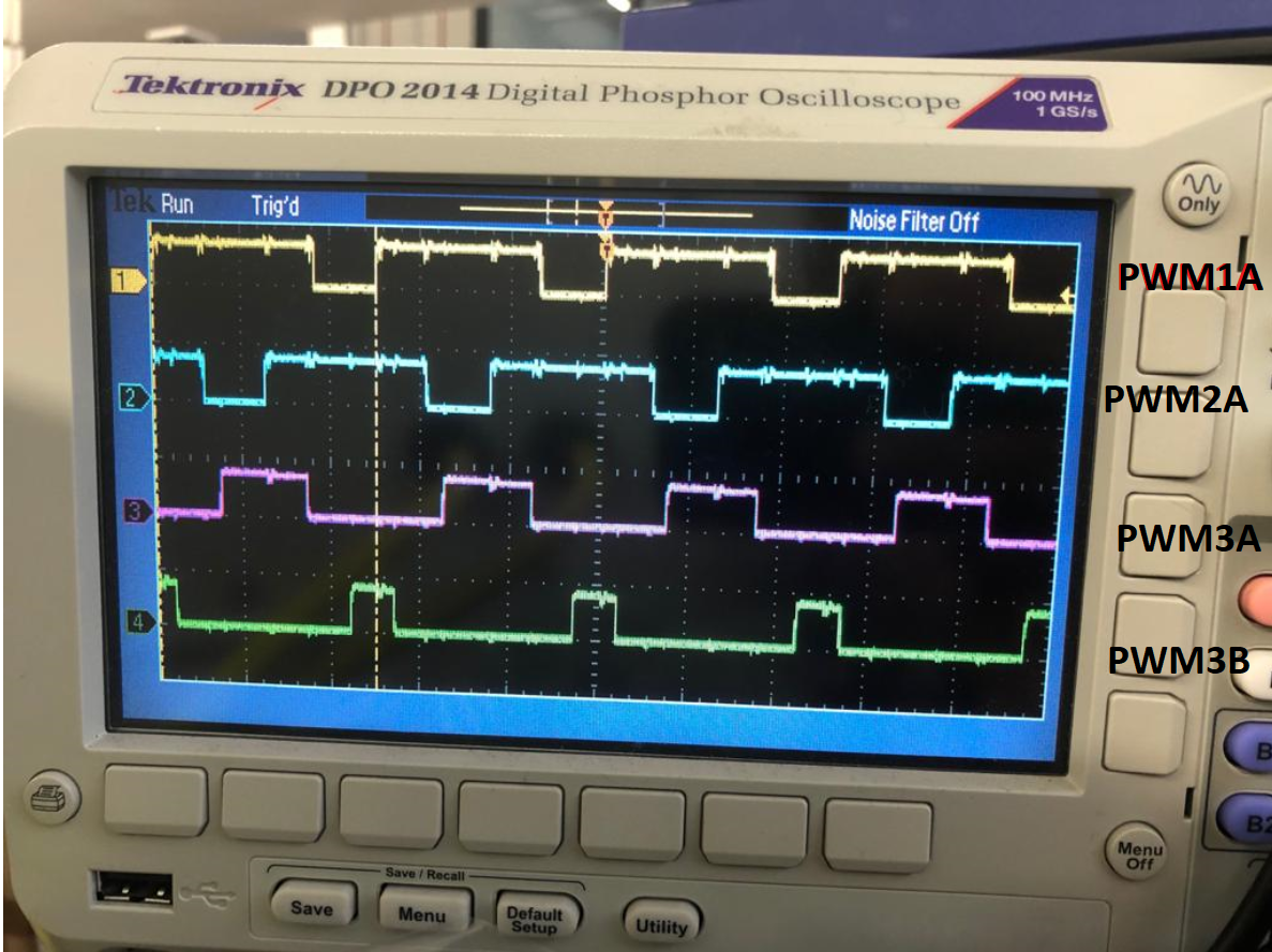
Hi,
I have two PWM signals, PWM1 and PWM2 which are generated using "/* Model initialize function */". I want to read the states of pins (GPIO0 for PWM1A & GPIO2 for PWM2A) and writing them back out in pins (GPIO4 as PWM3A and GPIO5 as PWM3B) without the need to initialise PWM3. I used different GPIO registers as can be shown in the code below but I am not exactly getting the same signals produced by GPIO0 and GPIO2. There is some delay in signals output from GPIO4 and GPIO5 and sometimes at specific duty cycles when I changed the values of the CAMP registers of PWM1 and PWM2, I don't get any output signals from pins GPIO4 and GPIO5. So please help me out?
#include "StackedTwoPhase.h"
#include "StackedTwoPhase_private.h"

/* Block signals (default storage) */
B_StackedTwoPhase_T StackedTwoPhase_B;

/* Real-time model */
RT_MODEL_StackedTwoPhase_T StackedTwoPhase_M_;
RT_MODEL_StackedTwoPhase_T *const StackedTwoPhase_M = &StackedTwoPhase_M_;

/* Model step function */
void StackedTwoPhase_step(void)
{
/* local block i/o variables */
real_T rtb_TMPRRD;


/* S-Function (c280xgpio_di): '<Root>/Digital Input' */
{

StackedTwoPhase_B.I1 = GpioDataRegs.GPADAT.bit.GPIO0;

}

/* S-Function (c280xgpio_di): '<Root>/Digital Input1' */
{

StackedTwoPhase_B.I2 = GpioDataRegs.GPADAT.bit.GPIO2;

}

/* MATLAB Function: '<Root>/MATLAB Function1' incorporates:
* Constant: '<Root>/Constant'
*/


/* End of MATLAB Function: '<Root>/MATLAB Function1' */

/* S-Function (c280xgpio_do): '<Root>/Digital Output' */
{

if (StackedTwoPhase_B.I1)

GpioDataRegs.GPASET.bit.GPIO4=1;

else

GpioDataRegs.GPACLEAR.bit.GPIO4=1;

}

/* S-Function (c280xgpio_do): '<Root>/Digital Output1' */
{

if (StackedTwoPhase_B.I2)

GpioDataRegs.GPASET.bit.GPIO5=1;

else

GpioDataRegs.GPACLEAR.bit.GPIO5=1;

}

/* Gain: '<Root>/TMPRRD' incorporates:
* Constant: '<Root>/Constant'
*/
rtb_TMPRRD = StackedTwoPhase_P.TMPRRD_Gain * StackedTwoPhase_P.Constant_Value;

/* S-Function (c2802xpwm): '<Root>/ePWM1' */

/*-- Update CMPA value for ePWM1 --*/
{
EPwm1Regs.CMPA.bit.CMPA = (uint16_T)(rtb_TMPRRD);
}

/* S-Function (c2802xpwm): '<Root>/ePWM2' incorporates:
* Constant: '<Root>/Phase_2'
*/
EPwm2Regs.TBPHS.bit.TBPHS = 499;

/*-- Update CMPA value for ePWM2 --*/
{
EPwm2Regs.CMPA.bit.CMPA = (uint16_T)(rtb_TMPRRD);
}
}

/* Model initialize function */
void StackedTwoPhase_initialize(void)
{
/* Registration code */


/* Start for S-Function (c280xgpio_do): '<Root>/Digital Output' */
EALLOW;
GpioCtrlRegs.GPADIR.bit.GPIO4 = 1;

EDIS;

/* Start for S-Function (c280xgpio_do): '<Root>/Digital Output1' */
EALLOW;
GpioCtrlRegs.GPADIR.bit.GPIO5 = 1;

EDIS;
/* Start for S-Function (c2802xpwm): '<Root>/ePWM1' */
EALLOW;
CpuSysRegs.PCLKCR2.bit.EPWM1 = 1;
CpuSysRegs.PCLKCR0.bit.TBCLKSYNC = 0;
EDIS;

/*** Initialize ePWM1 modules ***/
{
/* // Time Base Control Register
EPwm1Regs.TBCTL.bit.CTRMODE = 0; // Counter Mode
EPwm1Regs.TBCTL.bit.SYNCOSEL = 1; // Sync Output Select
EPwm1Regs.TBCTL.bit.PRDLD = 0; // Shadow select
EPwm1Regs.TBCTL.bit.PHSEN = 0; // Phase Load Enable
EPwm1Regs.TBCTL.bit.PHSDIR = 0; // Phase Direction Bit
EPwm1Regs.TBCTL.bit.HSPCLKDIV = 0; // High Speed TBCLK Pre-scaler
EPwm1Regs.TBCTL.bit.CLKDIV = 0; // Time Base Clock Pre-scaler
EPwm1Regs.TBCTL.bit.SWFSYNC = 0; // Software Force Sync Pulse
*/
EPwm1Regs.TBCTL.all = (EPwm1Regs.TBCTL.all & ~0x3FFF) | 0x10;

/*-- Setup Time-Base (TB) Submodule --*/
EPwm1Regs.TBPRD = 999; // Time Base Period Register

/* // Time-Base Phase Register
EPwm1Regs.TBPHS.bit.TBPHS = 0; // Phase offset register
*/
EPwm1Regs.TBPHS.all = (EPwm1Regs.TBPHS.all & ~0xFFFF0000) | 0x0;

// Time Base Counter Register
EPwm1Regs.TBCTR = 0x0000; /* Clear counter*/

/*-- Setup Counter_Compare (CC) Submodule --*/
/* // Counter Compare Control Register
EPwm1Regs.CMPCTL.bit.SHDWAMODE = 0; // Compare A Register Block Operating Mode
EPwm1Regs.CMPCTL.bit.SHDWBMODE = 0; // Compare B Register Block Operating Mode
EPwm1Regs.CMPCTL.bit.LOADAMODE = 0; // Active Compare A Load
EPwm1Regs.CMPCTL.bit.LOADBMODE = 0; // Active Compare B Load
*/
EPwm1Regs.CMPCTL.all = (EPwm1Regs.CMPCTL.all & ~0x5F) | 0x0;

/* EPwm1Regs.CMPCTL2.bit.SHDWCMODE = 0; // Compare C Register Block Operating Mode

EPwm1Regs.CMPCTL2.bit.SHDWDMODE = 0; // Compare D Register Block Operating Mode
*/
EPwm1Regs.CMPCTL2.all = (EPwm1Regs.CMPCTL2.all & ~0x50) | 0x0;
EPwm1Regs.CMPA.bit.CMPA = 0; // Counter Compare A Register
EPwm1Regs.CMPB.bit.CMPB = 0; // Counter Compare B Register
EPwm1Regs.CMPC = 0; // Counter Compare C Register
EPwm1Regs.CMPD = 0; // Counter Compare D Register

/*-- Setup Action-Qualifier (AQ) Submodule --*/
EPwm1Regs.AQCTLA.all = 33; // Action Qualifier Control Register For Output A
EPwm1Regs.AQCTLB.all = 33; // Action Qualifier Control Register For Output B

/* // Action Qualifier Software Force Register
EPwm1Regs.AQSFRC.bit.RLDCSF = 0; // Reload from Shadow Options
*/
EPwm1Regs.AQSFRC.all = (EPwm1Regs.AQSFRC.all & ~0xC0) | 0x0;

/* // Action Qualifier Continuous S/W Force Register
EPwm1Regs.AQCSFRC.bit.CSFA = 0; // Continuous Software Force on output A
EPwm1Regs.AQCSFRC.bit.CSFB = 0; // Continuous Software Force on output B
*/
EPwm1Regs.AQCSFRC.all = (EPwm1Regs.AQCSFRC.all & ~0xF) | 0x0;

/*-- Setup Dead-Band Generator (DB) Submodule --*/
/* // Dead-Band Generator Control Register
EPwm1Regs.DBCTL.bit.OUT_MODE = 3; // Dead Band Output Mode Control
EPwm1Regs.DBCTL.bit.IN_MODE = 0; // Dead Band Input Select Mode Control
EPwm1Regs.DBCTL.bit.POLSEL = 2; // Polarity Select Control
EPwm1Regs.DBCTL.bit.HALFCYCLE = 0; // Half Cycle Clocking Enable
*/
EPwm1Regs.DBCTL.all = (EPwm1Regs.DBCTL.all & ~0x803F) | 0xB;
EPwm1Regs.DBRED.bit.DBRED = 20; // Dead-Band Generator Rising Edge Delay Count Register
EPwm1Regs.DBFED.bit.DBFED = 20; // Dead-Band Generator Falling Edge Delay Count Register

/*-- Setup Event-Trigger (ET) Submodule --*/
/* // Event Trigger Selection and Pre-Scale Register
EPwm1Regs.ETSEL.bit.SOCAEN = 1; // Start of Conversion A Enable
EPwm1Regs.ETSEL.bit.SOCASELCMP = 0;
EPwm1Regs.ETSEL.bit.SOCASEL = 4 ; // Start of Conversion A Select
EPwm1Regs.ETPS.bit.SOCAPRD = 1; // EPWM1SOCA Period Select

EPwm1Regs.ETSEL.bit.SOCBEN = 0; // Start of Conversion B Enable

EPwm1Regs.ETSEL.bit.SOCBSELCMP = 0;
EPwm1Regs.ETSEL.bit.SOCBSEL = 1; // Start of Conversion A Select
EPwm1Regs.ETPS.bit.SOCBPRD = 1; // EPWM1SOCB Period Select
EPwm1Regs.ETSEL.bit.INTEN = 0; // EPWM1INTn Enable
EPwm1Regs.ETSEL.bit.INTSELCMP = 0;
EPwm1Regs.ETSEL.bit.INTSEL = 4; // Start of Conversion A Select

EPwm1Regs.ETPS.bit.INTPRD = 1; // EPWM1INTn Period Select
*/
EPwm1Regs.ETSEL.all = (EPwm1Regs.ETSEL.all & ~0xFF7F) | 0x1C04;
EPwm1Regs.ETPS.all = (EPwm1Regs.ETPS.all & ~0x3303) | 0x1101;

/*-- Setup PWM-Chopper (PC) Submodule --*/
/* // PWM Chopper Control Register
EPwm1Regs.PCCTL.bit.CHPEN = 0; // PWM chopping enable
EPwm1Regs.PCCTL.bit.CHPFREQ = 0; // Chopping clock frequency
EPwm1Regs.PCCTL.bit.OSHTWTH = 0; // One-shot pulse width
EPwm1Regs.PCCTL.bit.CHPDUTY = 0; // Chopping clock Duty cycle
*/
EPwm1Regs.PCCTL.all = (EPwm1Regs.PCCTL.all & ~0x7FF) | 0x0;

/*-- Set up Trip-Zone (TZ) Submodule --*/
EALLOW;
EPwm1Regs.TZSEL.all = 0; // Trip Zone Select Register

/* // Trip Zone Control Register
EPwm1Regs.TZCTL.bit.TZA = 3; // TZ1 to TZ6 Trip Action On EPWM1A
EPwm1Regs.TZCTL.bit.TZB = 3; // TZ1 to TZ6 Trip Action On EPWM1B
EPwm1Regs.TZCTL.bit.DCAEVT1 = 3; // EPWM1A action on DCAEVT1
EPwm1Regs.TZCTL.bit.DCAEVT2 = 3; // EPWM1A action on DCAEVT2
EPwm1Regs.TZCTL.bit.DCBEVT1 = 3; // EPWM1B action on DCBEVT1
EPwm1Regs.TZCTL.bit.DCBEVT2 = 3; // EPWM1B action on DCBEVT2
*/
EPwm1Regs.TZCTL.all = (EPwm1Regs.TZCTL.all & ~0xFFF) | 0xFFF;

/* // Trip Zone Enable Interrupt Register
EPwm1Regs.TZEINT.bit.OST = 0; // Trip Zones One Shot Int Enable
EPwm1Regs.TZEINT.bit.CBC = 0; // Trip Zones Cycle By Cycle Int Enable
EPwm1Regs.TZEINT.bit.DCAEVT1 = 0; // Digital Compare A Event 1 Int Enable
EPwm1Regs.TZEINT.bit.DCAEVT2 = 0; // Digital Compare A Event 2 Int Enable
EPwm1Regs.TZEINT.bit.DCBEVT1 = 0; // Digital Compare B Event 1 Int Enable
EPwm1Regs.TZEINT.bit.DCBEVT2 = 0; // Digital Compare B Event 2 Int Enable
*/
EPwm1Regs.TZEINT.all = (EPwm1Regs.TZEINT.all & ~0x7E) | 0x0;

/* // Digital Compare A Control Register
EPwm1Regs.DCACTL.bit.EVT1SYNCE = 0; // DCAEVT1 SYNC Enable
EPwm1Regs.DCACTL.bit.EVT1SOCE = 1; // DCAEVT1 SOC Enable
EPwm1Regs.DCACTL.bit.EVT1FRCSYNCSEL = 0; // DCAEVT1 Force Sync Signal
EPwm1Regs.DCACTL.bit.EVT1SRCSEL = 0; // DCAEVT1 Source Signal
EPwm1Regs.DCACTL.bit.EVT2FRCSYNCSEL = 0; // DCAEVT2 Force Sync Signal
EPwm1Regs.DCACTL.bit.EVT2SRCSEL = 0; // DCAEVT2 Source Signal
*/
EPwm1Regs.DCACTL.all = (EPwm1Regs.DCACTL.all & ~0x30F) | 0x4;

/* // Digital Compare B Control Register
EPwm1Regs.DCBCTL.bit.EVT1SYNCE = 0; // DCBEVT1 SYNC Enable
EPwm1Regs.DCBCTL.bit.EVT1SOCE = 0; // DCBEVT1 SOC Enable
EPwm1Regs.DCBCTL.bit.EVT1FRCSYNCSEL = 0; // DCBEVT1 Force Sync Signal
EPwm1Regs.DCBCTL.bit.EVT1SRCSEL = 0; // DCBEVT1 Source Signal
EPwm1Regs.DCBCTL.bit.EVT2FRCSYNCSEL = 0; // DCBEVT2 Force Sync Signal
EPwm1Regs.DCBCTL.bit.EVT2SRCSEL = 0; // DCBEVT2 Source Signal
*/
EPwm1Regs.DCBCTL.all = (EPwm1Regs.DCBCTL.all & ~0x30F) | 0x0;

/* // Digital Compare Trip Select Register
EPwm1Regs.DCTRIPSEL.bit.DCAHCOMPSEL = 0; // Digital Compare A High COMP Input Select

EPwm1Regs.DCTRIPSEL.bit.DCALCOMPSEL = 1; // Digital Compare A Low COMP Input Select
EPwm1Regs.DCTRIPSEL.bit.DCBHCOMPSEL = 0; // Digital Compare B High COMP Input Select
EPwm1Regs.DCTRIPSEL.bit.DCBLCOMPSEL = 1; // Digital Compare B Low COMP Input Select


*/
EPwm1Regs.DCTRIPSEL.all = (EPwm1Regs.DCTRIPSEL.all & ~ 0xFFFF) | 0x1010;

/* // Trip Zone Digital Comparator Select Register
EPwm1Regs.TZDCSEL.bit.DCAEVT1 = 0; // Digital Compare Output A Event 1
EPwm1Regs.TZDCSEL.bit.DCAEVT2 = 0; // Digital Compare Output A Event 2
EPwm1Regs.TZDCSEL.bit.DCBEVT1 = 0; // Digital Compare Output B Event 1
EPwm1Regs.TZDCSEL.bit.DCBEVT2 = 0; // Digital Compare Output B Event 2
*/
EPwm1Regs.TZDCSEL.all = (EPwm1Regs.TZDCSEL.all & ~0xFFF) | 0x0;

/* // Digital Compare Filter Control Register
EPwm1Regs.DCFCTL.bit.BLANKE = 0; // Blanking Enable/Disable
EPwm1Regs.DCFCTL.bit.PULSESEL = 1; // Pulse Select for Blanking & Capture Alignment
EPwm1Regs.DCFCTL.bit.BLANKINV = 0; // Blanking Window Inversion
EPwm1Regs.DCFCTL.bit.SRCSEL = 0; // Filter Block Signal Source Select
*/
EPwm1Regs.DCFCTL.all = (EPwm1Regs.DCFCTL.all & ~0x3F) | 0x10;
EPwm1Regs.DCFOFFSET = 0; // Digital Compare Filter Offset Register
EPwm1Regs.DCFWINDOW = 0; // Digital Compare Filter Window Register

/* // Digital Compare Capture Control Register
EPwm1Regs.DCCAPCTL.bit.CAPE = 0; // Counter Capture Enable
*/
EPwm1Regs.DCCAPCTL.all = (EPwm1Regs.DCCAPCTL.all & ~0x1) | 0x0;

/* // HRPWM Configuration Register
EPwm1Regs.HRCNFG.bit.SWAPAB = 0; // Swap EPWMA and EPWMB Outputs Bit
EPwm1Regs.HRCNFG.bit.SELOUTB = 0; // EPWMB Output Selection Bit
*/
EPwm1Regs.HRCNFG.all = (EPwm1Regs.HRCNFG.all & ~0xA0) | 0x0;

/* Update the Link Registers with the link value for all the Compare values and TBPRD */
/* No error is thrown if the ePWM register exists in the model or not */
EPwm1Regs.EPWMXLINK.bit.TBPRDLINK = 0;
EPwm1Regs.EPWMXLINK.bit.CMPALINK = 0;
EPwm1Regs.EPWMXLINK.bit.CMPBLINK = 0;
EPwm1Regs.EPWMXLINK.bit.CMPCLINK = 0;
EPwm1Regs.EPWMXLINK.bit.CMPDLINK = 0;
EDIS;
EALLOW;
CpuSysRegs.PCLKCR0.bit.TBCLKSYNC = 1;
EDIS;
}

/* Start for S-Function (c2802xpwm): '<Root>/ePWM2' incorporates:
* Constant: '<Root>/Phase_2'
*/
EALLOW;
CpuSysRegs.PCLKCR2.bit.EPWM2 = 1;
CpuSysRegs.PCLKCR0.bit.TBCLKSYNC = 0;
EDIS;

/*** Initialize ePWM2 modules ***/
{
/* // Time Base Control Register
EPwm2Regs.TBCTL.bit.CTRMODE = 0; // Counter Mode
EPwm2Regs.TBCTL.bit.SYNCOSEL = 0; // Sync Output Select
EPwm2Regs.TBCTL.bit.PRDLD = 0; // Shadow select
EPwm2Regs.TBCTL.bit.PHSEN = 1; // Phase Load Enable
EPwm2Regs.TBCTL.bit.PHSDIR = 0; // Phase Direction Bit
EPwm2Regs.TBCTL.bit.HSPCLKDIV = 0; // High Speed TBCLK Pre-scaler
EPwm2Regs.TBCTL.bit.CLKDIV = 0; // Time Base Clock Pre-scaler
EPwm2Regs.TBCTL.bit.SWFSYNC = 0; // Software Force Sync Pulse
*/
EPwm2Regs.TBCTL.all = (EPwm2Regs.TBCTL.all & ~0x3FFF) | 0x4;

/*-- Setup Time-Base (TB) Submodule --*/
EPwm2Regs.TBPRD = 999; // Time Base Period Register

/* // Time-Base Phase Register
EPwm2Regs.TBPHS.bit.TBPHS = 0; // Phase offset register
*/
EPwm2Regs.TBPHS.all = (EPwm2Regs.TBPHS.all & ~0xFFFF0000) | 0x0;

// Time Base Counter Register
EPwm2Regs.TBCTR = 0x0000; /* Clear counter*/

/*-- Setup Counter_Compare (CC) Submodule --*/
/* // Counter Compare Control Register
EPwm2Regs.CMPCTL.bit.SHDWAMODE = 0; // Compare A Register Block Operating Mode
EPwm2Regs.CMPCTL.bit.SHDWBMODE = 0; // Compare B Register Block Operating Mode
EPwm2Regs.CMPCTL.bit.LOADAMODE = 0; // Active Compare A Load
EPwm2Regs.CMPCTL.bit.LOADBMODE = 0; // Active Compare B Load
*/
EPwm2Regs.CMPCTL.all = (EPwm2Regs.CMPCTL.all & ~0x5F) | 0x0;

/* EPwm2Regs.CMPCTL2.bit.SHDWCMODE = 0; // Compare C Register Block Operating Mode

EPwm2Regs.CMPCTL2.bit.SHDWDMODE = 0; // Compare D Register Block Operating Mode
*/
EPwm2Regs.CMPCTL2.all = (EPwm2Regs.CMPCTL2.all & ~0x50) | 0x0;
EPwm2Regs.CMPA.bit.CMPA = 0; // Counter Compare A Register
EPwm2Regs.CMPB.bit.CMPB = 0; // Counter Compare B Register
EPwm2Regs.CMPC = 0; // Counter Compare C Register
EPwm2Regs.CMPD = 0; // Counter Compare D Register

/*-- Setup Action-Qualifier (AQ) Submodule --*/
EPwm2Regs.AQCTLA.all = 97; // Action Qualifier Control Register For Output A
EPwm2Regs.AQCTLB.all = 33; // Action Qualifier Control Register For Output B

/* // Action Qualifier Software Force Register
EPwm2Regs.AQSFRC.bit.RLDCSF = 0; // Reload from Shadow Options
*/
EPwm2Regs.AQSFRC.all = (EPwm2Regs.AQSFRC.all & ~0xC0) | 0x0;

/* // Action Qualifier Continuous S/W Force Register
EPwm2Regs.AQCSFRC.bit.CSFA = 0; // Continuous Software Force on output A
EPwm2Regs.AQCSFRC.bit.CSFB = 0; // Continuous Software Force on output B
*/
EPwm2Regs.AQCSFRC.all = (EPwm2Regs.AQCSFRC.all & ~0xF) | 0x0;

/*-- Setup Dead-Band Generator (DB) Submodule --*/
/* // Dead-Band Generator Control Register
EPwm2Regs.DBCTL.bit.OUT_MODE = 3; // Dead Band Output Mode Control
EPwm2Regs.DBCTL.bit.IN_MODE = 0; // Dead Band Input Select Mode Control
EPwm2Regs.DBCTL.bit.POLSEL = 2; // Polarity Select Control
EPwm2Regs.DBCTL.bit.HALFCYCLE = 0; // Half Cycle Clocking Enable
*/
EPwm2Regs.DBCTL.all = (EPwm2Regs.DBCTL.all & ~0x803F) | 0xB;
EPwm2Regs.DBRED.bit.DBRED = 20; // Dead-Band Generator Rising Edge Delay Count Register
EPwm2Regs.DBFED.bit.DBFED = 20; // Dead-Band Generator Falling Edge Delay Count Register

/*-- Setup Event-Trigger (ET) Submodule --*/
/* // Event Trigger Selection and Pre-Scale Register
EPwm2Regs.ETSEL.bit.SOCAEN = 1; // Start of Conversion A Enable
EPwm2Regs.ETSEL.bit.SOCASELCMP = 0;
EPwm2Regs.ETSEL.bit.SOCASEL = 4 ; // Start of Conversion A Select
EPwm2Regs.ETPS.bit.SOCAPRD = 1; // EPWM2SOCA Period Select

EPwm2Regs.ETSEL.bit.SOCBEN = 0; // Start of Conversion B Enable

EPwm2Regs.ETSEL.bit.SOCBSELCMP = 0;
EPwm2Regs.ETSEL.bit.SOCBSEL = 1; // Start of Conversion A Select
EPwm2Regs.ETPS.bit.SOCBPRD = 1; // EPWM2SOCB Period Select
EPwm2Regs.ETSEL.bit.INTEN = 0; // EPWM2INTn Enable
EPwm2Regs.ETSEL.bit.INTSELCMP = 0;
EPwm2Regs.ETSEL.bit.INTSEL = 4; // Start of Conversion A Select

EPwm2Regs.ETPS.bit.INTPRD = 1; // EPWM2INTn Period Select
*/
EPwm2Regs.ETSEL.all = (EPwm2Regs.ETSEL.all & ~0xFF7F) | 0x1C04;
EPwm2Regs.ETPS.all = (EPwm2Regs.ETPS.all & ~0x3303) | 0x1101;

/*-- Setup PWM-Chopper (PC) Submodule --*/
/* // PWM Chopper Control Register
EPwm2Regs.PCCTL.bit.CHPEN = 0; // PWM chopping enable
EPwm2Regs.PCCTL.bit.CHPFREQ = 0; // Chopping clock frequency
EPwm2Regs.PCCTL.bit.OSHTWTH = 0; // One-shot pulse width
EPwm2Regs.PCCTL.bit.CHPDUTY = 0; // Chopping clock Duty cycle
*/
EPwm2Regs.PCCTL.all = (EPwm2Regs.PCCTL.all & ~0x7FF) | 0x0;

/*-- Set up Trip-Zone (TZ) Submodule --*/
EALLOW;
EPwm2Regs.TZSEL.all = 0; // Trip Zone Select Register

/* // Trip Zone Control Register
EPwm2Regs.TZCTL.bit.TZA = 3; // TZ1 to TZ6 Trip Action On EPWM2A
EPwm2Regs.TZCTL.bit.TZB = 3; // TZ1 to TZ6 Trip Action On EPWM2B
EPwm2Regs.TZCTL.bit.DCAEVT1 = 3; // EPWM2A action on DCAEVT1
EPwm2Regs.TZCTL.bit.DCAEVT2 = 3; // EPWM2A action on DCAEVT2
EPwm2Regs.TZCTL.bit.DCBEVT1 = 3; // EPWM2B action on DCBEVT1
EPwm2Regs.TZCTL.bit.DCBEVT2 = 3; // EPWM2B action on DCBEVT2
*/
EPwm2Regs.TZCTL.all = (EPwm2Regs.TZCTL.all & ~0xFFF) | 0xFFF;

/* // Trip Zone Enable Interrupt Register
EPwm2Regs.TZEINT.bit.OST = 0; // Trip Zones One Shot Int Enable
EPwm2Regs.TZEINT.bit.CBC = 0; // Trip Zones Cycle By Cycle Int Enable
EPwm2Regs.TZEINT.bit.DCAEVT1 = 0; // Digital Compare A Event 1 Int Enable
EPwm2Regs.TZEINT.bit.DCAEVT2 = 0; // Digital Compare A Event 2 Int Enable
EPwm2Regs.TZEINT.bit.DCBEVT1 = 0; // Digital Compare B Event 1 Int Enable
EPwm2Regs.TZEINT.bit.DCBEVT2 = 0; // Digital Compare B Event 2 Int Enable
*/
EPwm2Regs.TZEINT.all = (EPwm2Regs.TZEINT.all & ~0x7E) | 0x0;

/* // Digital Compare A Control Register
EPwm2Regs.DCACTL.bit.EVT1SYNCE = 0; // DCAEVT1 SYNC Enable
EPwm2Regs.DCACTL.bit.EVT1SOCE = 1; // DCAEVT1 SOC Enable
EPwm2Regs.DCACTL.bit.EVT1FRCSYNCSEL = 0; // DCAEVT1 Force Sync Signal
EPwm2Regs.DCACTL.bit.EVT1SRCSEL = 0; // DCAEVT1 Source Signal
EPwm2Regs.DCACTL.bit.EVT2FRCSYNCSEL = 0; // DCAEVT2 Force Sync Signal
EPwm2Regs.DCACTL.bit.EVT2SRCSEL = 0; // DCAEVT2 Source Signal
*/
EPwm2Regs.DCACTL.all = (EPwm2Regs.DCACTL.all & ~0x30F) | 0x4;

/* // Digital Compare B Control Register
EPwm2Regs.DCBCTL.bit.EVT1SYNCE = 0; // DCBEVT1 SYNC Enable
EPwm2Regs.DCBCTL.bit.EVT1SOCE = 0; // DCBEVT1 SOC Enable
EPwm2Regs.DCBCTL.bit.EVT1FRCSYNCSEL = 0; // DCBEVT1 Force Sync Signal
EPwm2Regs.DCBCTL.bit.EVT1SRCSEL = 0; // DCBEVT1 Source Signal
EPwm2Regs.DCBCTL.bit.EVT2FRCSYNCSEL = 0; // DCBEVT2 Force Sync Signal
EPwm2Regs.DCBCTL.bit.EVT2SRCSEL = 0; // DCBEVT2 Source Signal
*/
EPwm2Regs.DCBCTL.all = (EPwm2Regs.DCBCTL.all & ~0x30F) | 0x0;

/* // Digital Compare Trip Select Register
EPwm2Regs.DCTRIPSEL.bit.DCAHCOMPSEL = 0; // Digital Compare A High COMP Input Select

EPwm2Regs.DCTRIPSEL.bit.DCALCOMPSEL = 1; // Digital Compare A Low COMP Input Select
EPwm2Regs.DCTRIPSEL.bit.DCBHCOMPSEL = 0; // Digital Compare B High COMP Input Select
EPwm2Regs.DCTRIPSEL.bit.DCBLCOMPSEL = 1; // Digital Compare B Low COMP Input Select


*/
EPwm2Regs.DCTRIPSEL.all = (EPwm2Regs.DCTRIPSEL.all & ~ 0xFFFF) | 0x1010;

/* // Trip Zone Digital Comparator Select Register
EPwm2Regs.TZDCSEL.bit.DCAEVT1 = 0; // Digital Compare Output A Event 1
EPwm2Regs.TZDCSEL.bit.DCAEVT2 = 0; // Digital Compare Output A Event 2
EPwm2Regs.TZDCSEL.bit.DCBEVT1 = 0; // Digital Compare Output B Event 1
EPwm2Regs.TZDCSEL.bit.DCBEVT2 = 0; // Digital Compare Output B Event 2
*/
EPwm2Regs.TZDCSEL.all = (EPwm2Regs.TZDCSEL.all & ~0xFFF) | 0x0;

/* // Digital Compare Filter Control Register
EPwm2Regs.DCFCTL.bit.BLANKE = 0; // Blanking Enable/Disable
EPwm2Regs.DCFCTL.bit.PULSESEL = 1; // Pulse Select for Blanking & Capture Alignment
EPwm2Regs.DCFCTL.bit.BLANKINV = 0; // Blanking Window Inversion
EPwm2Regs.DCFCTL.bit.SRCSEL = 0; // Filter Block Signal Source Select
*/
EPwm2Regs.DCFCTL.all = (EPwm2Regs.DCFCTL.all & ~0x3F) | 0x10;
EPwm2Regs.DCFOFFSET = 0; // Digital Compare Filter Offset Register
EPwm2Regs.DCFWINDOW = 0; // Digital Compare Filter Window Register

/* // Digital Compare Capture Control Register
EPwm2Regs.DCCAPCTL.bit.CAPE = 0; // Counter Capture Enable
*/
EPwm2Regs.DCCAPCTL.all = (EPwm2Regs.DCCAPCTL.all & ~0x1) | 0x0;

/* // HRPWM Configuration Register
EPwm2Regs.HRCNFG.bit.SWAPAB = 0; // Swap EPWMA and EPWMB Outputs Bit
EPwm2Regs.HRCNFG.bit.SELOUTB = 0; // EPWMB Output Selection Bit
*/
EPwm2Regs.HRCNFG.all = (EPwm2Regs.HRCNFG.all & ~0xA0) | 0x0;

/* Update the Link Registers with the link value for all the Compare values and TBPRD */
/* No error is thrown if the ePWM register exists in the model or not */
EPwm2Regs.EPWMXLINK.bit.TBPRDLINK = 1;
EPwm2Regs.EPWMXLINK.bit.CMPALINK = 1;
EPwm2Regs.EPWMXLINK.bit.CMPBLINK = 1;
EPwm2Regs.EPWMXLINK.bit.CMPCLINK = 1;
EPwm2Regs.EPWMXLINK.bit.CMPDLINK = 1;
EDIS;
EALLOW;
CpuSysRegs.PCLKCR0.bit.TBCLKSYNC = 1;
EDIS;
}
}

/* Model terminate function */
void StackedTwoPhase_terminate(void)
{
/* (no terminate code required) */
}

/*
* File trailer for generated code.
*
* [EOF]
*/