Other Parts Discussed in Thread: C2000WARE
Hello,
My customer is using TMS320F28379D and having trouble with PWM output.
They are using CLA for updating EPWM_REGS shadow registers, ISR is triggered by ADC conversion complete.
ADC sampling period: 1us
PWM cycle : 0.2us
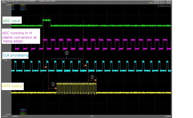
In the 1st screenshot above, there are 1us latency after CLA processing completion to PWM update (see ①)
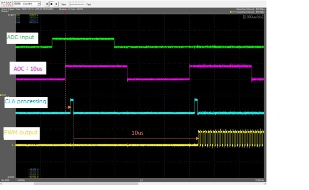
When changing the ADC sampling period from 1us to 10us, the latency ① also becomes 10us. Please see the 2nd screenshot.
How can we reduce the latency?
Also, it looks like CLA processing results in period ② in the 1st screenshot are not reflected to the PWM output.
Are there any limitation?
Here are EPWM register settings.
==================
EPwm1Regs.TBCTL.all = (EPwm1Regs.TBCTL.all & ~0x3FFF) | 0x38;
EPwm1Regs.TBPRD = 19; // Time Base Period Register
EPwm1Regs.TBPHS.all = (EPwm1Regs.TBPHS.all & ~0xFFFF0000) | 0x0;
EPwm1Regs.TBCTR = 0x0000; /* Clear counter*/
EPwm1Regs.CMPCTL.all = (EPwm1Regs.CMPCTL.all & ~0x5F) | 0x0;
EPwm1Regs.CMPCTL2.all = (EPwm1Regs.CMPCTL2.all & ~0x50) | 0x0;
EPwm1Regs.CMPA.bit.CMPA = 10; // Counter Compare A Register
EPwm1Regs.CMPB.bit.CMPB = 32000; // Counter Compare B Register
EPwm1Regs.CMPC = 32000; // Counter Compare C Register
EPwm1Regs.CMPD = 32000; // Counter Compare D Register
EPwm1Regs.AQCTLA.all = 146; // Action Qualifier Control Register For Output A
EPwm1Regs.AQCTLB.all = 2310; // Action Qualifier Control Register For Output B
EPwm1Regs.AQSFRC.all = (EPwm1Regs.AQSFRC.all & ~0xC0) | 0x0;
EPwm1Regs.AQCSFRC.all = (EPwm1Regs.AQCSFRC.all & ~0xF) | 0x0;
EPwm1Regs.DBCTL.all = (EPwm1Regs.DBCTL.all & ~0x803F) | 0x0;
EPwm1Regs.DBRED.bit.DBRED = 0; // Dead-Band Generator Rising Edge Delay Count Register
EPwm1Regs.DBFED.bit.DBFED = 0; // Dead-Band Generator Falling Edge Delay Count Register
EPwm1Regs.ETSEL.all = (EPwm1Regs.ETSEL.all & ~0xFF7F) | 0x1001;
EPwm1Regs.ETPS.all = (EPwm1Regs.ETPS.all & ~0x3303) | 0x1101;
EPwm1Regs.PCCTL.all = (EPwm1Regs.PCCTL.all & ~0x7FF) | 0x0;
EPwm1Regs.TZSEL.all = 0; // Trip Zone Select Register
EPwm1Regs.TZCTL.all = (EPwm1Regs.TZCTL.all & ~0xFFF) | 0xFFF;
EPwm1Regs.TZEINT.all = (EPwm1Regs.TZEINT.all & ~0x7E) | 0x0;
EPwm1Regs.DCACTL.all = (EPwm1Regs.DCACTL.all & ~0x30F) | 0x4;
EPwm1Regs.DCBCTL.all = (EPwm1Regs.DCBCTL.all & ~0x30F) | 0x0;
EPwm1Regs.DCTRIPSEL.all = (EPwm1Regs.DCTRIPSEL.all & ~ 0xFFFF) | 0x1010;
EPwm1Regs.TZDCSEL.all = (EPwm1Regs.TZDCSEL.all & ~0xFFF) | 0x0;
EPwm1Regs.DCFCTL.all = (EPwm1Regs.DCFCTL.all & ~0x3F) | 0x10;
EPwm1Regs.DCFOFFSET = 0; // Digital Compare Filter Offset Register
EPwm1Regs.DCFWINDOW = 0; // Digital Compare Filter Window Register
EPwm1Regs.DCCAPCTL.all = (EPwm1Regs.DCCAPCTL.all & ~0x1) | 0x0;
EPwm1Regs.HRCNFG.all = (EPwm1Regs.HRCNFG.all & ~0xA0) | 0x0;
EPwm1Regs.EPWMXLINK.bit.TBPRDLINK = 0;
EPwm1Regs.EPWMXLINK.bit.CMPALINK = 0;
EPwm1Regs.EPWMXLINK.bit.CMPBLINK = 0;
EPwm1Regs.EPWMXLINK.bit.CMPCLINK = 0;
EPwm1Regs.EPWMXLINK.bit.CMPDLINK = 0;
==================
Thanks & Regards,
-Shibata


