This thread has been locked.

If you have a related question, please click the "Ask a related question" button in the top right corner. The newly created question will be automatically linked to this question.

LAUNCHXL-F28069M: DMA configuration issue, Each burst transfer is not waiting for the Peripheral trigger when ONESHOT is disabled

Part Number: LAUNCHXL-F28069M

HI Team, 

We are using the DMA to generate the required number of PWM cycles and have issue with ONESHOT, When ONESHOT  is disabled its not waiting for the event so unable to count the number of PWM cycles. 


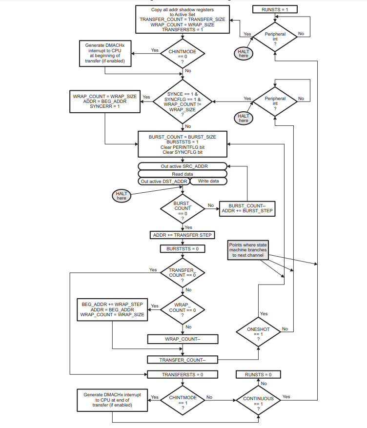
  1. We need to start the PWM on the ECAP interrupt, As ECAP cannot trigger the DMA, First we are triggering DMA with Software force bit is set (DmaRegs.CH1.CONTROL.bit.PERINTFRC = 1).
  • Here only one word (1 Burst of length 1 word ) will be transferred.
  • DMA transfer is completed and DMA interrupt is generated as shown in the diagram below. (DMA interrupt is generated at the end of the transfer).


  1. In the DMA_ISR, Initialize the DMA to trigger from the EPWM2SOCA on every CTR = PRD and start the transfer for 92 word (Burst length is 1 word, Total 92 transfer).

  • The ONESHOT bit (DmaRegs.CH1.MODE.bit.ONESHOT = 0) is not set so DMA should wait for Peripheral trigger (From PWM2 ADCSOC when CTR = PRD) after each transfer.


As you see in the diagram, After first DMA Interrupt(DMA_INT1) one word is getting transferred and after 2nd interrupt (DMA_INT2) remaining 92 words are transferred but the transfer is not happening on every PWM cycle, All 92 words are transferred on single PWM event, Seems it’s not waiting for trigger after each transfer. 

Please let me know if you need more details, Please test ONESHOT bit at your end and confirm. 

Thanks, 

Ajay 

  • Hi Team, 

    Please find the below code for your reference.


    In the ECAP ISR, DMA is configured, DMA_Transfer_Done flag is set in the DMA interrupt.

    ECAP ISR :
    {
    DMA_Transfer_Done = 0;
    DMACH1ConfigFRC(); //DMA config for SW FRC triggered 1 word transfer 
     
    while (!DMA_Transfer_Done);
     
    DMA_Transfer_Done = 0;
    DMACH1ConfigSOC(); //DMA config for SOC triggered 92 words transfer. 
    }
     
     
    DMA ISR : 
    __interrupt
    void Tx_DINTCH1_ISR(void)  // DMA INT7.1
    {
        DEBUG7_TOGGLE;
        DMA_Transfer_Done = 1;
        // Clear any spurious flags:
        EALLOW;
        DmaRegs.CH1.CONTROL.bit.PERINTCLR = 1;          // Clear any spurious interrupt flags
        DmaRegs.CH1.CONTROL.bit.ERRCLR = 1;             // Clear any spurious sync error flags
        EDIS;
        PieCtrlRegs.PIEACK.bit.ACK7 = 1;             // Clear PIEIFR bit
    }
     
     
    void DMACH1ConfigFRC(void)
    {
        EALLOW;
     
        // Set up MODE Register:
        DmaRegs.CH1.MODE.bit.PERINTSEL = 0;            // None, Force interrupt is used
        DmaRegs.CH1.MODE.bit.PERINTE = 1;               // Peripheral interrupt enabled
        DmaRegs.CH1.MODE.bit.ONESHOT = 1;               // burst transfers occur without additional event triggers after the first event trigger
        DmaRegs.CH1.MODE.bit.CONTINUOUS = 0;            // stop after each transfer
        DmaRegs.CH1.MODE.bit.DATASIZE = 0;              // 16-bit data size transfers
        DmaRegs.CH1.MODE.bit.CHINTMODE = 1;             // Generate interrupt at the end of transfer
        DmaRegs.CH1.MODE.bit.CHINTE = 1;                // Channel Interrupt to CPU enabled
     
        // Set up BURST registers:
        DmaRegs.CH1.BURST_SIZE.all = 0;                 // Number (N-1) of 16-bit words transferred in a burst
        DmaRegs.CH1.SRC_BURST_STEP = 0;                 // Add 1 to address
        DmaRegs.CH1.DST_BURST_STEP = 0;//1;//0;                 // Destination is same
     
        // Set up TRANSFER registers:
        DmaRegs.CH1.TRANSFER_SIZE = 0;//4499;                  // Bursts (N-1) per transfer
        DmaRegs.CH1.SRC_TRANSFER_STEP = 0;//0x001F;              // 1 transfer = 32 words
        DmaRegs.CH1.DST_TRANSFER_STEP = 0;//1;//0;                  // Destination is same
     
        // Set up WRAP registers:
        DmaRegs.CH1.SRC_WRAP_SIZE = 0xFFFF;             // No source wrap-around
        DmaRegs.CH1.DST_WRAP_SIZE = 0xFFFF;             // No destination wrap-around
        DmaRegs.CH1.SRC_WRAP_STEP = 0;
        DmaRegs.CH1.DST_WRAP_STEP = 0;
     
        // Set up SOURCE address:
        DmaRegs.CH1.SRC_BEG_ADDR_SHADOW = (Uint32) &TxCMP_58000[0];
        DmaRegs.CH1.SRC_ADDR_SHADOW = (Uint32) &TxCMP_58000[0];// Point to period table
     
        DmaRegs.CH1.DST_BEG_ADDR_SHADOW = (Uint32) &EPwm2Regs.CMPA.half.CMPA;
        DmaRegs.CH1.DST_ADDR_SHADOW = (Uint32) &EPwm2Regs.CMPA.half.CMPA;   // Point to ePWM1 TBPRD register remapped for DMA
                                                                    //   need to make sure .cmd file has ePWMs remapped
        // Clear any spurious flags:
        DmaRegs.CH1.CONTROL.bit.PERINTCLR = 1;          // Clear any spurious interrupt flags
     
        //start the DMA transfer
        DmaRegs.CH1.CONTROL.bit.RUN = 1;
        DmaRegs.CH1.CONTROL.bit.PERINTFRC = 1;
     
        PieCtrlRegs.PIEIER7.bit.INTx1 = 1;    // Enable DMA CH1 interrupt in PIE
        EDIS;
     
        IER |= M_INT7;                      // Enable INT7 in IER to enable PIE group 7
        EINT;                               // Enable Global interrupt INTM
        ERTM;                               // Enable Global realtime interrupt DBGM
    }
     
    void DMACH1ConfigSOC(void)
    {
        EALLOW;
     
        // Set up MODE Register:
        DmaRegs.CH1.MODE.bit.PERINTSEL = 18;            // None, Force interrupt is used
        DmaRegs.CH1.MODE.bit.PERINTE = 1;               // Peripheral interrupt enabled
        DmaRegs.CH1.MODE.bit.ONESHOT = 0;               // burst transfers occur with additional event triggers after the first event trigger
        DmaRegs.CH1.MODE.bit.CONTINUOUS = 0;            // Do not stop after each transfer
        DmaRegs.CH1.MODE.bit.DATASIZE = 0;              // 16-bit data size transfers
        DmaRegs.CH1.MODE.bit.CHINTMODE = 1;             // Generate interrupt at the end of transfer
        DmaRegs.CH1.MODE.bit.CHINTE = 1;                // Channel Interrupt to CPU enabled
     
        // Set up BURST registers:
        DmaRegs.CH1.BURST_SIZE.all = 0;                 // Number (N-1) of 16-bit words transferred in a burst
        DmaRegs.CH1.SRC_BURST_STEP = 0;                 // Add 1 to address
        DmaRegs.CH1.DST_BURST_STEP = 0;//1;//0;                 // Destination is same
     
        // Set up TRANSFER registers:
        DmaRegs.CH1.TRANSFER_SIZE = 91;//4499;                  // Bursts (N-1) per transfer
        DmaRegs.CH1.SRC_TRANSFER_STEP = 1;//0x001F;              // 1 transfer = 32 words
        DmaRegs.CH1.DST_TRANSFER_STEP = 0;//1;//0;                  // Destination is same
     
        // Set up WRAP registers:
        DmaRegs.CH1.SRC_WRAP_SIZE = 0xFFFF;             // No source wrap-around
        DmaRegs.CH1.DST_WRAP_SIZE = 0xFFFF;             // No destination wrap-around
        DmaRegs.CH1.SRC_WRAP_STEP = 0;
        DmaRegs.CH1.DST_WRAP_STEP = 0;
     
        // Set up SOURCE address:
        DmaRegs.CH1.SRC_BEG_ADDR_SHADOW = (Uint32) &TxCMP_58000[1];
        DmaRegs.CH1.SRC_ADDR_SHADOW = (Uint32) &TxCMP_58000[1];// Point to period table
     
        DmaRegs.CH1.DST_BEG_ADDR_SHADOW = (Uint32) &EPwm2Regs.CMPA.half.CMPA;
        DmaRegs.CH1.DST_ADDR_SHADOW = (Uint32) &EPwm2Regs.CMPA.half.CMPA;   // Point to ePWM1 TBPRD register remapped for DMA
     
       // Clear any spurious flags:
        DmaRegs.CH1.CONTROL.bit.PERINTCLR = 1;          // Clear any spurious interrupt flags
     
       // Start the DMA transfer
        DmaRegs.CH1.CONTROL.bit.RUN = 1;
     
        // Initialize PIE vector for CPU interrupt
        PieCtrlRegs.PIEIER7.bit.INTx1 = 1;    // Enable DMA CH1 interrupt in PIE
        EDIS;
     
        IER |= M_INT7;                      // Enable INT7 in IER to enable PIE group 7
    }
    

    Please let me know if you need more details. 

    Thanks, 

    Ajay 

  • Let me check to make sure the DMA setup for this device is similar to the one I provided an example for.

    The example for F2837xD is below. I will check with the device expert for F28069M.

    //#############################################################################
    //
    // FILE:   epwm_ex9_dma.c
    //
    // TITLE:  ePWM Using DMA.
    //
    //! \addtogroup driver_example_list
    //! <h1>ePWM DMA</h1>
    //!
    //! This example configures ePWM1 and DMA as follows:
    //!  - ePWM1 is set up to generate PWM waveforms
    //!  - DMA5 is set up to update the CMPAHR, CMPA, CMPBHR and CMPB every period
    //!    with the next value in the configuration array. This allows the user to
    //!    create a DMA enabled fifo for all the CMPx and CMPxHR registers to
    //!    generate unconventional PWM waveforms.
    //!  - DMA6 is set up to update the TBPHSHR, TBPHS, TBPRDHR and TBPRD every
    //!    period with the next value in the configuration array.
    //!  - Other registers such as AQCTL can be controlled through the DMA as well
    //!    by following the same procedure. (Not used in this example)
    //!
    //! \b External \b Connections \n
    //! - GPIO0 EPWM1A
    //! - GPIO1 EPWM1B
    //!
    //! \b Watch \b Variables \n
    //! - None.
    //
    //
    //#############################################################################
    // $TI Release: F2837xD Support Library v3.10.00.00 $
    // $Release Date: Tue May 26 17:13:46 IST 2020 $
    // $Copyright:
    // Copyright (C) 2013-2020 Texas Instruments Incorporated - http://www.ti.com/
    //
    // Redistribution and use in source and binary forms, with or without 
    // modification, are permitted provided that the following conditions 
    // are met:
    // 
    //   Redistributions of source code must retain the above copyright 
    //   notice, this list of conditions and the following disclaimer.
    // 
    //   Redistributions in binary form must reproduce the above copyright
    //   notice, this list of conditions and the following disclaimer in the 
    //   documentation and/or other materials provided with the   
    //   distribution.
    // 
    //   Neither the name of Texas Instruments Incorporated nor the names of
    //   its contributors may be used to endorse or promote products derived
    //   from this software without specific prior written permission.
    // 
    // THIS SOFTWARE IS PROVIDED BY THE COPYRIGHT HOLDERS AND CONTRIBUTORS 
    // "AS IS" AND ANY EXPRESS OR IMPLIED WARRANTIES, INCLUDING, BUT NOT 
    // LIMITED TO, THE IMPLIED WARRANTIES OF MERCHANTABILITY AND FITNESS FOR
    // A PARTICULAR PURPOSE ARE DISCLAIMED. IN NO EVENT SHALL THE COPYRIGHT 
    // OWNER OR CONTRIBUTORS BE LIABLE FOR ANY DIRECT, INDIRECT, INCIDENTAL, 
    // SPECIAL, EXEMPLARY, OR CONSEQUENTIAL DAMAGES (INCLUDING, BUT NOT 
    // LIMITED TO, PROCUREMENT OF SUBSTITUTE GOODS OR SERVICES; LOSS OF USE,
    // DATA, OR PROFITS; OR BUSINESS INTERRUPTION) HOWEVER CAUSED AND ON ANY
    // THEORY OF LIABILITY, WHETHER IN CONTRACT, STRICT LIABILITY, OR TORT 
    // (INCLUDING NEGLIGENCE OR OTHERWISE) ARISING IN ANY WAY OUT OF THE USE 
    // OF THIS SOFTWARE, EVEN IF ADVISED OF THE POSSIBILITY OF SUCH DAMAGE.
    // $
    //#############################################################################


    //
    // Included Files
    //
    #include "driverlib.h"
    #include "device.h"
    
    #define EPWM_TIMER_TBPRD    20000UL
    
    //
    // Defines
    //
    #define BURST       4              // 4 words per transfer
    #define TRANSFER    4              // 4 transfers (different configs)
    
    //
    // Globals
    //
    
    uint16_t phasePeriodConfigs[TRANSFER*BURST] = {
    //  TBPHSHR ,   TBPHS   ,  TBPRDHR ,   TBPRD,
        9  << 8 ,    17U    ,  13 << 8 ,   2000U,
        10 << 8 ,    18U    ,  14 << 8 ,   4000U,
        11 << 8 ,    19U    ,  15 << 8 ,   6000U,
        12 << 8 ,    20U    ,  16 << 8 ,   8000U,
    };
    
    uint16_t compareConfigs[TRANSFER*BURST] = {
    //  CMPAHR  ,   CMPA   ,   CMPBHR  ,   CMPB ,
        1 << 8  ,  1001U   ,   5 << 8  ,   1000U,
        2 << 8  ,  2001U   ,   6 << 8  ,   2000U,
        3 << 8  ,  3001U   ,   7 << 8  ,   3000U,
        4 << 8  ,  4001U   ,   8 << 8  ,   4000U,
    };
    
    
    // Place buffers in GSRAM
    #pragma DATA_SECTION(compareConfigs,    "ramgs0");
    #pragma DATA_SECTION(phasePeriodConfigs, "ramgs0");
    
    //
    // Function Prototypes
    //
    void initDMA(void);
    void initEPWM(uint32_t base);
    
    __interrupt void dmaCh5ISR(void);
    __interrupt void dmaCh6ISR(void);
    __interrupt void epwm1ISR(void);
    
    //
    // Main
    //
    void main(void)
    {
        //
        // Initialize device clock and peripherals
        //
        Device_init();
    
        //
        // Disable pin locks and enable internal pull ups.
        //
        Device_initGPIO();
    
        //
        // Initialize PIE and clear PIE registers. Disables CPU interrupts.
        //
        Interrupt_initModule();
    
        //
        // Initialize the PIE vector table with pointers to the shell Interrupt
        // Service Routines (ISR).
        //
        Interrupt_initVectorTable();
    
        //
        // Assign the interrupt service routines to ePWM interrupts
        //
        Interrupt_register(INT_EPWM1, &epwm1ISR);
        Interrupt_register(INT_DMA_CH5, &dmaCh5ISR);
        Interrupt_register(INT_DMA_CH6, &dmaCh6ISR);
    
        //
        // Configure GPIO0/1 as ePWM1A/1B pins respectively
        //
        GPIO_setPadConfig(0, GPIO_PIN_TYPE_STD);
        GPIO_setPinConfig(GPIO_0_EPWM1A);
        GPIO_setPadConfig(1, GPIO_PIN_TYPE_STD);
        GPIO_setPinConfig(GPIO_1_EPWM1B);
    
    
        //
        // CHANGE XBAR inputs from using GPIO0
        // if EPWM SYNCIN is enabled, EXTSYNCIN1 and EXTSYNCIN2 will use
        // GPIO0 (which is the output of EPWM1).
        // Pick and unused GPIO
        //
        XBAR_setInputPin(XBAR_INPUT5, 50);
        XBAR_setInputPin(XBAR_INPUT6, 50);
    
        //
        // Disable sync(Freeze clock to PWM as well). GTBCLKSYNC is applicable
        // only for multiple core devices. Uncomment the below statement if
        // applicable.
        //
        // SysCtl_disablePeripheral(SYSCTL_PERIPH_CLK_GTBCLKSYNC);
        SysCtl_disablePeripheral(SYSCTL_PERIPH_CLK_TBCLKSYNC);
    
        //
        // Select DMA as the secondary master for the Peripherals
        //
        SysCtl_selectSecMaster(1, 1);
    
        initDMA();
        initEPWM(EPWM1_BASE);
    
        //
        // Enable sync and clock to PWM
        //
        SysCtl_enablePeripheral(SYSCTL_PERIPH_CLK_TBCLKSYNC);
    
    
        // Enable ePWM interrupts
        //
        Interrupt_enable(INT_EPWM1);
        Interrupt_enable(INT_DMA_CH5);
        Interrupt_enable(INT_DMA_CH6);
    
        //
        // Enable Global Interrupt (INTM) and realtime interrupt (DBGM)
        //
        EINT;
        ERTM;
    
        EALLOW;
        DMA_startChannel(DMA_CH5_BASE);
        DMA_startChannel(DMA_CH6_BASE);
    
        //
        // IDLE loop. Just sit and loop forever (optional):
        //
    
        for(;;)
        {
    
        }
    }
    
    
    //
    // DMA setup channels.
    //
    void initDMA()
    {
        //
        // Initialize DMA
        //
        DMA_initController();
    
        //
        // DMA CH5
        //
        DMA_configAddresses(DMA_CH5_BASE, (uint16_t *)(EPWM1_BASE + EPWM_O_CMPA),
                            compareConfigs);
        DMA_configBurst(DMA_CH5_BASE, BURST, 1, 1);
        DMA_configTransfer(DMA_CH5_BASE, TRANSFER, 1, 1-BURST);
        DMA_configMode(DMA_CH5_BASE, DMA_TRIGGER_EPWM1SOCA, DMA_CFG_ONESHOT_DISABLE |
                       DMA_CFG_CONTINUOUS_ENABLE | DMA_CFG_SIZE_16BIT);
    
        //
        // Configure DMA Ch5 interrupts
        //
        DMA_setInterruptMode(DMA_CH5_BASE, DMA_INT_AT_END);
        DMA_enableInterrupt(DMA_CH5_BASE);
        DMA_enableTrigger(DMA_CH5_BASE);
    
        //
        // DMA CH6
        //
        DMA_configAddresses(DMA_CH6_BASE, (uint16_t *)(EPWM1_BASE + EPWM_O_TBPHS),
                            phasePeriodConfigs);
        DMA_configBurst(DMA_CH6_BASE, BURST, 1, 1);
        DMA_configTransfer(DMA_CH6_BASE, TRANSFER, 1, 1-BURST);
        DMA_configMode(DMA_CH6_BASE, DMA_TRIGGER_EPWM1SOCA, DMA_CFG_ONESHOT_DISABLE |
                       DMA_CFG_CONTINUOUS_ENABLE | DMA_CFG_SIZE_16BIT);
    
        //
        // Configure DMA Ch6 interrupts
        //
        DMA_setInterruptMode(DMA_CH6_BASE, DMA_INT_AT_END);
        DMA_enableInterrupt(DMA_CH6_BASE);
        DMA_enableTrigger(DMA_CH6_BASE);
    
    }
    
    //
    // DMA Channel 5 ISR
    //
    __interrupt void dmaCh5ISR(void)
    {
    
        Interrupt_clearACKGroup(INTERRUPT_ACK_GROUP7);
        return;
    }
    
    //
    // DMA Channel 6 ISR
    //
    __interrupt void dmaCh6ISR(void)
    {
    
        Interrupt_clearACKGroup(INTERRUPT_ACK_GROUP7);
        return;
    }
    
    
    //
    // epwm1ISR - ePWM 1 ISR
    //
    __interrupt void epwm1ISR(void)
    {
        //
        // Un-comment below to check the status of each register after CTR=0
        //
        // ESTOP0;
    
        //
        // Clear INT flag for this timer
        //
        EPWM_clearEventTriggerInterruptFlag(EPWM1_BASE);
    
        //
        // Acknowledge interrupt group
        //
        Interrupt_clearACKGroup(INTERRUPT_ACK_GROUP3);
    }
    
    
    void initEPWM(uint32_t base)
    {
        EPWM_setEmulationMode(base, EPWM_EMULATION_STOP_AFTER_FULL_CYCLE);
    
        //
        // Set-up TBCLK
        //
        EPWM_setTimeBasePeriod(base, EPWM_TIMER_TBPRD);
        EPWM_setPhaseShift(base, 0U);
        EPWM_setTimeBaseCounter(base, 0U);
    
        //
        // Set Compare values
        //
        EPWM_setCounterCompareValue(base,
                                    EPWM_COUNTER_COMPARE_A,
                                    EPWM_TIMER_TBPRD/2);
        EPWM_setCounterCompareValue(base,
                                    EPWM_COUNTER_COMPARE_B,
                                    EPWM_TIMER_TBPRD/2);
    
        //
        // Set up counter mode
        //
        EPWM_setTimeBaseCounterMode(base, EPWM_COUNTER_MODE_UP);
        EPWM_disablePhaseShiftLoad(base);
        EPWM_setClockPrescaler(base,
                               EPWM_CLOCK_DIVIDER_64,
                               EPWM_HSCLOCK_DIVIDER_1);
    
        //
        // Set up shadowing
        //
        EPWM_setCounterCompareShadowLoadMode(base,
                                             EPWM_COUNTER_COMPARE_A,
                                             EPWM_COMP_LOAD_ON_CNTR_ZERO);
        EPWM_setCounterCompareShadowLoadMode(base,
                                             EPWM_COUNTER_COMPARE_B,
                                             EPWM_COMP_LOAD_ON_CNTR_ZERO);
    
        //
        // Set actions
        //
    
        EPWM_setActionQualifierAction(base,
                                      EPWM_AQ_OUTPUT_A,
                                      EPWM_AQ_OUTPUT_HIGH,
                                      EPWM_AQ_OUTPUT_ON_TIMEBASE_ZERO);
    
    
        EPWM_setActionQualifierAction(base,
                                      EPWM_AQ_OUTPUT_B,
                                      EPWM_AQ_OUTPUT_HIGH,
                                      EPWM_AQ_OUTPUT_ON_TIMEBASE_ZERO);
    
        EPWM_setActionQualifierAction(base,
                                      EPWM_AQ_OUTPUT_A,
                                      EPWM_AQ_OUTPUT_LOW,
                                      EPWM_AQ_OUTPUT_ON_TIMEBASE_UP_CMPA);
        EPWM_setActionQualifierAction(base,
                                      EPWM_AQ_OUTPUT_B,
                                      EPWM_AQ_OUTPUT_LOW,
                                      EPWM_AQ_OUTPUT_ON_TIMEBASE_UP_CMPB);
    
    
        //
        // Interrupt where we will change the Compare Values
        // Select INT on Time base counter zero event,
        // Enable INT, generate INT on 1st event
        //
        EPWM_setInterruptSource(base, EPWM_INT_TBCTR_ZERO);
        EPWM_enableInterrupt(base);
        EPWM_setInterruptEventCount(base, 1U);
    
        EPWM_enableADCTrigger(base, EPWM_SOC_A);
        EPWM_setADCTriggerSource(base,
                                 EPWM_SOC_A,
                                 EPWM_SOC_TBCTR_ZERO);
        EPWM_setADCTriggerEventPrescale(base,
                                        EPWM_SOC_A,
                                           1);
        EPWM_clearADCTriggerFlag(base,
                                 EPWM_SOC_A);
    }


    Nima

  • Ajay,

    Thanks for reaching out to the E2E forum.

    I'd like to remove the DmaRegs.CH1.MODE.bit.ONESHOT = 1; in the DMACH1ConfigFRC function.  Since you are doing only one word burst/transfer it shouldn't be needed here.

    My concerns is that even though the DMACH1ConfigSOC function clears the ONESHOT bit, there could be some type of unsynchronized order of the ISRs getting fired while ONESHOT still = 1.

    Let me know if this changes anything.  Logically, the ONESHOT function has been verified to work as stated in the TRM.

    Best,

    Matthew

  • Thanks Nima and Matthew for your response. 

    I have removed the DmaRegs.CH1.MODE.bit.ONESHOT = 1; in the DMACH1ConfigFRC function but that does not work but cleared the CONTINUOUS bit and I see the each transfer is happening for every period. 

    I have set up the Epwm1 interrupt when CTR = PRD and for every first event and I have verified that the each word is getting transferred for every period. Now the issue is IER INT7 (DMA CH1 INT enable bit) is getting reset on first PWM interrupt (i.e., after 1 word transfer) and IFR INT7 bit is getting set after 92 transfer as IER INT7 bit is zero DMA CH1 interrupt is not getting generated. 

    I have set IER INT7 bit in  DMACH1ConfigFRC as well in DMACH1ConfigSOC and NOT clearing IER INT7 bit in my program, I am not sure why this bit is getting cleared after one word transfer. 

    Please help!

    Thanks, 

    Ajay 

  • Hi Team, 

    As explained above, I have issue in setting the IER INT7 bit. 

    If I set the IER INT7 bit in the function DMACH1ConfigSOC, Its not retained and DMA interrupt not getting generated. 

    If I config the DMA in the function DMACH1ConfigSOC and give a huge delay about 1000 cycles and then set the IER INT7 bit, Then the value is retained and DMA interrupt is getting generated, Why is this long delay is required? can you please clarify on priority?

    Thanks, 

    Ajay 

  • Hi, 

    Also please clarify how clearing the CONTINUOUS  bit is helping in ONESHOT bit problem?

    Thanks, 

    Ajay 

  • Ajay,

    I'm going to attach a picture of Figure 11-5 on page 730 of the F2806xTRM, which is the state machine of the DMA.  It will go along with my explanation and hopefully help resolve your issue.

    Let me elaborate on the CONTINOUS bit and ONESHOT bits:

    CONTINOUS bit: will keep the DMA enabled/active after the first complete burst, without the need for the CPU to set it again, either in an ISR or otherwise.  If it is not set then after each burst(until a transfer is completed) the RUNSTS bit for the respective DMA channel would need to be set.  Since the DMAISR will not fire until the full transfer is complete; you will need to keep this bit set as you have observed.  An alternative would be to use a different ISR, if you were using the eCAP or ePWM ISR to set the RUNSTS, assuming each of these ISRs would occur before the next period/DMA trigger.  For overhead reasons CONTINOUS bit = 1 makes sense to me in this case.

    ONESHOT bit: This will immediately fire a BURST until TRANSFERCNT = 0 on just one trigger to the DMA, which is what you observed originally.  In your system this is not the effect you want, i.e. you want each burst to wait for the signal from the ePWMSOCA.  In the absence of the CONTINOUS bit this was allowing you to complete the transfer though.

    For the ISR question; looking at the code you have provided this should be sufficient to enable both the global group(IER = 7) that all the DMAISR belong to as well as the local DINTCH1(INT7.1) in the PIE.  You should see 2 triggers of the DINTCH1 ISR, after your initial DMA force(since transfer count is = 0) and again after the 92 triggers/bursts have happened when the ePWMSOCA is the trigger.

    When we enter any ISR all other Interrupts are disabled via an automatic action of setting the INTM(interrupt mask bit) bit globally as well as clearing the IER bit.  These will get restored when we exit the ISR.  I think in this regard the eCAP ISR may be interfering with what we want the DMAINT to do, you would need to manually re-enable the IER = 7 globally inside that ISR as well as clear the INTM bit so that we can service the DINTCH1 ISR.  I also think we need to add a PIEACK for the eCAP group.

    Let me know if this works.

    Best,

    Matthew

  • Hi Matthew, 

    Thanks for your response. 

    I have tried by setting the IER INT7 bit in the DMA INT1 ISR as well in ECAP ISR, Its not working. 
    PIEACK for ECAP is already in place, 

    Please check below code : (Its not working, When the 92 words are transferred IER INT7 is zero and IFR INT7 is 1 so DMA_INT2 is not generated). 

    ECAP ISR : 
    
    {
    
    ....
    ....
    ....
    	{
    		DMA_Transfer_Done = 0;
    		DMACH1ConfigFRC(); //IER INT7 is set in this function for DMA_INT1
    
    		while (!DMA_Transfer_Done);
    
    		DMA_Transfer_Done = 0;
    		DMACH1ConfigSOC();
    	
    	}
    	PieCtrlRegs.PIEACK.all = PIEACK_GROUP4;		// Must acknowledge the PIE group
            ECap1Regs.ECCLR.bit.INT = TRUE;
    
    }
    
    __interrupt
    void Tx_DINTCH1_ISR(void)  // DMA INT7.1
    {
        DEBUG7_TOGGLE;
        DMA_Transfer_Done = 1;
    	
    	EALLOW;
        DmaRegs.CH1.CONTROL.bit.PERINTCLR = 1;          // Clear any spurious interrupt flags
        DmaRegs.CH1.CONTROL.bit.ERRCLR = 1;             // Clear any spurious sync error flags
        EDIS;
    	
        PieCtrlRegs.PIEACK.bit.ACK7 = 1;             // Clear PIEIFR bit
    
        DINT;
        IER |= M_INT7;                      // Enable INT7 in IER to enable PIE group 7
        EINT;
    }

    If I enable the IER INT7 bit in the ECAP ISR or in the DMA ISR, IER INT7 bit value is not retained. 

    Below code is working : delay_loop(1000) is added after DMA configuration (DMACH1ConfigSOC) 

    ECAP ISR : 
    
    {
    
    ....
    ....
    ....
    	{
    		DMA_Transfer_Done = 0;
    		DMACH1ConfigFRC(); //IER INT7 is set in this function for DMA_INT1
    
    		while (!DMA_Transfer_Done);
    
    		DMA_Transfer_Done = 0;
    		DMACH1ConfigSOC();
    		
    		delay_loop(1000); //1000 system clock cycles delay
    	
    	}
    	PieCtrlRegs.PIEACK.all = PIEACK_GROUP4;		// Must acknowledge the PIE group
        ECap1Regs.ECCLR.bit.INT = TRUE;
    
    }
    
    __interrupt
    void Tx_DINTCH1_ISR(void)  // DMA INT7.1
    {
        DEBUG7_TOGGLE;
        DMA_Transfer_Done = 1;
    	
    	EALLOW;
        DmaRegs.CH1.CONTROL.bit.PERINTCLR = 1;          // Clear any spurious interrupt flags
        DmaRegs.CH1.CONTROL.bit.ERRCLR = 1;             // Clear any spurious sync error flags
        EDIS;
    	
        PieCtrlRegs.PIEACK.bit.ACK7 = 1;             // Clear PIEIFR bit
    
        DINT;
        IER |= M_INT7;                      // Enable INT7 in IER to enable PIE group 7
        EINT;
    }

    Please let me know why is that delay required after DMA configuration? 

    Thanks, 

    Ajay 

  • Ajay,

    Apologies for the lack of communication from my side.  I'm still working through this, I plan to give a technical response by the end of the day at the latest.  After re-looking at the associated logic involved between the DMA, PIE, and CPU I made some incorrect statements in terms of what needs to be re-enabled vs what is handled automatically, etc.

    Best,

    Matthew

  • Ajay,

    I believe I have found the issue.  The issue is with the behavior of the IER register when entering and exiting any ISR.  

    The corrective action is to set the IER bit 7 in the main at the same time you set the IER bit 4 for the eCAP group.  Below goes into more detail:

    When the ISR is serviced the state of the IER(along with other core registers) is saved to the stack.  After this save the IER related to the ISR being serviced is cleared so that other ISR in the same group won't be serviced, the global interrupt mask, INTM is also set to prevent other interrupts from occurring.

    In the code above, the IER for the DMA group(IER7) is set DMACH1ConfigFRC function, which is called inside the ECAP ISR.  For the 1st DMA event, which is just a single burst we correctly vector to the Tx_DINTCH1_ISR, since inside the eCAP ISR we are waiting in the while loop for the variable DMA_Transfer_Done to be set.

    After this condition is met, the more permanent DMACH1ConfigSOC is called which sets up the DMA for the bigger 92 word transfer.  When this returns to the eCAP ISR there are a few lines of code and then we return from this ISR to main.

    At this point the IER(along with other CPU registers) is restored from the stack.  The issue is that the IER on the stack does not have IER group 7 set.  This is why you see it cleared.  This is also why adding a delay of 1000 cycles corrects the issue, because the DMA completes all its transfers before the eCAP ISR is exited.

    To correct this I would set the IER group 7 in the main at the same time you set the IER group 4 for the eCAP.  This will ensure the IER group stays set always.  There shouldn't be an issue setting PIEIER7 inside the ECAP ISR, since this is never context saved, but it may be cleaner to do that in the same place.

    I also mis-spoke on the function of the CONTINOUS bit, this will ensure you don't need to manually set the RUNSTS bit between transfers, but should not impact the 92 word transfer itself.  The RUNSTS should remain set until that transfer is done, then will be cleared.  You may want to go ahead and use this feature, since it will save you the extra CPU cycle of setting it in the Tx_DINTCH1_ISR each time, assuming you want the DMA to keep running after the initial kick off.

    Let me know if this clears things up.

    Best,

    Matthew

  • Thanks for your support! Resolved my issue. 

    Thanks, 

    Ajay