This thread has been locked.

If you have a related question, please click the "Ask a related question" button in the top right corner. The newly created question will be automatically linked to this question.

TMS320F28379D: Using SPI for an absolute encoder

Part Number: TMS320F28379D
Other Parts Discussed in Thread: C2000WARE, CONTROLSUITE

Hi community!

I am using an absolute encoder (RM44SC) in my test-bench. According to the datasheet of the encoder, it has Vdd, GND, CLK+,CLK-, Data+, and Data-. I have converted the differential signals using RS485. Hence, I have now only CLK and Data. Would someone please let me know how can I use the SPI configurations of TMS320F28379D to send a clocking signal to encoder and receive the data?

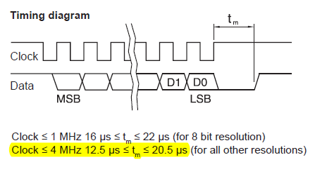
The timing diagram presented in the datasheet is as follows:

Regards.

  • Hello Armin,

    I would suggest you start with one of the SPI examples in C2000ware. Please look in the following folder:

    <c2000ware_install_folder>\driverlib\f2837xd\examples\cpu1\spi

    I would suggest you modify the spi_ex3_external_loopback_fifo_interrupts.c example. Please refer to the device technical reference manual for an explanation of the SPI peripheral. You can always search or post the E2E forum for any questions regarding the operation of the SPI module.

  • Thanks for the reply.

    I have actually read the TRM and have searched the forum but still have some issues in performing SPI.

    For the mentioned application, should I use 3-wire mode? Should I use FIFO mode? Why this encoder does not use chip-select?

    For starting with SPI, I have worked with the ControlSUITE example but I am a little confused. Thanks for your suggestion. I am going to look at the examples of C2000ware.

    Would you please help me with my above-mentioned issues?

    Regards

  • Hi Armin,

    I'm making some assumptions from your timing diagram:

    - Clock generated by master

    - Data generated by master (i.e. one-way communication)

    If this is the case, then you can use SPI in master mode. The 3-wire mode is only used when implementing bidirectional communication on the data line. Based on my assumption above this is not the case, therefore 3-wire mode is not needed. Connect SOMI line and leave MOSI data line unconnected.

    The tm restriction leads me to believe that you need to give some time between data transfers, therefore you will need to control the back-to-back timing of SPI transfers in your code. There is a SPI transfer delay feature which may help & you can read more about in the TRM.

    FIFO mode is optional. The benefit is that it decreases the number of interrupts generated to the CPU. 

    Chip-select doesn't have to be used in SPI master mode if the slave device doesn't need it. Why the encoder doesn't need it, I am not sure. 

    Here is a thread on encoders which may be useful.

    https://e2e.ti.com/support/microcontrollers/c2000/f/171/p/880443/3258315#3258315

  • Thanks for the reply,

    In the TRM, the "Delayed transfer" topic is discussed under the "SPI FIFO Description" topic. So do I have to enable the FIFO mode to generat a delay between the clock cycles and to use the "Delayed transfer" feature? 

    Regards.

  • Armin Miremad said:
    So do I have to enable the FIFO mode to generat a delay between the clock cycles and to use the "Delayed transfer" feature? 

    Yes, that is correct.

  • Thanks again for the reply.

    I am working with the ControlSUITE "spi_loopback" example. As you said, by increasing the value written to SPIFFCT register (TXDLY), the delay is increased. However, there is always a delay between the clock cycle even when I let TXDLY=0. Why this delay exists? Is it always constant?

    Would you please let me know how the example changes "SPISTE" pin logic level? I can't find anything related in the code. 

    Regards.

  • Armin,

    I'm assuming you are looking at this example:

    \controlSUITE\device_support\F2837xD\v210\F2837xD_examples_Cpu1\spi_loopback\cpu01\Example_2837xDSpi_FFDLB.c

    Unless you have modified the flow if the example, you can see that it waits until the transmitted value is received before loading the next value. This likely why you are seeing that gap between clock cycles.

       for(;;)
       {
            //
            // Transmit data
            //
            spi_xmit(sdata);
    
            //
            // Wait until data is received
            //
            while(SpiaRegs.SPIFFRX.bit.RXFFST !=1) { }
    
            //
            // Check against sent data
            //
            rdata = SpiaRegs.SPIRXBUF;
            if(rdata != sdata)
            {
                error();
            }
            sdata++;
       }

    To see the TXDLY at work you have to modify the example code to load more than one value into the FIFO. In other words, make multiple back-to-back calls to spi_xmit(). Note, you will have to update the rest of the code to make sure the CPU reads multiple values from the RX FIFO.

  • Thanks again for the reply,

    Yes, you are right. I'm dealing with your mentioned example.

    - As there is no delay in the coding for sending the data, is it correct to conclude that this delay stands for the data to be transmitted from the SPIDAT to SPIRXBUF after a complete clock cycle? Is this delay always constant?

    - Would you please let me know how the example changes "SPISTE" pin logic level? I can't find anything related in the code. However, I can see that the signal related to this pin changes after a clock cycle.

    regards.

  • Hello,

    Armin Miremad said:
    - As there is no delay in the coding for sending the data, is it correct to conclude that this delay stands for the data to be transmitted from the SPIDAT to SPIRXBUF after a complete clock cycle? Is this delay always constant?

    There is a delay in the code. Roughly it works like this:

    1. CPU loads data into SPITXBUF (call to spi_xmit())

    2. CPU then waits for SPI to finish receiving data (checks RXFFST)

    3. CPU then reads data off SPIRXBUF, checks data, updates counter

    4. Restarts from step 1.

    Step 3 creates a delay between SPI transfers. Try calling spi_xmit() back to back and you'll see two characters transmitted with no delay between them.

    - Would you please let me know how the example changes "SPISTE" pin logic level? I can't find anything related in the code. However, I can see that the signal related to this pin changes after a clock cycle.

    You will need to operate the SPISTE pin in GPIO mode (pinmux configuration). Then you can control the state of the GPIO pin directly from the CPU. You can refer to any of the GPIO examples in ControlSUITE to see how the GPIO is configured and used.

  • Sorry, after re-reading I realized I may have misunderstood your second question. The SPI will automatically control the SPISTE pin. It will drive the SPISTE pin low during a transfer, and drive it high after the transfer is done.

  • Thanks for the reply.

    I got it. So it works automatically and so no need to take care of it during working with SPI.

    Regards.