This thread has been locked.

If you have a related question, please click the "Ask a related question" button in the top right corner. The newly created question will be automatically linked to this question.

TMS320F28388D: ADC pin jump when it sample

Part Number: TMS320F28388D
Other Parts Discussed in Thread: TINA-TI

Hi

I'm testing 28388 ADC with adc_ex5_soc_continuous example.
Circuits based on control card, Using REF5030 for reference.
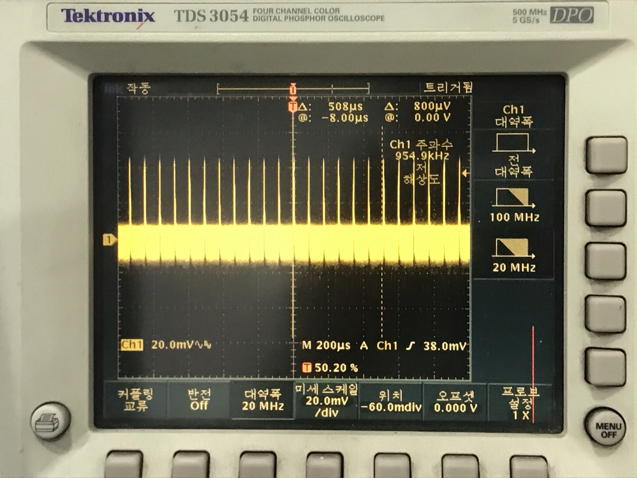
I connected two 1Kohm between ADCINB0 - GND, ADCINB0 - 3.3V to get 1.65V
Here is the sample result, about 20 LSB fluctuation.

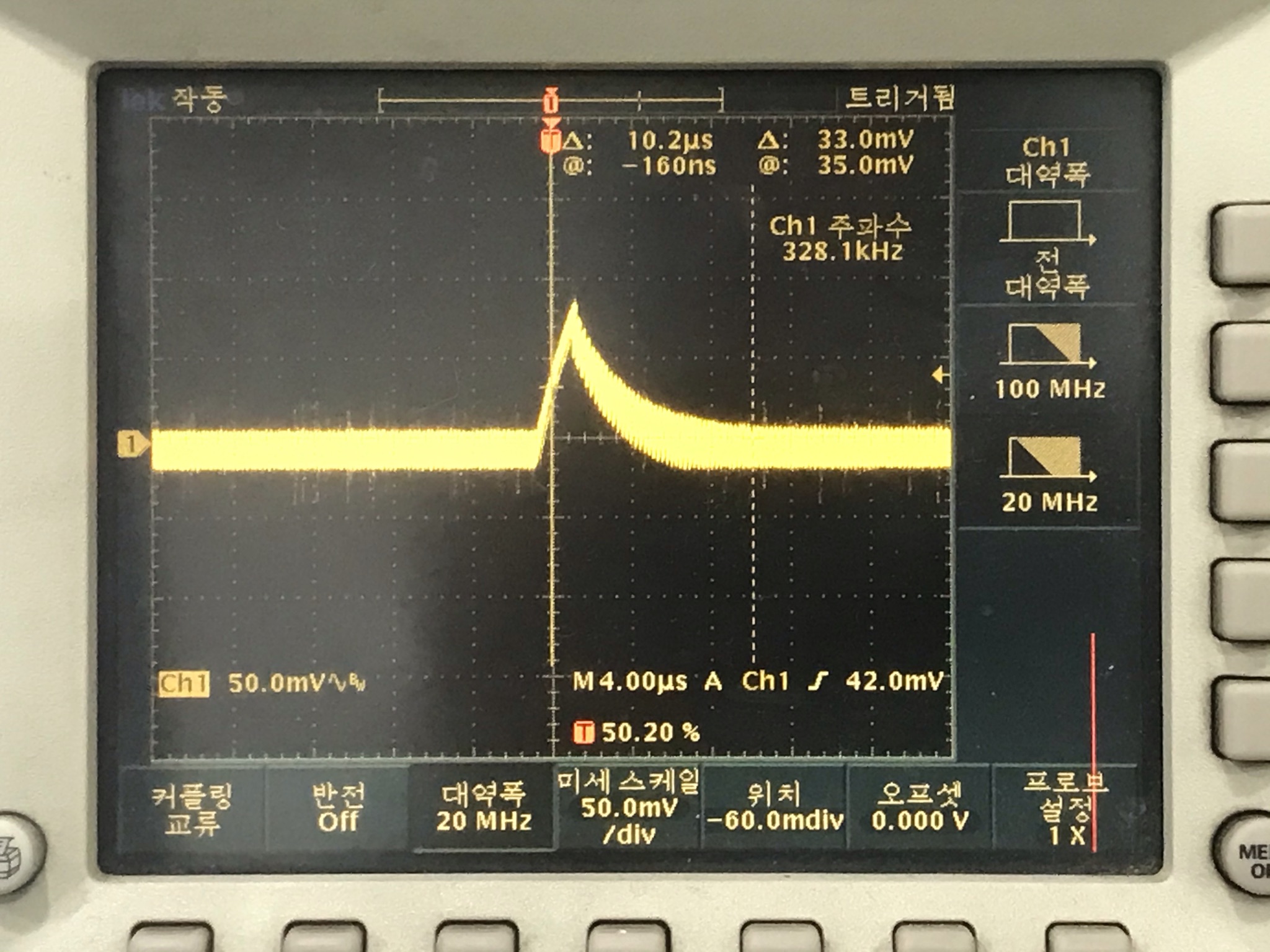
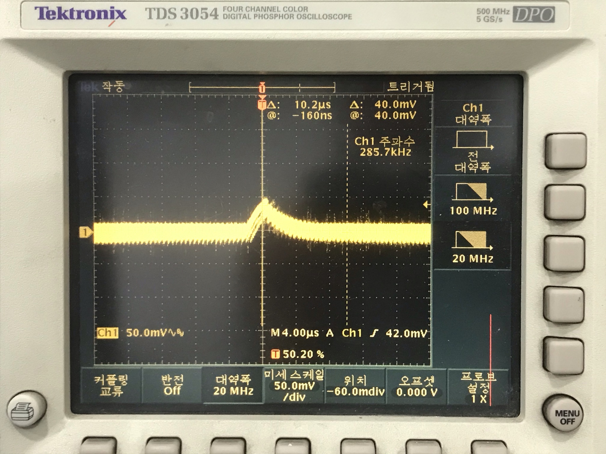
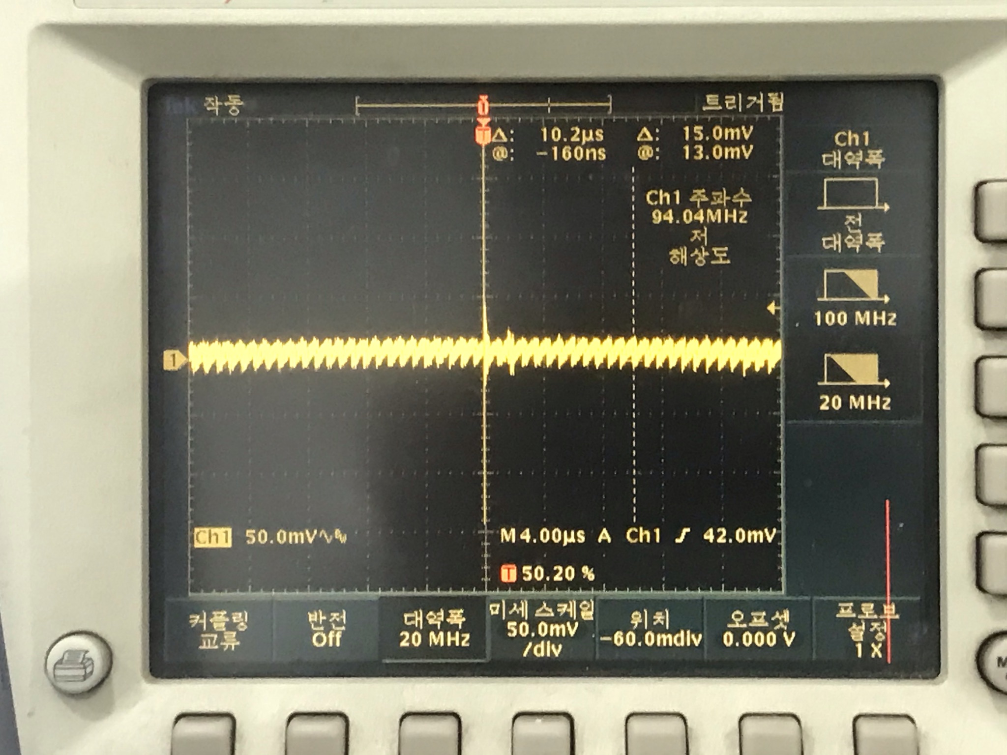
But I wonder why ADCIN PIN jump 50mV on oscilloscope
when it sample. while 3.3VA & ref pin still clean on oscilloscope.

I tried several acqps 8 / 63 / 125. 125 looks good, but only 8 gets less than 9 LSB flux, while the other 20 LSB.

Is it predictable normal phenomenon?

Is there any method that can improve it?

Regards

Kim taeyeong

  • Hi Taeyeong,

    See a description of the ADC sampling process and normal design of ADC driving circuits here:  https://www.ti.com/lit/an/spract6/spract6.pdf.

    The ADC input is a switched capacitor circuit.  When the ADC samples, the first thing that happens is that the internal S+H capacitor equalizes with any external capacitor on the ADC pin.  In your case, I think the only capacitance on the pin is the parasitic capacitance of the PCB and the capacitance of your scope probe, so the equalization creates a relatively large glitch. You should see a lower glitch if you add some capacitance on the pin.  A good starting point may be 200-300pF.  

    As far as the 20LSBs of noise in the sampled results, consider

    • The 3.3V rail isn't a particularly clean voltage source
    • Your effective source impedance is 1kohms || 1kohms = 500 ohms.  You'll likely need a very long S+H window duration (set by acqps field of SOC configuration register).  See the "choosing an acquisition window duration" section of the TRM for a quick estimate of the required duration or the app. note linked above for how to simulate using TINA-TI to determine the required duration. 
    • Adding additional capacitance to the pin may help reduce the noise by adding some low-pass filtering.  However, increasing this will also result in slower settling, so you may also need to increase ACQPS / settling time (see previous point about how to determine the settling time). 
    • Attaching the scope probe to the channel while sampling is a potential path for noise to couple in.  You may want to try to sampling without the scope probe connected and determine if this reduces the noise
    • It isn't clear if you are using wires + through hole resistors to create your circuit, or if this is fabricated on a PCB.  If using wires and discrete components to create a prototype, try to keep the wire lengths as short as possible to reduce paths for noise to couple in.

  • I added some decoupling to 3.3VA & adjust acqps to 12,

    And I got +-1~2LSB of noise on 12bit mode.

    But I still wonder why I need the first 20 sample till stabilize?

    Is it predictable with adc_ex5_soc_continuous ?

  • Hi Kim,

    I think if you use the equations in the "choosing an acquisition window duration" section of the TRM () you'll get a longer S+H window requirement than 5ns*(12 + 1 )SYSCLKs = 65ns.  In fact, 65ns doesn't even meet the minimum value for the device (75ns), which would only be applicable in case of a very low impedance and high bandwidth driver.  You can also use the simulation methods in the linked app. note to determine the required S+H time.

    As for the stabilization over multiple cycles, see the section "Charge Sharing Example" in section 4.1 in the app. note that was originally linked.  You should be able to build and simulate your circuit using the methods in the app. note to determine the expected behavior.