This thread has been locked.

If you have a related question, please click the "Ask a related question" button in the top right corner. The newly created question will be automatically linked to this question.

LAUNCHXL-F28379D: External Power Supply and debug via USB with "adc_ex1_soc_software" example

Part Number: LAUNCHXL-F28379D

Hi,

i tried to supply the board with an external voltage generator. But the adc values are not as expected.

First i tried the "adc_ex1_soc_software" example for testing with power supply from USB (no external source). I connected the generators ground to the ground above Pin 23. The signal of the generator to PIN 30. I watched the adcAResult0 in CCS with the "Graph" tool while i used a sinusoidal function (1Vpp with 500mV offset -> 0V to 1V ).

It works - see picture 1. (I'm just wondering that the voltage seen by the controller is below zero - with an osziloskop it is exactly 0 to 1 V..maybe someone can help me with that too?) 
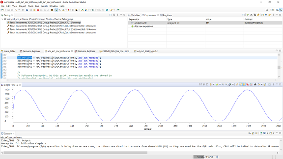

Now i disconnected JP1, JP2 and JP3 (JP6 is disconnected too). I used the pins from JP1 and JP2 to give the board a voltage supply of approximately of 3.3V (2.95 to 3.35).. LEDs are on - everything seems to be okay. Same example without problems while debugging.

I used again the adcAResult0 (Pin 30) to watch the ADCs input and it switches just between zero and max (4095). -> See picture 2.
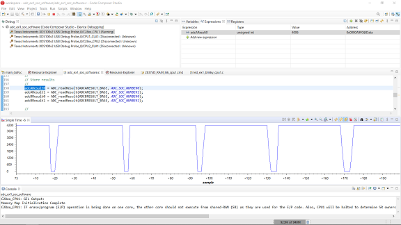
I tried some other things like a voltage divider between the ground and 3.3V of the supply and measuring the divided voltage - the result is the same. I can only measure the maximum value of 4095 or zero.

Where is my fallacy? Can someone help me?

Thanks a lot.

Benjamin

  • Benjamin Hoepfner said:
    It works - see picture 1. (I'm just wondering that the voltage seen by the controller is below zero - with an osziloskop it is exactly 0 to 1 V..maybe someone can help me with that too?) 

    Did you observe the signal on scope while the example was running?  There might be some unexpected influence while the running system.

    It would also be a good idea to confirm the input and conversion levels using a DC signal first.  You can also probe the VREFHI signals to inspect the full-scale voltage provided to the ADC for better context.

    Benjamin Hoepfner said:
    I used the pins from JP1 and JP2 to give the board a voltage supply of approximately of 3.3V (2.95 to 3.35)

    Are you supplying 5V to the board as well?  Some components on the board use the 5V supply.  You can see the User Guide for external supply configurations and schematics.

  • Hi,

    many thanks for your fast response.

    > Did you observe the signal on scope while the example was running?  There might be some unexpected influence while the running system. -> OK

    Yes, you are right - there is an influence if i observe the signal while running the example. But thats not the main aspect of my problem.  I examind my setup a little bit and i recognized, that the output impedance of my signal generator is 50Ohms. I think, that the impedance of the adc input is much higher (no matching) and thats one reason, why i measure not the expected signal with my adc.

    By using an "old & heavy" analog DC source i can measure the voltage that i expect. Thanks for that hint! The question i'm asking myself with that knowledge is - how can i make sure that a i measure the right value in a motor control for example..

    > Are you supplying 5V to the board as well?  Some components on the board use the 5V supply.  You can see the User Guide for external supply configurations and schematics. -> OK

    That was a really good indication, I read the instructions, but not in enough detail. I forgot to short pin JP6 - it's important for the 5V supply on the board as you assumed. Now I can measure in an acceptable manner with an external power supply of 3.3V.

    Summerized for others with that problem:

    - Open the jumpers on JP1, JP2, JP3

    - Supply the board side on JP1 and JP2 with an external signal of 3,3V or higher (not too high..)

    - Short the jumper JP6 for on board 5V power supply

    - Connect via USB and have fun

    >You can also probe the VREFHI signals to inspect the full-scale voltage provided to the ADC for better context.

    Yes i thats what i would like to do - can you explain how to probe the VREFHI voltage? I thought, that VREFHI is the same voltage that i can measure on Pin 1 - the 3.3V Pin. I can measure a voltage of 3.232V via USB supply (measured with a fluke multimeter). Thats seems a little bit arbitrary ? Is that the value of VREFHI ?

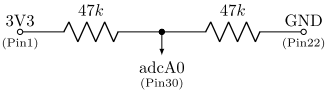
    In a little experimental setup i used the 3.3V Pin (1) through a voltage divider (two same resistors in a row) to a ground Pin (22). With the adcA0 i measured the divided voltage. I ecpected a value of 4095/2 but the result is much less than this.

    Is there anyone who can help me with this last problem?

    Thanks a lot.

    Benjamin

  • Benjamin Hoepfner said:
    can you explain how to probe the VREFHI voltage?

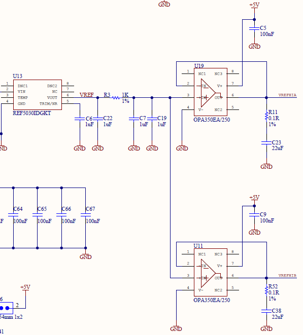
    You can see the schematic for potential components and points to probe.  R3, R11, and R52 would be good candidates:

    Benjamin Hoepfner said:
    I thought, that VREFHI is the same voltage that i can measure on Pin 1 - the 3.3V Pin. I can measure a voltage of 3.232V via USB supply (measured with a fluke multimeter). Thats seems a little bit arbitrary ? Is that the value of VREFHI ?

    No, you can see in the schematic that VREFHI is independently generated using a high-precision REF5x device and buffered using op-amps.

    You can find information about how VREFHI contributes to expected ADC conversions in the TRM.

    Benjamin Hoepfner said:
    In a little experimental setup i used the 3.3V Pin (1) through a voltage divider (two same resistors in a row) to a ground Pin (22).

    Voltage dividers can contribute errors to conversions if not handled correctly.  You can see the "Choosing an Acquisition Window Duration" section in the TRM or this appnote for guidance.

  • Many thanks,

    that helped a lot!