This thread has been locked.

If you have a related question, please click the "Ask a related question" button in the top right corner. The newly created question will be automatically linked to this question.

TMS320F28377D: ePWM generation using CLB Tool

Part Number: TMS320F28377D
Other Parts Discussed in Thread: C2000WARE, CONTROLSUITE

Hi,

I am trying the CLB tool for the first time to generate a customised ePWM signal using already produced two other ePWM signals; PWM1 and PWM2.

The third signal which I want to produce (PWM3) should be based on the below logic:

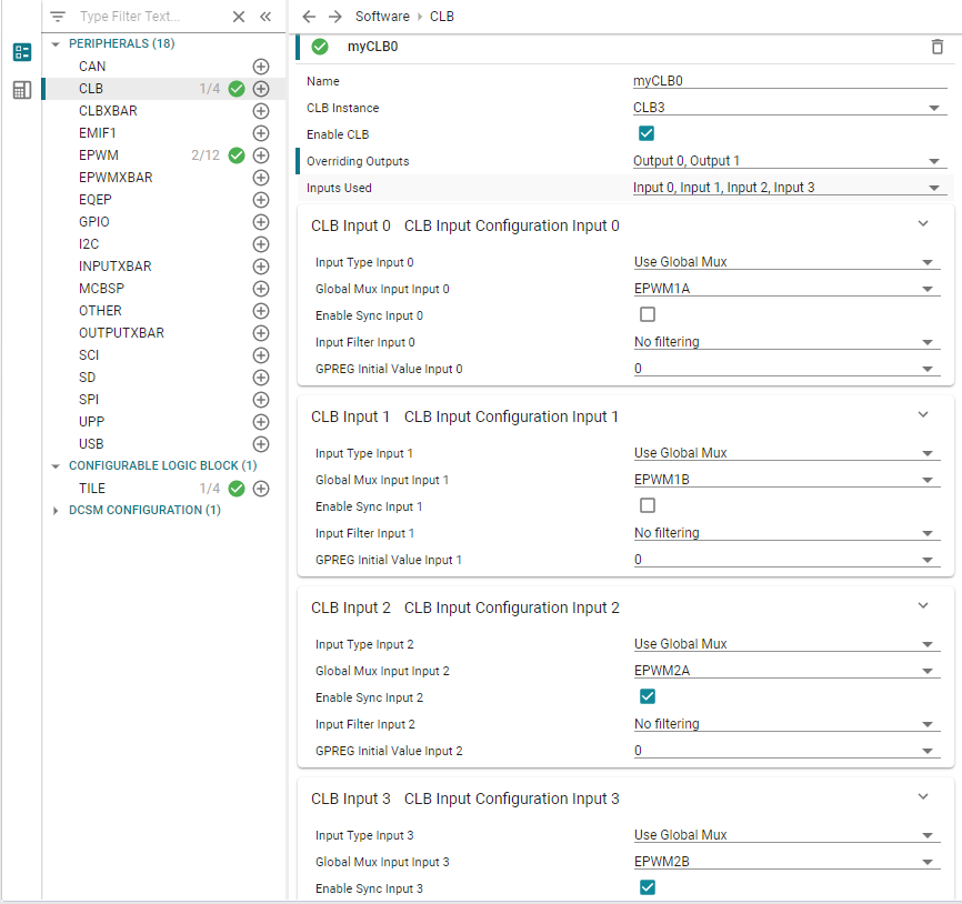
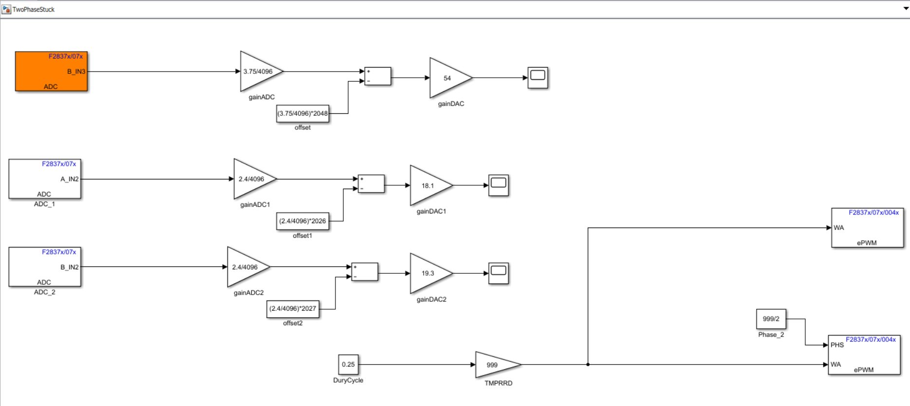
(PWM3A= PWM1A XOR PWM2A ), and (PWM3B =PWM1A  NXOR PWM2A )

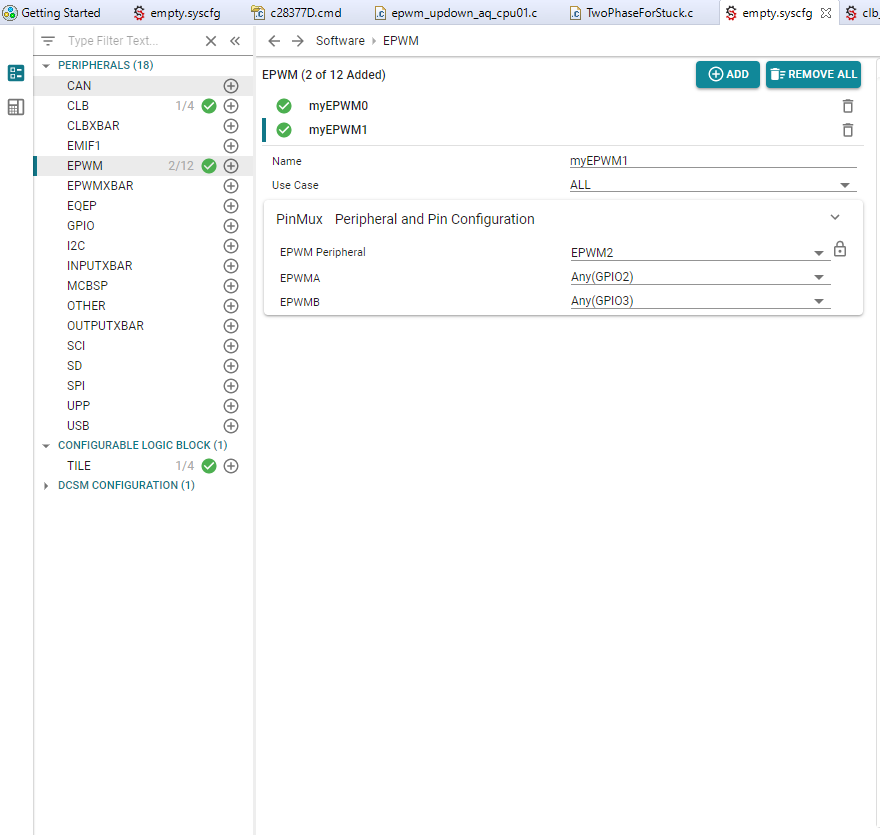
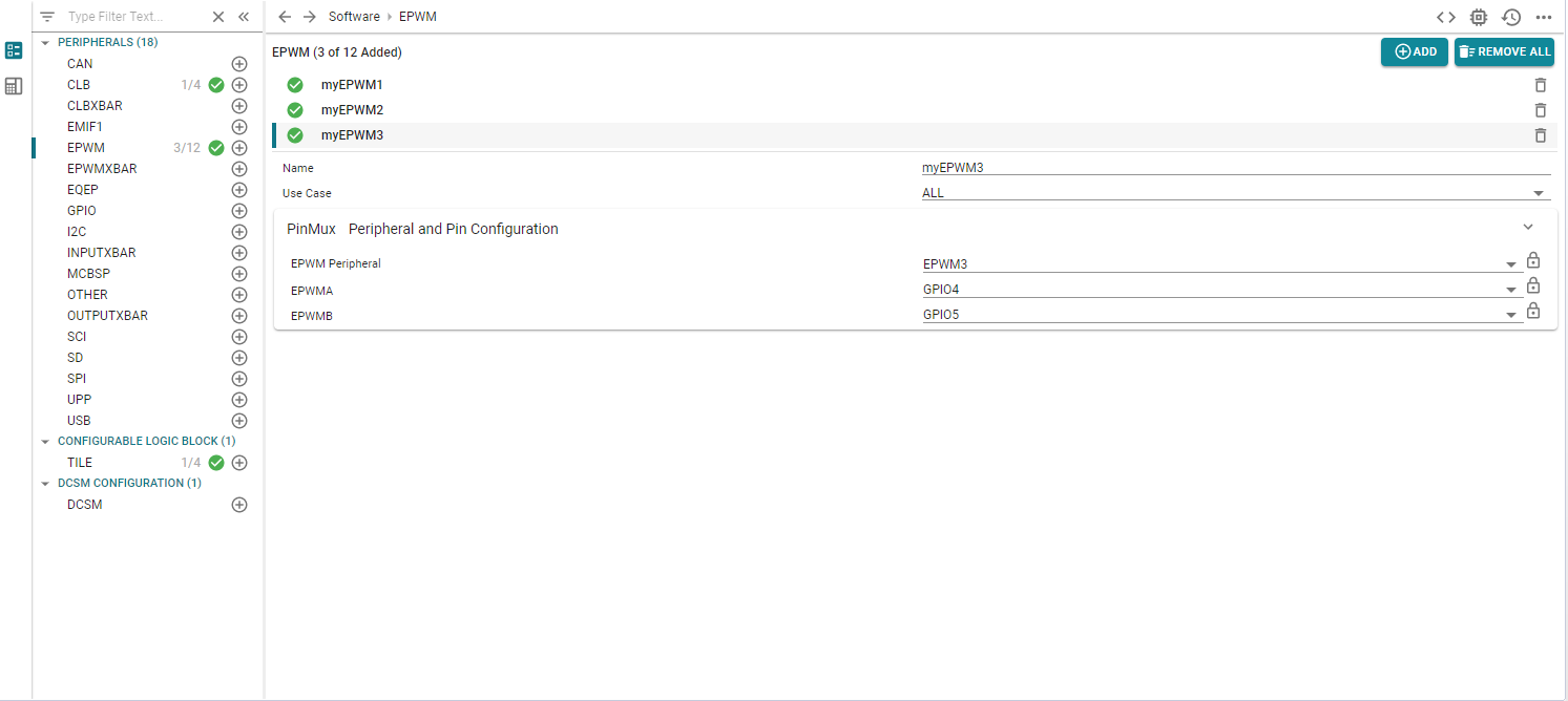
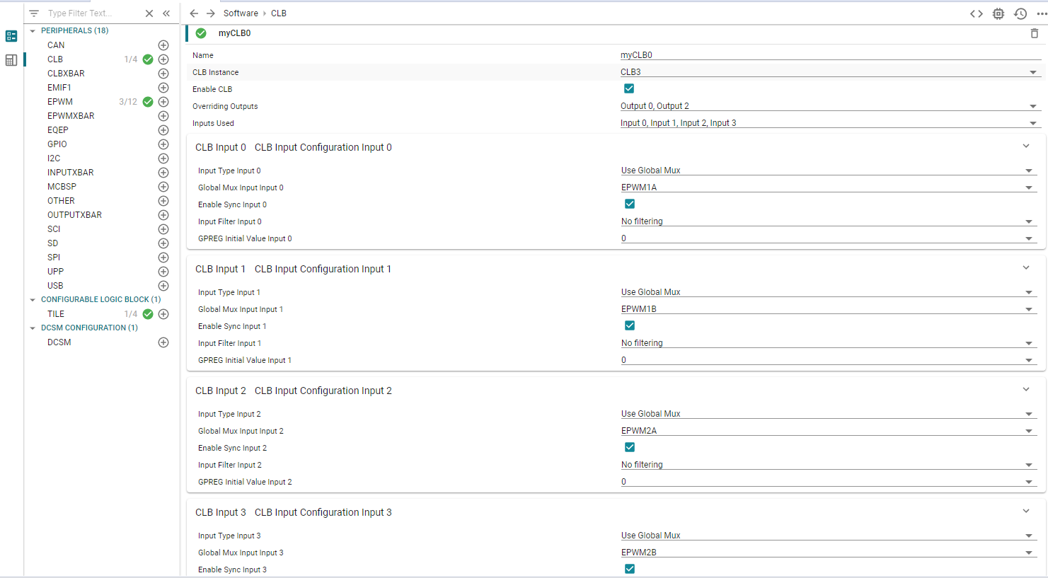
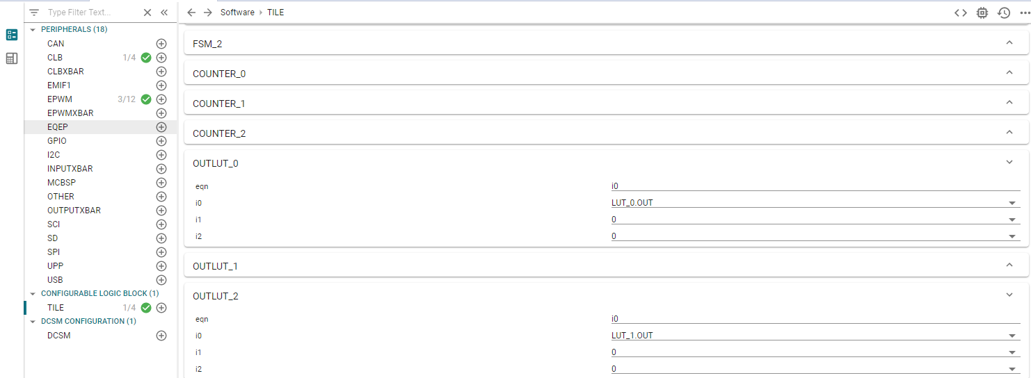
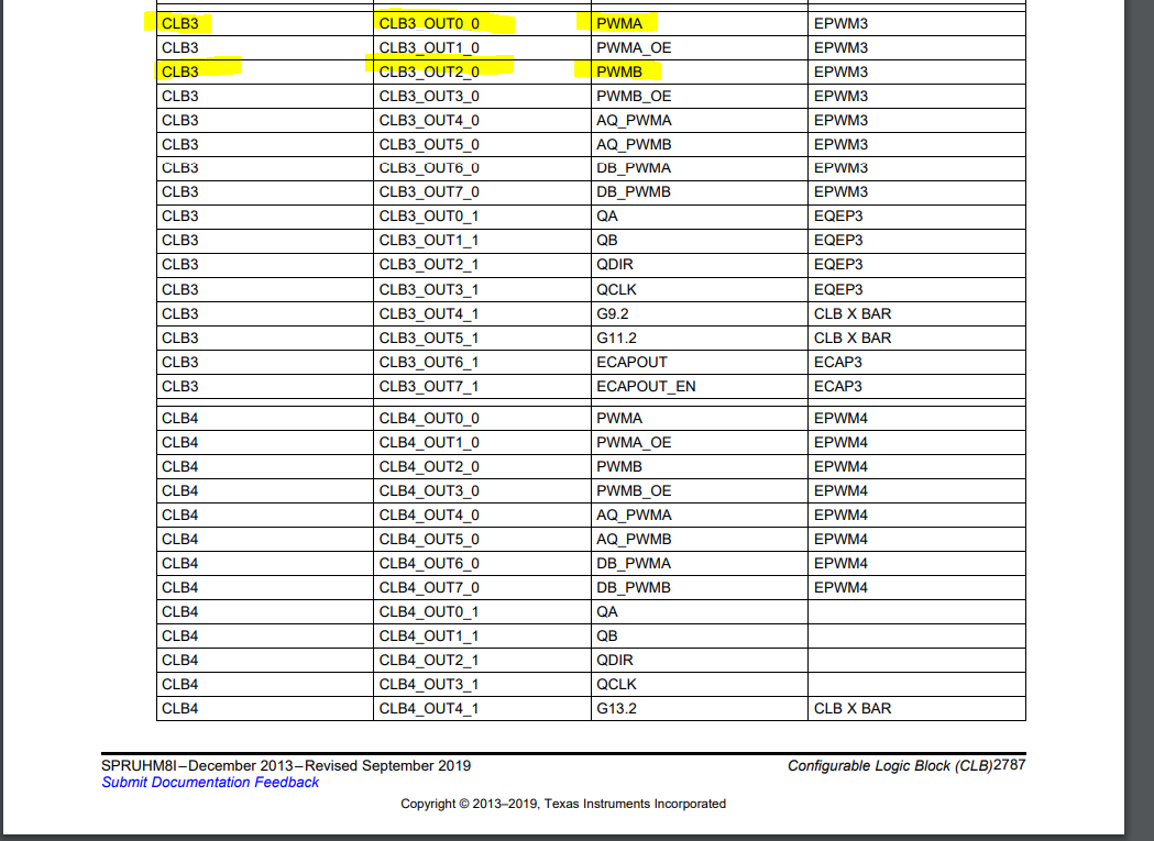
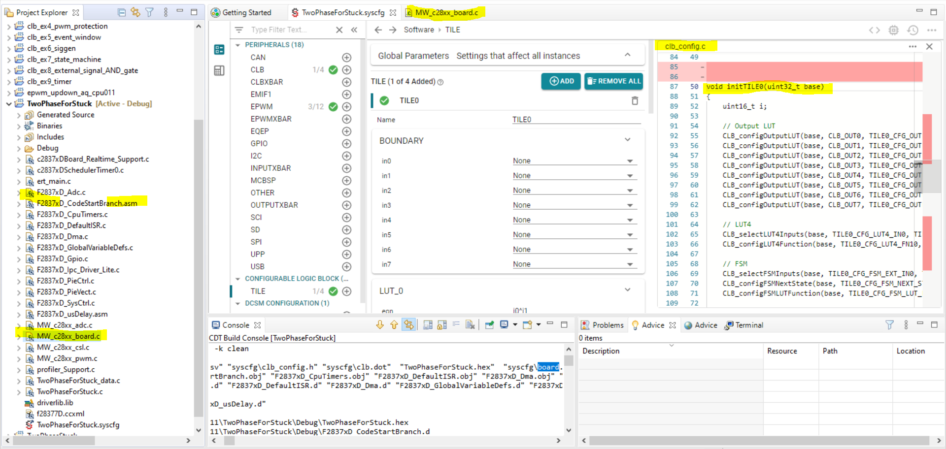
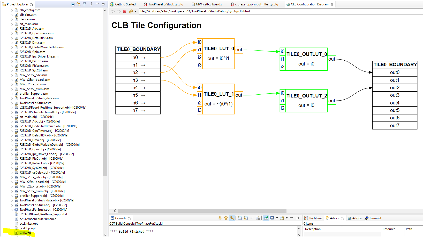
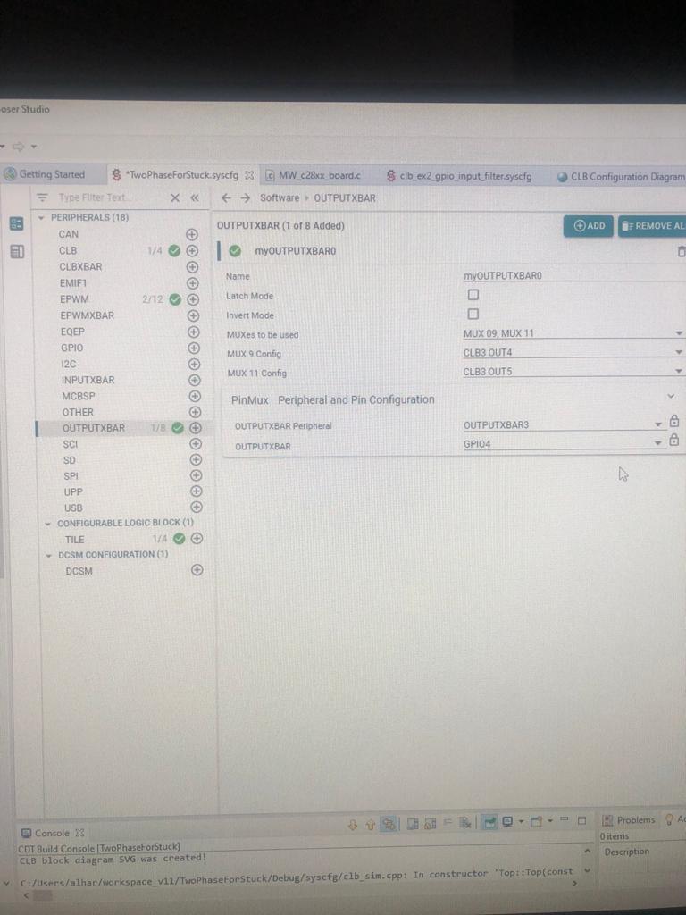
I made an attempt to access EPWM1,2,3 through the CLB, and I use the (EPWM1A, EPWM2A, EPWM1B, EPWM2B) as inputs to a CLB TILE (Use CLB3), then I implemented the logic inside a LUT of the CLB module, then output the signal onto EPWM3A & EPWM3B through the CLB OUTPUT INTERSECT (override).

So please let me know if my below steps are correct?

Regards,

Mohammed 


  • You don't have EPWM3 in the EPWM module. You need to add that and make sure to pick the GPIOs for EPWM3. The CLB will show up on those pins/GPIOs after output intersect.

    Also enable SYNCHRONIZER on all CLB inputs.

    Otherwise great job and keep up the good work!

    Nima

  • Thanks Nima for your unlimited help, can't thank you enough!

    I followed your steps but still couldn't get any signal coming out from GPIO4(ePWM3A) and GPIO(ePWM3B). I am a bit not sure of how to select the proper inputs for the LUT blocks in such a way that the Global Mux Inputs assigned in the CLB are selected as inputs for the LUT blocks? Do I have to include them first in the boundary block?

    Also, I have made some search and found out how to determine which specific CLB Output Signal I should select to trigger PWM3A and PWM3B. using the Technical Reference Manual I selected output 0 and output 2 as attached in the pictures.

    So please let me know if I missing anything?

    Regards, 

  • Everything I see now looks correct. 

    For your CLB TILE BOUNDARY0 = CLB INPUT0 and so on. You have that correctly. You also have the correct CLB TILE OUTs being used. CLB3 OUT0 will override EPWM3A and OUT2 will override EPWM3B.

    In your C code in main, which should be very short, what are the functions you are calling?

    Nima

  • Hi Nima,

    The C code is generated using MATLAB Simulink as I told you earlier. I could see the signals ePWM1 and ePWM2 and have no issue with that.

    Here is my main C cdoe:

    #include "TwoPhaseForStuck.h"
    #include "rtwtypes.h"
    
    volatile int IsrOverrun = 0;
    static boolean_T OverrunFlag = 0;
    void rt_OneStep(void)
    {
      /* Check for overrun. Protect OverrunFlag against preemption */
      if (OverrunFlag++) {
        IsrOverrun = 1;
        OverrunFlag--;
        return;
      }
    
      enableTimer0Interrupt();
      TwoPhaseForStuck_step();
    
      /* Get model outputs here */
      disableTimer0Interrupt();
      OverrunFlag--;
    }
    
    volatile boolean_T stopRequested = false;
    int main(void)
    {
      volatile boolean_T runModel = true;
      float modelBaseRate = 1.25E-6;
      float systemClock = 200;
      c2000_flash_init();
      init_board();
    
    #ifdef MW_EXEC_PROFILER_ON
    
      config_profilerTimer();
    
    #endif
    
      ;
      rtmSetErrorStatus(TwoPhaseForStuck_M, 0);
      TwoPhaseForStuck_initialize();
      configureTimer0(modelBaseRate, systemClock);
      runModel =
        rtmGetErrorStatus(TwoPhaseForStuck_M) == (NULL);
      enableTimer0Interrupt();
      globalInterruptEnable();
      while (runModel) {
        stopRequested = !(
                          rtmGetErrorStatus(TwoPhaseForStuck_M) == (NULL));
        runModel = !(stopRequested);
      }
    
      /* Disable rt_OneStep() here */
    
      /* Terminate model */
      TwoPhaseForStuck_terminate();
      globalInterruptDisable();
      return 0;
    }
    
    /*
     * File trailer for generated code.
     *
     * [EOF]
     */
    

    The other c-fil is as follows:

    #include "TwoPhaseForStuck.h"
    #include "TwoPhaseForStuck_private.h"
    
    /* Block signals (default storage) */
    B_TwoPhaseForStuck_T TwoPhaseForStuck_B;
    
    /* Real-time model */
    RT_MODEL_TwoPhaseForStuck_T TwoPhaseForStuck_M_;
    RT_MODEL_TwoPhaseForStuck_T *const TwoPhaseForStuck_M = &TwoPhaseForStuck_M_;
    static uint16_T adcBInitFlag = 0;
    static uint16_T adcAInitFlag = 0;
    
    /* Model step function */
    void TwoPhaseForStuck_step(void)
    {
      /* local block i/o variables */
      real_T rtb_TMPRRD;
    
      /* S-Function (c2802xadc): '<Root>/ADC' */
      {
        /*  Internal Reference Voltage : Fixed scale 0 to 3.3 V range.  */
        /*  External Reference Voltage : Allowable ranges of VREFHI(ADCINA0) = 3.3 and VREFLO(tied to ground) = 0  */
        TwoPhaseForStuck_B.ADC = (AdcbResultRegs.ADCRESULT1);
      }
    
      /* S-Function (c2802xadc): '<Root>/ADC_1' */
      {
        /*  Internal Reference Voltage : Fixed scale 0 to 3.3 V range.  */
        /*  External Reference Voltage : Allowable ranges of VREFHI(ADCINA0) = 3.3 and VREFLO(tied to ground) = 0  */
        TwoPhaseForStuck_B.ADC_1 = (AdcaResultRegs.ADCRESULT0);
      }
    
      /* S-Function (c2802xadc): '<Root>/ADC_2' */
      {
        /*  Internal Reference Voltage : Fixed scale 0 to 3.3 V range.  */
        /*  External Reference Voltage : Allowable ranges of VREFHI(ADCINA0) = 3.3 and VREFLO(tied to ground) = 0  */
        TwoPhaseForStuck_B.ADC_2 = (AdcbResultRegs.ADCRESULT0);
      }
    
      /* Gain: '<Root>/TMPRRD' incorporates:
       *  Constant: '<Root>/DuryCycle'
       */
      rtb_TMPRRD = TwoPhaseForStuck_P.TMPRRD_Gain *
        TwoPhaseForStuck_P.DuryCycle_Value;
    
      /* S-Function (c2802xpwm): '<Root>/ePWM4' */
    
      /*-- Update CMPA value for ePWM1 --*/
      {
        EPwm1Regs.CMPA.bit.CMPA = (uint16_T)(rtb_TMPRRD);
      }
    
      /* S-Function (c2802xpwm): '<Root>/ePWM5' incorporates:
       *  Constant: '<Root>/Phase_2'
       */
      EPwm2Regs.TBPHS.bit.TBPHS = TwoPhaseForStuck_P.Phase_2_Value;
    
      /*-- Update CMPA value for ePWM2 --*/
      {
        EPwm2Regs.CMPA.bit.CMPA = (uint16_T)(rtb_TMPRRD);
      }
    }
    
    /* Model initialize function */
    void TwoPhaseForStuck_initialize(void)
    {
      /* Registration code */
    
      /* initialize error status */
      rtmSetErrorStatus(TwoPhaseForStuck_M, (NULL));
    
      /* block I/O */
      (void) memset(((void *) &TwoPhaseForStuck_B), 0,
                    sizeof(B_TwoPhaseForStuck_T));
    
      /* Start for S-Function (c2802xadc): '<Root>/ADC' */
      if (adcBInitFlag == 0) {
        InitAdcB();
        adcBInitFlag = 1;
      }
    
      config_ADCB_SOC1 ();
    
      /* Start for S-Function (c2802xadc): '<Root>/ADC_1' */
      if (adcAInitFlag == 0) {
        InitAdcA();
        adcAInitFlag = 1;
      }
    
      config_ADCA_SOC0 ();
    
      /* Start for S-Function (c2802xadc): '<Root>/ADC_2' */
      if (adcBInitFlag == 0) {
        InitAdcB();
        adcBInitFlag = 1;
      }
    
      config_ADCB_SOC0 ();
    
      /* Start for S-Function (c2802xpwm): '<Root>/ePWM4' */
      EALLOW;
      CpuSysRegs.PCLKCR2.bit.EPWM1 = 1;
      CpuSysRegs.PCLKCR0.bit.TBCLKSYNC = 0;
      EDIS;
    
      /*** Initialize ePWM1 modules ***/
      {
        /*  // Time Base Control Register
           EPwm1Regs.TBCTL.bit.CTRMODE              = 0;          // Counter Mode
           EPwm1Regs.TBCTL.bit.SYNCOSEL             = 1;          // Sync Output Select
           EPwm1Regs.TBCTL.bit.PRDLD                = 0;          // Shadow select
           EPwm1Regs.TBCTL.bit.PHSEN                = 0;          // Phase Load Enable
           EPwm1Regs.TBCTL.bit.PHSDIR               = 0;          // Phase Direction Bit
           EPwm1Regs.TBCTL.bit.HSPCLKDIV            = 0;          // High Speed TBCLK Pre-scaler
           EPwm1Regs.TBCTL.bit.CLKDIV               = 0;          // Time Base Clock Pre-scaler
           EPwm1Regs.TBCTL.bit.SWFSYNC              = 0;          // Software Force Sync Pulse
         */
        EPwm1Regs.TBCTL.all = (EPwm1Regs.TBCTL.all & ~0x3FFF) | 0x10;
    
        /*-- Setup Time-Base (TB) Submodule --*/
        EPwm1Regs.TBPRD = 999;             // Time Base Period Register
    
        /* // Time-Base Phase Register
           EPwm1Regs.TBPHS.bit.TBPHS               = 0;          // Phase offset register
         */
        EPwm1Regs.TBPHS.all = (EPwm1Regs.TBPHS.all & ~0xFFFF0000) | 0x0;
    
        // Time Base Counter Register
        EPwm1Regs.TBCTR = 0x0000;          /* Clear counter*/
    
        /*-- Setup Counter_Compare (CC) Submodule --*/
        /*	// Counter Compare Control Register
           EPwm1Regs.CMPCTL.bit.SHDWAMODE           = 0;  // Compare A Register Block Operating Mode
           EPwm1Regs.CMPCTL.bit.SHDWBMODE           = 0;  // Compare B Register Block Operating Mode
           EPwm1Regs.CMPCTL.bit.LOADAMODE           = 0;          // Active Compare A Load
           EPwm1Regs.CMPCTL.bit.LOADBMODE           = 0;          // Active Compare B Load
         */
        EPwm1Regs.CMPCTL.all = (EPwm1Regs.CMPCTL.all & ~0x5F) | 0x0;
    
        /* EPwm1Regs.CMPCTL2.bit.SHDWCMODE           = 0;  // Compare C Register Block Operating Mode
    
           EPwm1Regs.CMPCTL2.bit.SHDWDMODE           = 0;  // Compare D Register Block Operating Mode
         */
        EPwm1Regs.CMPCTL2.all = (EPwm1Regs.CMPCTL2.all & ~0x50) | 0x0;
        EPwm1Regs.CMPA.bit.CMPA = 0;       // Counter Compare A Register
        EPwm1Regs.CMPB.bit.CMPB = 0;       // Counter Compare B Register
        EPwm1Regs.CMPC = 0;                // Counter Compare C Register
        EPwm1Regs.CMPD = 0;                // Counter Compare D Register
    
        /*-- Setup Action-Qualifier (AQ) Submodule --*/
        EPwm1Regs.AQCTLA.all = 33;         // Action Qualifier Control Register For Output A
        EPwm1Regs.AQCTLB.all = 96;         // Action Qualifier Control Register For Output B
    
        /*	// Action Qualifier Software Force Register
           EPwm1Regs.AQSFRC.bit.RLDCSF              = 0;          // Reload from Shadow Options
         */
        EPwm1Regs.AQSFRC.all = (EPwm1Regs.AQSFRC.all & ~0xC0) | 0x0;
    
        /*	// Action Qualifier Continuous S/W Force Register
           EPwm1Regs.AQCSFRC.bit.CSFA               = 0;          // Continuous Software Force on output A
           EPwm1Regs.AQCSFRC.bit.CSFB               = 0;          // Continuous Software Force on output B
         */
        EPwm1Regs.AQCSFRC.all = (EPwm1Regs.AQCSFRC.all & ~0xF) | 0x0;
    
        /*-- Setup Dead-Band Generator (DB) Submodule --*/
        /*	// Dead-Band Generator Control Register
           EPwm1Regs.DBCTL.bit.OUT_MODE             = 3;          // Dead Band Output Mode Control
           EPwm1Regs.DBCTL.bit.IN_MODE              = 0;          // Dead Band Input Select Mode Control
           EPwm1Regs.DBCTL.bit.POLSEL               = 2;          // Polarity Select Control
           EPwm1Regs.DBCTL.bit.HALFCYCLE            = 0;          // Half Cycle Clocking Enable
         */
        EPwm1Regs.DBCTL.all = (EPwm1Regs.DBCTL.all & ~0x803F) | 0xB;
        EPwm1Regs.DBRED.bit.DBRED = 20;    // Dead-Band Generator Rising Edge Delay Count Register
        EPwm1Regs.DBFED.bit.DBFED = 20;    // Dead-Band Generator Falling Edge Delay Count Register
    
        /*-- Setup Event-Trigger (ET) Submodule --*/
        /*	// Event Trigger Selection and Pre-Scale Register
           EPwm1Regs.ETSEL.bit.SOCAEN               = 1;          // Start of Conversion A Enable
           EPwm1Regs.ETSEL.bit.SOCASELCMP = 0;
           EPwm1Regs.ETSEL.bit.SOCASEL              = 4 ;          // Start of Conversion A Select
           EPwm1Regs.ETPS.bit.SOCAPRD               = 1;          // EPWM1SOCA Period Select
    
           EPwm1Regs.ETSEL.bit.SOCBEN               = 0;          // Start of Conversion B Enable
    
           EPwm1Regs.ETSEL.bit.SOCBSELCMP = 0;
           EPwm1Regs.ETSEL.bit.SOCBSEL              = 1;          // Start of Conversion A Select
           EPwm1Regs.ETPS.bit.SOCBPRD               = 1;          // EPWM1SOCB Period Select
           EPwm1Regs.ETSEL.bit.INTEN                = 0;          // EPWM1INTn Enable
           EPwm1Regs.ETSEL.bit.INTSELCMP = 0;
           EPwm1Regs.ETSEL.bit.INTSEL              = 4;          // Start of Conversion A Select
    
           EPwm1Regs.ETPS.bit.INTPRD                = 1;          // EPWM1INTn Period Select
         */
        EPwm1Regs.ETSEL.all = (EPwm1Regs.ETSEL.all & ~0xFF7F) | 0x1C04;
        EPwm1Regs.ETPS.all = (EPwm1Regs.ETPS.all & ~0x3303) | 0x1101;
    
        /*-- Setup PWM-Chopper (PC) Submodule --*/
        /*	// PWM Chopper Control Register
           EPwm1Regs.PCCTL.bit.CHPEN                = 0;          // PWM chopping enable
           EPwm1Regs.PCCTL.bit.CHPFREQ              = 0;          // Chopping clock frequency
           EPwm1Regs.PCCTL.bit.OSHTWTH              = 0;          // One-shot pulse width
           EPwm1Regs.PCCTL.bit.CHPDUTY              = 0;          // Chopping clock Duty cycle
         */
        EPwm1Regs.PCCTL.all = (EPwm1Regs.PCCTL.all & ~0x7FF) | 0x0;
    
        /*-- Set up Trip-Zone (TZ) Submodule --*/
        EALLOW;
        EPwm1Regs.TZSEL.all = 0;           // Trip Zone Select Register
    
        /*	// Trip Zone Control Register
           EPwm1Regs.TZCTL.bit.TZA                  = 3;          // TZ1 to TZ6 Trip Action On EPWM1A
           EPwm1Regs.TZCTL.bit.TZB                  = 3;          // TZ1 to TZ6 Trip Action On EPWM1B
           EPwm1Regs.TZCTL.bit.DCAEVT1              = 3;          // EPWM1A action on DCAEVT1
           EPwm1Regs.TZCTL.bit.DCAEVT2              = 3;          // EPWM1A action on DCAEVT2
           EPwm1Regs.TZCTL.bit.DCBEVT1              = 3;          // EPWM1B action on DCBEVT1
           EPwm1Regs.TZCTL.bit.DCBEVT2              = 3;          // EPWM1B action on DCBEVT2
         */
        EPwm1Regs.TZCTL.all = (EPwm1Regs.TZCTL.all & ~0xFFF) | 0xFFF;
    
        /*	// Trip Zone Enable Interrupt Register
           EPwm1Regs.TZEINT.bit.OST                 = 0;          // Trip Zones One Shot Int Enable
           EPwm1Regs.TZEINT.bit.CBC                 = 0;          // Trip Zones Cycle By Cycle Int Enable
           EPwm1Regs.TZEINT.bit.DCAEVT1             = 0;          // Digital Compare A Event 1 Int Enable
           EPwm1Regs.TZEINT.bit.DCAEVT2             = 0;          // Digital Compare A Event 2 Int Enable
           EPwm1Regs.TZEINT.bit.DCBEVT1             = 0;          // Digital Compare B Event 1 Int Enable
           EPwm1Regs.TZEINT.bit.DCBEVT2             = 0;          // Digital Compare B Event 2 Int Enable
         */
        EPwm1Regs.TZEINT.all = (EPwm1Regs.TZEINT.all & ~0x7E) | 0x0;
    
        /*	// Digital Compare A Control Register
           EPwm1Regs.DCACTL.bit.EVT1SYNCE           = 0;          // DCAEVT1 SYNC Enable
           EPwm1Regs.DCACTL.bit.EVT1SOCE            = 1;          // DCAEVT1 SOC Enable
           EPwm1Regs.DCACTL.bit.EVT1FRCSYNCSEL      = 0;          // DCAEVT1 Force Sync Signal
           EPwm1Regs.DCACTL.bit.EVT1SRCSEL          = 0;          // DCAEVT1 Source Signal
           EPwm1Regs.DCACTL.bit.EVT2FRCSYNCSEL      = 0;          // DCAEVT2 Force Sync Signal
           EPwm1Regs.DCACTL.bit.EVT2SRCSEL          = 0;          // DCAEVT2 Source Signal
         */
        EPwm1Regs.DCACTL.all = (EPwm1Regs.DCACTL.all & ~0x30F) | 0x4;
    
        /*	// Digital Compare B Control Register
           EPwm1Regs.DCBCTL.bit.EVT1SYNCE           = 0;          // DCBEVT1 SYNC Enable
           EPwm1Regs.DCBCTL.bit.EVT1SOCE            = 0;          // DCBEVT1 SOC Enable
           EPwm1Regs.DCBCTL.bit.EVT1FRCSYNCSEL      = 0;          // DCBEVT1 Force Sync Signal
           EPwm1Regs.DCBCTL.bit.EVT1SRCSEL          = 0;          // DCBEVT1 Source Signal
           EPwm1Regs.DCBCTL.bit.EVT2FRCSYNCSEL      = 0;          // DCBEVT2 Force Sync Signal
           EPwm1Regs.DCBCTL.bit.EVT2SRCSEL          = 0;          // DCBEVT2 Source Signal
         */
        EPwm1Regs.DCBCTL.all = (EPwm1Regs.DCBCTL.all & ~0x30F) | 0x0;
    
        /*	// Digital Compare Trip Select Register
           EPwm1Regs.DCTRIPSEL.bit.DCAHCOMPSEL      = 0;          // Digital Compare A High COMP Input Select
    
           EPwm1Regs.DCTRIPSEL.bit.DCALCOMPSEL      = 1;          // Digital Compare A Low COMP Input Select
           EPwm1Regs.DCTRIPSEL.bit.DCBHCOMPSEL      = 0;          // Digital Compare B High COMP Input Select
           EPwm1Regs.DCTRIPSEL.bit.DCBLCOMPSEL      = 1;          // Digital Compare B Low COMP Input Select


         */
        EPwm1Regs.DCTRIPSEL.all = (EPwm1Regs.DCTRIPSEL.all & ~ 0xFFFF) | 0x1010;
    
        /*	// Trip Zone Digital Comparator Select Register
           EPwm1Regs.TZDCSEL.bit.DCAEVT1            = 0;          // Digital Compare Output A Event 1
           EPwm1Regs.TZDCSEL.bit.DCAEVT2            = 0;          // Digital Compare Output A Event 2
           EPwm1Regs.TZDCSEL.bit.DCBEVT1            = 0;          // Digital Compare Output B Event 1
           EPwm1Regs.TZDCSEL.bit.DCBEVT2            = 0;          // Digital Compare Output B Event 2
         */
        EPwm1Regs.TZDCSEL.all = (EPwm1Regs.TZDCSEL.all & ~0xFFF) | 0x0;
    
        /*	// Digital Compare Filter Control Register
           EPwm1Regs.DCFCTL.bit.BLANKE              = 0;          // Blanking Enable/Disable
           EPwm1Regs.DCFCTL.bit.PULSESEL            = 1;          // Pulse Select for Blanking & Capture Alignment
           EPwm1Regs.DCFCTL.bit.BLANKINV            = 0;          // Blanking Window Inversion
           EPwm1Regs.DCFCTL.bit.SRCSEL              = 0;          // Filter Block Signal Source Select
         */
        EPwm1Regs.DCFCTL.all = (EPwm1Regs.DCFCTL.all & ~0x3F) | 0x10;
        EPwm1Regs.DCFOFFSET = 0;           // Digital Compare Filter Offset Register
        EPwm1Regs.DCFWINDOW = 0;           // Digital Compare Filter Window Register
    
        /*	// Digital Compare Capture Control Register
           EPwm1Regs.DCCAPCTL.bit.CAPE              = 0;          // Counter Capture Enable
         */
        EPwm1Regs.DCCAPCTL.all = (EPwm1Regs.DCCAPCTL.all & ~0x1) | 0x0;
    
        /*	// HRPWM Configuration Register
           EPwm1Regs.HRCNFG.bit.SWAPAB              = 0;          // Swap EPWMA and EPWMB Outputs Bit
           EPwm1Regs.HRCNFG.bit.SELOUTB             = 0;          // EPWMB Output Selection Bit
         */
        EPwm1Regs.HRCNFG.all = (EPwm1Regs.HRCNFG.all & ~0xA0) | 0x0;
    
        /* Update the Link Registers with the link value for all the Compare values and TBPRD */
        /* No error is thrown if the ePWM register exists in the model or not */
        EPwm1Regs.EPWMXLINK.bit.TBPRDLINK = 0;
        EPwm1Regs.EPWMXLINK.bit.CMPALINK = 0;
        EPwm1Regs.EPWMXLINK.bit.CMPBLINK = 0;
        EPwm1Regs.EPWMXLINK.bit.CMPCLINK = 0;
        EPwm1Regs.EPWMXLINK.bit.CMPDLINK = 0;
        EDIS;
        EALLOW;
        CpuSysRegs.PCLKCR0.bit.TBCLKSYNC = 1;
        EDIS;
      }
    
      /* Start for S-Function (c2802xpwm): '<Root>/ePWM5' incorporates:
       *  Constant: '<Root>/Phase_2'
       */
      EALLOW;
      CpuSysRegs.PCLKCR2.bit.EPWM2 = 1;
      CpuSysRegs.PCLKCR0.bit.TBCLKSYNC = 0;
      EDIS;
    
      /*** Initialize ePWM2 modules ***/
      {
        /*  // Time Base Control Register
           EPwm2Regs.TBCTL.bit.CTRMODE              = 0;          // Counter Mode
           EPwm2Regs.TBCTL.bit.SYNCOSEL             = 0;          // Sync Output Select
           EPwm2Regs.TBCTL.bit.PRDLD                = 0;          // Shadow select
           EPwm2Regs.TBCTL.bit.PHSEN                = 1;          // Phase Load Enable
           EPwm2Regs.TBCTL.bit.PHSDIR               = 0;          // Phase Direction Bit
           EPwm2Regs.TBCTL.bit.HSPCLKDIV            = 0;          // High Speed TBCLK Pre-scaler
           EPwm2Regs.TBCTL.bit.CLKDIV               = 0;          // Time Base Clock Pre-scaler
           EPwm2Regs.TBCTL.bit.SWFSYNC              = 0;          // Software Force Sync Pulse
         */
        EPwm2Regs.TBCTL.all = (EPwm2Regs.TBCTL.all & ~0x3FFF) | 0x4;
    
        /*-- Setup Time-Base (TB) Submodule --*/
        EPwm2Regs.TBPRD = 999;             // Time Base Period Register
    
        /* // Time-Base Phase Register
           EPwm2Regs.TBPHS.bit.TBPHS               = 0;          // Phase offset register
         */
        EPwm2Regs.TBPHS.all = (EPwm2Regs.TBPHS.all & ~0xFFFF0000) | 0x0;
    
        // Time Base Counter Register
        EPwm2Regs.TBCTR = 0x0000;          /* Clear counter*/
    
        /*-- Setup Counter_Compare (CC) Submodule --*/
        /*	// Counter Compare Control Register
           EPwm2Regs.CMPCTL.bit.SHDWAMODE           = 0;  // Compare A Register Block Operating Mode
           EPwm2Regs.CMPCTL.bit.SHDWBMODE           = 0;  // Compare B Register Block Operating Mode
           EPwm2Regs.CMPCTL.bit.LOADAMODE           = 0;          // Active Compare A Load
           EPwm2Regs.CMPCTL.bit.LOADBMODE           = 0;          // Active Compare B Load
         */
        EPwm2Regs.CMPCTL.all = (EPwm2Regs.CMPCTL.all & ~0x5F) | 0x0;
    
        /* EPwm2Regs.CMPCTL2.bit.SHDWCMODE           = 0;  // Compare C Register Block Operating Mode
    
           EPwm2Regs.CMPCTL2.bit.SHDWDMODE           = 0;  // Compare D Register Block Operating Mode
         */
        EPwm2Regs.CMPCTL2.all = (EPwm2Regs.CMPCTL2.all & ~0x50) | 0x0;
        EPwm2Regs.CMPA.bit.CMPA = 0;       // Counter Compare A Register
        EPwm2Regs.CMPB.bit.CMPB = 0;       // Counter Compare B Register
        EPwm2Regs.CMPC = 0;                // Counter Compare C Register
        EPwm2Regs.CMPD = 0;                // Counter Compare D Register
    
        /*-- Setup Action-Qualifier (AQ) Submodule --*/
        EPwm2Regs.AQCTLA.all = 97;         // Action Qualifier Control Register For Output A
        EPwm2Regs.AQCTLB.all = 96;         // Action Qualifier Control Register For Output B
    
        /*	// Action Qualifier Software Force Register
           EPwm2Regs.AQSFRC.bit.RLDCSF              = 0;          // Reload from Shadow Options
         */
        EPwm2Regs.AQSFRC.all = (EPwm2Regs.AQSFRC.all & ~0xC0) | 0x0;
    
        /*	// Action Qualifier Continuous S/W Force Register
           EPwm2Regs.AQCSFRC.bit.CSFA               = 0;          // Continuous Software Force on output A
           EPwm2Regs.AQCSFRC.bit.CSFB               = 0;          // Continuous Software Force on output B
         */
        EPwm2Regs.AQCSFRC.all = (EPwm2Regs.AQCSFRC.all & ~0xF) | 0x0;
    
        /*-- Setup Dead-Band Generator (DB) Submodule --*/
        /*	// Dead-Band Generator Control Register
           EPwm2Regs.DBCTL.bit.OUT_MODE             = 3;          // Dead Band Output Mode Control
           EPwm2Regs.DBCTL.bit.IN_MODE              = 0;          // Dead Band Input Select Mode Control
           EPwm2Regs.DBCTL.bit.POLSEL               = 2;          // Polarity Select Control
           EPwm2Regs.DBCTL.bit.HALFCYCLE            = 0;          // Half Cycle Clocking Enable
         */
        EPwm2Regs.DBCTL.all = (EPwm2Regs.DBCTL.all & ~0x803F) | 0xB;
        EPwm2Regs.DBRED.bit.DBRED = 20;    // Dead-Band Generator Rising Edge Delay Count Register
        EPwm2Regs.DBFED.bit.DBFED = 20;    // Dead-Band Generator Falling Edge Delay Count Register
    
        /*-- Setup Event-Trigger (ET) Submodule --*/
        /*	// Event Trigger Selection and Pre-Scale Register
           EPwm2Regs.ETSEL.bit.SOCAEN               = 1;          // Start of Conversion A Enable
           EPwm2Regs.ETSEL.bit.SOCASELCMP = 0;
           EPwm2Regs.ETSEL.bit.SOCASEL              = 4 ;          // Start of Conversion A Select
           EPwm2Regs.ETPS.bit.SOCAPRD               = 1;          // EPWM2SOCA Period Select
    
           EPwm2Regs.ETSEL.bit.SOCBEN               = 0;          // Start of Conversion B Enable
    
           EPwm2Regs.ETSEL.bit.SOCBSELCMP = 0;
           EPwm2Regs.ETSEL.bit.SOCBSEL              = 1;          // Start of Conversion A Select
           EPwm2Regs.ETPS.bit.SOCBPRD               = 1;          // EPWM2SOCB Period Select
           EPwm2Regs.ETSEL.bit.INTEN                = 0;          // EPWM2INTn Enable
           EPwm2Regs.ETSEL.bit.INTSELCMP = 0;
           EPwm2Regs.ETSEL.bit.INTSEL              = 4;          // Start of Conversion A Select
    
           EPwm2Regs.ETPS.bit.INTPRD                = 1;          // EPWM2INTn Period Select
         */
        EPwm2Regs.ETSEL.all = (EPwm2Regs.ETSEL.all & ~0xFF7F) | 0x1C04;
        EPwm2Regs.ETPS.all = (EPwm2Regs.ETPS.all & ~0x3303) | 0x1101;
    
        /*-- Setup PWM-Chopper (PC) Submodule --*/
        /*	// PWM Chopper Control Register
           EPwm2Regs.PCCTL.bit.CHPEN                = 0;          // PWM chopping enable
           EPwm2Regs.PCCTL.bit.CHPFREQ              = 0;          // Chopping clock frequency
           EPwm2Regs.PCCTL.bit.OSHTWTH              = 0;          // One-shot pulse width
           EPwm2Regs.PCCTL.bit.CHPDUTY              = 0;          // Chopping clock Duty cycle
         */
        EPwm2Regs.PCCTL.all = (EPwm2Regs.PCCTL.all & ~0x7FF) | 0x0;
    
        /*-- Set up Trip-Zone (TZ) Submodule --*/
        EALLOW;
        EPwm2Regs.TZSEL.all = 0;           // Trip Zone Select Register
    
        /*	// Trip Zone Control Register
           EPwm2Regs.TZCTL.bit.TZA                  = 3;          // TZ1 to TZ6 Trip Action On EPWM2A
           EPwm2Regs.TZCTL.bit.TZB                  = 3;          // TZ1 to TZ6 Trip Action On EPWM2B
           EPwm2Regs.TZCTL.bit.DCAEVT1              = 3;          // EPWM2A action on DCAEVT1
           EPwm2Regs.TZCTL.bit.DCAEVT2              = 3;          // EPWM2A action on DCAEVT2
           EPwm2Regs.TZCTL.bit.DCBEVT1              = 3;          // EPWM2B action on DCBEVT1
           EPwm2Regs.TZCTL.bit.DCBEVT2              = 3;          // EPWM2B action on DCBEVT2
         */
        EPwm2Regs.TZCTL.all = (EPwm2Regs.TZCTL.all & ~0xFFF) | 0xFFF;
    
        /*	// Trip Zone Enable Interrupt Register
           EPwm2Regs.TZEINT.bit.OST                 = 0;          // Trip Zones One Shot Int Enable
           EPwm2Regs.TZEINT.bit.CBC                 = 0;          // Trip Zones Cycle By Cycle Int Enable
           EPwm2Regs.TZEINT.bit.DCAEVT1             = 0;          // Digital Compare A Event 1 Int Enable
           EPwm2Regs.TZEINT.bit.DCAEVT2             = 0;          // Digital Compare A Event 2 Int Enable
           EPwm2Regs.TZEINT.bit.DCBEVT1             = 0;          // Digital Compare B Event 1 Int Enable
           EPwm2Regs.TZEINT.bit.DCBEVT2             = 0;          // Digital Compare B Event 2 Int Enable
         */
        EPwm2Regs.TZEINT.all = (EPwm2Regs.TZEINT.all & ~0x7E) | 0x0;
    
        /*	// Digital Compare A Control Register
           EPwm2Regs.DCACTL.bit.EVT1SYNCE           = 0;          // DCAEVT1 SYNC Enable
           EPwm2Regs.DCACTL.bit.EVT1SOCE            = 1;          // DCAEVT1 SOC Enable
           EPwm2Regs.DCACTL.bit.EVT1FRCSYNCSEL      = 0;          // DCAEVT1 Force Sync Signal
           EPwm2Regs.DCACTL.bit.EVT1SRCSEL          = 0;          // DCAEVT1 Source Signal
           EPwm2Regs.DCACTL.bit.EVT2FRCSYNCSEL      = 0;          // DCAEVT2 Force Sync Signal
           EPwm2Regs.DCACTL.bit.EVT2SRCSEL          = 0;          // DCAEVT2 Source Signal
         */
        EPwm2Regs.DCACTL.all = (EPwm2Regs.DCACTL.all & ~0x30F) | 0x4;
    
        /*	// Digital Compare B Control Register
           EPwm2Regs.DCBCTL.bit.EVT1SYNCE           = 0;          // DCBEVT1 SYNC Enable
           EPwm2Regs.DCBCTL.bit.EVT1SOCE            = 0;          // DCBEVT1 SOC Enable
           EPwm2Regs.DCBCTL.bit.EVT1FRCSYNCSEL      = 0;          // DCBEVT1 Force Sync Signal
           EPwm2Regs.DCBCTL.bit.EVT1SRCSEL          = 0;          // DCBEVT1 Source Signal
           EPwm2Regs.DCBCTL.bit.EVT2FRCSYNCSEL      = 0;          // DCBEVT2 Force Sync Signal
           EPwm2Regs.DCBCTL.bit.EVT2SRCSEL          = 0;          // DCBEVT2 Source Signal
         */
        EPwm2Regs.DCBCTL.all = (EPwm2Regs.DCBCTL.all & ~0x30F) | 0x0;
    
        /*	// Digital Compare Trip Select Register
           EPwm2Regs.DCTRIPSEL.bit.DCAHCOMPSEL      = 0;          // Digital Compare A High COMP Input Select
    
           EPwm2Regs.DCTRIPSEL.bit.DCALCOMPSEL      = 1;          // Digital Compare A Low COMP Input Select
           EPwm2Regs.DCTRIPSEL.bit.DCBHCOMPSEL      = 0;          // Digital Compare B High COMP Input Select
           EPwm2Regs.DCTRIPSEL.bit.DCBLCOMPSEL      = 1;          // Digital Compare B Low COMP Input Select


         */
        EPwm2Regs.DCTRIPSEL.all = (EPwm2Regs.DCTRIPSEL.all & ~ 0xFFFF) | 0x1010;
    
        /*	// Trip Zone Digital Comparator Select Register
           EPwm2Regs.TZDCSEL.bit.DCAEVT1            = 0;          // Digital Compare Output A Event 1
           EPwm2Regs.TZDCSEL.bit.DCAEVT2            = 0;          // Digital Compare Output A Event 2
           EPwm2Regs.TZDCSEL.bit.DCBEVT1            = 0;          // Digital Compare Output B Event 1
           EPwm2Regs.TZDCSEL.bit.DCBEVT2            = 0;          // Digital Compare Output B Event 2
         */
        EPwm2Regs.TZDCSEL.all = (EPwm2Regs.TZDCSEL.all & ~0xFFF) | 0x0;
    
        /*	// Digital Compare Filter Control Register
           EPwm2Regs.DCFCTL.bit.BLANKE              = 0;          // Blanking Enable/Disable
           EPwm2Regs.DCFCTL.bit.PULSESEL            = 1;          // Pulse Select for Blanking & Capture Alignment
           EPwm2Regs.DCFCTL.bit.BLANKINV            = 0;          // Blanking Window Inversion
           EPwm2Regs.DCFCTL.bit.SRCSEL              = 0;          // Filter Block Signal Source Select
         */
        EPwm2Regs.DCFCTL.all = (EPwm2Regs.DCFCTL.all & ~0x3F) | 0x10;
        EPwm2Regs.DCFOFFSET = 0;           // Digital Compare Filter Offset Register
        EPwm2Regs.DCFWINDOW = 0;           // Digital Compare Filter Window Register
    
        /*	// Digital Compare Capture Control Register
           EPwm2Regs.DCCAPCTL.bit.CAPE              = 0;          // Counter Capture Enable
         */
        EPwm2Regs.DCCAPCTL.all = (EPwm2Regs.DCCAPCTL.all & ~0x1) | 0x0;
    
        /*	// HRPWM Configuration Register
           EPwm2Regs.HRCNFG.bit.SWAPAB              = 0;          // Swap EPWMA and EPWMB Outputs Bit
           EPwm2Regs.HRCNFG.bit.SELOUTB             = 0;          // EPWMB Output Selection Bit
         */
        EPwm2Regs.HRCNFG.all = (EPwm2Regs.HRCNFG.all & ~0xA0) | 0x0;
    
        /* Update the Link Registers with the link value for all the Compare values and TBPRD */
        /* No error is thrown if the ePWM register exists in the model or not */
        EPwm2Regs.EPWMXLINK.bit.TBPRDLINK = 1;
        EPwm2Regs.EPWMXLINK.bit.CMPALINK = 1;
        EPwm2Regs.EPWMXLINK.bit.CMPBLINK = 1;
        EPwm2Regs.EPWMXLINK.bit.CMPCLINK = 1;
        EPwm2Regs.EPWMXLINK.bit.CMPDLINK = 1;
        EDIS;
        EALLOW;
        CpuSysRegs.PCLKCR0.bit.TBCLKSYNC = 1;
        EDIS;
      }
    }
    
    /* Model terminate function */
    void TwoPhaseForStuck_terminate(void)
    {
      /* (no terminate code required) */
    }
    
    /*
     * File trailer for generated code.
     *
     * [EOF]
     */
    

  • Hi Nima,

    I could see the generated signals (ePWM1 &ePWM2) using the C code which I generated using MATLAB embedded support package, so I have no issue with that.

    The C code in main is:

    #include "TwoPhaseForStuck.h"
    #include "rtwtypes.h"
    
    volatile int IsrOverrun = 0;
    static boolean_T OverrunFlag = 0;
    void rt_OneStep(void)
    {
      /* Check for overrun. Protect OverrunFlag against preemption */
      if (OverrunFlag++) {
        IsrOverrun = 1;
        OverrunFlag--;
        return;
      }
    
      enableTimer0Interrupt();
      TwoPhaseForStuck_step();
    
      /* Get model outputs here */
      disableTimer0Interrupt();
      OverrunFlag--;
    }
    
    volatile boolean_T stopRequested = false;
    int main(void)
    {
      volatile boolean_T runModel = true;
      float modelBaseRate = 1.25E-6;
      float systemClock = 200;
      c2000_flash_init();
      init_board();
    
    #ifdef MW_EXEC_PROFILER_ON
    
      config_profilerTimer();
    
    #endif
    
      ;
      rtmSetErrorStatus(TwoPhaseForStuck_M, 0);
      TwoPhaseForStuck_initialize();
      configureTimer0(modelBaseRate, systemClock);
      runModel =
        rtmGetErrorStatus(TwoPhaseForStuck_M) == (NULL);
      enableTimer0Interrupt();
      globalInterruptEnable();
      while (runModel) {
        stopRequested = !(
                          rtmGetErrorStatus(TwoPhaseForStuck_M) == (NULL));
        runModel = !(stopRequested);
      }
    
      /* Disable rt_OneStep() here */
    
      /* Terminate model */
      TwoPhaseForStuck_terminate();
      globalInterruptDisable();
      return 0;
    }
    
    /*
     * File trailer for generated code.
     *
     * [EOF]
     */
    

    The other c-file:

    #include "TwoPhaseForStuck.h"
    #include "TwoPhaseForStuck_private.h"
    
    /* Block signals (default storage) */
    B_TwoPhaseForStuck_T TwoPhaseForStuck_B;
    
    /* Real-time model */
    RT_MODEL_TwoPhaseForStuck_T TwoPhaseForStuck_M_;
    RT_MODEL_TwoPhaseForStuck_T *const TwoPhaseForStuck_M = &TwoPhaseForStuck_M_;
    static uint16_T adcBInitFlag = 0;
    static uint16_T adcAInitFlag = 0;
    
    /* Model step function */
    void TwoPhaseForStuck_step(void)
    {
      /* local block i/o variables */
      real_T rtb_TMPRRD;
    
      /* S-Function (c2802xadc): '<Root>/ADC' */
      {
        /*  Internal Reference Voltage : Fixed scale 0 to 3.3 V range.  */
        /*  External Reference Voltage : Allowable ranges of VREFHI(ADCINA0) = 3.3 and VREFLO(tied to ground) = 0  */
        TwoPhaseForStuck_B.ADC = (AdcbResultRegs.ADCRESULT1);
      }
    
      /* S-Function (c2802xadc): '<Root>/ADC_1' */
      {
        /*  Internal Reference Voltage : Fixed scale 0 to 3.3 V range.  */
        /*  External Reference Voltage : Allowable ranges of VREFHI(ADCINA0) = 3.3 and VREFLO(tied to ground) = 0  */
        TwoPhaseForStuck_B.ADC_1 = (AdcaResultRegs.ADCRESULT0);
      }
    
      /* S-Function (c2802xadc): '<Root>/ADC_2' */
      {
        /*  Internal Reference Voltage : Fixed scale 0 to 3.3 V range.  */
        /*  External Reference Voltage : Allowable ranges of VREFHI(ADCINA0) = 3.3 and VREFLO(tied to ground) = 0  */
        TwoPhaseForStuck_B.ADC_2 = (AdcbResultRegs.ADCRESULT0);
      }
    
      /* Gain: '<Root>/TMPRRD' incorporates:
       *  Constant: '<Root>/DuryCycle'
       */
      rtb_TMPRRD = TwoPhaseForStuck_P.TMPRRD_Gain *
        TwoPhaseForStuck_P.DuryCycle_Value;
    
      /* S-Function (c2802xpwm): '<Root>/ePWM4' */
    
      /*-- Update CMPA value for ePWM1 --*/
      {
        EPwm1Regs.CMPA.bit.CMPA = (uint16_T)(rtb_TMPRRD);
      }
    
      /* S-Function (c2802xpwm): '<Root>/ePWM5' incorporates:
       *  Constant: '<Root>/Phase_2'
       */
      EPwm2Regs.TBPHS.bit.TBPHS = TwoPhaseForStuck_P.Phase_2_Value;
    
      /*-- Update CMPA value for ePWM2 --*/
      {
        EPwm2Regs.CMPA.bit.CMPA = (uint16_T)(rtb_TMPRRD);
      }
    }
    
    /* Model initialize function */
    void TwoPhaseForStuck_initialize(void)
    {
      /* Registration code */
    
      /* initialize error status */
      rtmSetErrorStatus(TwoPhaseForStuck_M, (NULL));
    
      /* block I/O */
      (void) memset(((void *) &TwoPhaseForStuck_B), 0,
                    sizeof(B_TwoPhaseForStuck_T));
    
      /* Start for S-Function (c2802xadc): '<Root>/ADC' */
      if (adcBInitFlag == 0) {
        InitAdcB();
        adcBInitFlag = 1;
      }
    
      config_ADCB_SOC1 ();
    
      /* Start for S-Function (c2802xadc): '<Root>/ADC_1' */
      if (adcAInitFlag == 0) {
        InitAdcA();
        adcAInitFlag = 1;
      }
    
      config_ADCA_SOC0 ();
    
      /* Start for S-Function (c2802xadc): '<Root>/ADC_2' */
      if (adcBInitFlag == 0) {
        InitAdcB();
        adcBInitFlag = 1;
      }
    
      config_ADCB_SOC0 ();
    
      /* Start for S-Function (c2802xpwm): '<Root>/ePWM4' */
      EALLOW;
      CpuSysRegs.PCLKCR2.bit.EPWM1 = 1;
      CpuSysRegs.PCLKCR0.bit.TBCLKSYNC = 0;
      EDIS;
    
      /*** Initialize ePWM1 modules ***/
      {
        /*  // Time Base Control Register
           EPwm1Regs.TBCTL.bit.CTRMODE              = 0;          // Counter Mode
           EPwm1Regs.TBCTL.bit.SYNCOSEL             = 1;          // Sync Output Select
           EPwm1Regs.TBCTL.bit.PRDLD                = 0;          // Shadow select
           EPwm1Regs.TBCTL.bit.PHSEN                = 0;          // Phase Load Enable
           EPwm1Regs.TBCTL.bit.PHSDIR               = 0;          // Phase Direction Bit
           EPwm1Regs.TBCTL.bit.HSPCLKDIV            = 0;          // High Speed TBCLK Pre-scaler
           EPwm1Regs.TBCTL.bit.CLKDIV               = 0;          // Time Base Clock Pre-scaler
           EPwm1Regs.TBCTL.bit.SWFSYNC              = 0;          // Software Force Sync Pulse
         */
        EPwm1Regs.TBCTL.all = (EPwm1Regs.TBCTL.all & ~0x3FFF) | 0x10;
    
        /*-- Setup Time-Base (TB) Submodule --*/
        EPwm1Regs.TBPRD = 999;             // Time Base Period Register
    
        /* // Time-Base Phase Register
           EPwm1Regs.TBPHS.bit.TBPHS               = 0;          // Phase offset register
         */
        EPwm1Regs.TBPHS.all = (EPwm1Regs.TBPHS.all & ~0xFFFF0000) | 0x0;
    
        // Time Base Counter Register
        EPwm1Regs.TBCTR = 0x0000;          /* Clear counter*/
    
        /*-- Setup Counter_Compare (CC) Submodule --*/
        /*	// Counter Compare Control Register
           EPwm1Regs.CMPCTL.bit.SHDWAMODE           = 0;  // Compare A Register Block Operating Mode
           EPwm1Regs.CMPCTL.bit.SHDWBMODE           = 0;  // Compare B Register Block Operating Mode
           EPwm1Regs.CMPCTL.bit.LOADAMODE           = 0;          // Active Compare A Load
           EPwm1Regs.CMPCTL.bit.LOADBMODE           = 0;          // Active Compare B Load
         */
        EPwm1Regs.CMPCTL.all = (EPwm1Regs.CMPCTL.all & ~0x5F) | 0x0;
    
        /* EPwm1Regs.CMPCTL2.bit.SHDWCMODE           = 0;  // Compare C Register Block Operating Mode
    
           EPwm1Regs.CMPCTL2.bit.SHDWDMODE           = 0;  // Compare D Register Block Operating Mode
         */
        EPwm1Regs.CMPCTL2.all = (EPwm1Regs.CMPCTL2.all & ~0x50) | 0x0;
        EPwm1Regs.CMPA.bit.CMPA = 0;       // Counter Compare A Register
        EPwm1Regs.CMPB.bit.CMPB = 0;       // Counter Compare B Register
        EPwm1Regs.CMPC = 0;                // Counter Compare C Register
        EPwm1Regs.CMPD = 0;                // Counter Compare D Register
    
        /*-- Setup Action-Qualifier (AQ) Submodule --*/
        EPwm1Regs.AQCTLA.all = 33;         // Action Qualifier Control Register For Output A
        EPwm1Regs.AQCTLB.all = 96;         // Action Qualifier Control Register For Output B
    
        /*	// Action Qualifier Software Force Register
           EPwm1Regs.AQSFRC.bit.RLDCSF              = 0;          // Reload from Shadow Options
         */
        EPwm1Regs.AQSFRC.all = (EPwm1Regs.AQSFRC.all & ~0xC0) | 0x0;
    
        /*	// Action Qualifier Continuous S/W Force Register
           EPwm1Regs.AQCSFRC.bit.CSFA               = 0;          // Continuous Software Force on output A
           EPwm1Regs.AQCSFRC.bit.CSFB               = 0;          // Continuous Software Force on output B
         */
        EPwm1Regs.AQCSFRC.all = (EPwm1Regs.AQCSFRC.all & ~0xF) | 0x0;
    
        /*-- Setup Dead-Band Generator (DB) Submodule --*/
        /*	// Dead-Band Generator Control Register
           EPwm1Regs.DBCTL.bit.OUT_MODE             = 3;          // Dead Band Output Mode Control
           EPwm1Regs.DBCTL.bit.IN_MODE              = 0;          // Dead Band Input Select Mode Control
           EPwm1Regs.DBCTL.bit.POLSEL               = 2;          // Polarity Select Control
           EPwm1Regs.DBCTL.bit.HALFCYCLE            = 0;          // Half Cycle Clocking Enable
         */
        EPwm1Regs.DBCTL.all = (EPwm1Regs.DBCTL.all & ~0x803F) | 0xB;
        EPwm1Regs.DBRED.bit.DBRED = 20;    // Dead-Band Generator Rising Edge Delay Count Register
        EPwm1Regs.DBFED.bit.DBFED = 20;    // Dead-Band Generator Falling Edge Delay Count Register
    
        /*-- Setup Event-Trigger (ET) Submodule --*/
        /*	// Event Trigger Selection and Pre-Scale Register
           EPwm1Regs.ETSEL.bit.SOCAEN               = 1;          // Start of Conversion A Enable
           EPwm1Regs.ETSEL.bit.SOCASELCMP = 0;
           EPwm1Regs.ETSEL.bit.SOCASEL              = 4 ;          // Start of Conversion A Select
           EPwm1Regs.ETPS.bit.SOCAPRD               = 1;          // EPWM1SOCA Period Select
    
           EPwm1Regs.ETSEL.bit.SOCBEN               = 0;          // Start of Conversion B Enable
    
           EPwm1Regs.ETSEL.bit.SOCBSELCMP = 0;
           EPwm1Regs.ETSEL.bit.SOCBSEL              = 1;          // Start of Conversion A Select
           EPwm1Regs.ETPS.bit.SOCBPRD               = 1;          // EPWM1SOCB Period Select
           EPwm1Regs.ETSEL.bit.INTEN                = 0;          // EPWM1INTn Enable
           EPwm1Regs.ETSEL.bit.INTSELCMP = 0;
           EPwm1Regs.ETSEL.bit.INTSEL              = 4;          // Start of Conversion A Select
    
           EPwm1Regs.ETPS.bit.INTPRD                = 1;          // EPWM1INTn Period Select
         */
        EPwm1Regs.ETSEL.all = (EPwm1Regs.ETSEL.all & ~0xFF7F) | 0x1C04;
        EPwm1Regs.ETPS.all = (EPwm1Regs.ETPS.all & ~0x3303) | 0x1101;
    
        /*-- Setup PWM-Chopper (PC) Submodule --*/
        /*	// PWM Chopper Control Register
           EPwm1Regs.PCCTL.bit.CHPEN                = 0;          // PWM chopping enable
           EPwm1Regs.PCCTL.bit.CHPFREQ              = 0;          // Chopping clock frequency
           EPwm1Regs.PCCTL.bit.OSHTWTH              = 0;          // One-shot pulse width
           EPwm1Regs.PCCTL.bit.CHPDUTY              = 0;          // Chopping clock Duty cycle
         */
        EPwm1Regs.PCCTL.all = (EPwm1Regs.PCCTL.all & ~0x7FF) | 0x0;
    
        /*-- Set up Trip-Zone (TZ) Submodule --*/
        EALLOW;
        EPwm1Regs.TZSEL.all = 0;           // Trip Zone Select Register
    
        /*	// Trip Zone Control Register
           EPwm1Regs.TZCTL.bit.TZA                  = 3;          // TZ1 to TZ6 Trip Action On EPWM1A
           EPwm1Regs.TZCTL.bit.TZB                  = 3;          // TZ1 to TZ6 Trip Action On EPWM1B
           EPwm1Regs.TZCTL.bit.DCAEVT1              = 3;          // EPWM1A action on DCAEVT1
           EPwm1Regs.TZCTL.bit.DCAEVT2              = 3;          // EPWM1A action on DCAEVT2
           EPwm1Regs.TZCTL.bit.DCBEVT1              = 3;          // EPWM1B action on DCBEVT1
           EPwm1Regs.TZCTL.bit.DCBEVT2              = 3;          // EPWM1B action on DCBEVT2
         */
        EPwm1Regs.TZCTL.all = (EPwm1Regs.TZCTL.all & ~0xFFF) | 0xFFF;
    
        /*	// Trip Zone Enable Interrupt Register
           EPwm1Regs.TZEINT.bit.OST                 = 0;          // Trip Zones One Shot Int Enable
           EPwm1Regs.TZEINT.bit.CBC                 = 0;          // Trip Zones Cycle By Cycle Int Enable
           EPwm1Regs.TZEINT.bit.DCAEVT1             = 0;          // Digital Compare A Event 1 Int Enable
           EPwm1Regs.TZEINT.bit.DCAEVT2             = 0;          // Digital Compare A Event 2 Int Enable
           EPwm1Regs.TZEINT.bit.DCBEVT1             = 0;          // Digital Compare B Event 1 Int Enable
           EPwm1Regs.TZEINT.bit.DCBEVT2             = 0;          // Digital Compare B Event 2 Int Enable
         */
        EPwm1Regs.TZEINT.all = (EPwm1Regs.TZEINT.all & ~0x7E) | 0x0;
    
        /*	// Digital Compare A Control Register
           EPwm1Regs.DCACTL.bit.EVT1SYNCE           = 0;          // DCAEVT1 SYNC Enable
           EPwm1Regs.DCACTL.bit.EVT1SOCE            = 1;          // DCAEVT1 SOC Enable
           EPwm1Regs.DCACTL.bit.EVT1FRCSYNCSEL      = 0;          // DCAEVT1 Force Sync Signal
           EPwm1Regs.DCACTL.bit.EVT1SRCSEL          = 0;          // DCAEVT1 Source Signal
           EPwm1Regs.DCACTL.bit.EVT2FRCSYNCSEL      = 0;          // DCAEVT2 Force Sync Signal
           EPwm1Regs.DCACTL.bit.EVT2SRCSEL          = 0;          // DCAEVT2 Source Signal
         */
        EPwm1Regs.DCACTL.all = (EPwm1Regs.DCACTL.all & ~0x30F) | 0x4;
    
        /*	// Digital Compare B Control Register
           EPwm1Regs.DCBCTL.bit.EVT1SYNCE           = 0;          // DCBEVT1 SYNC Enable
           EPwm1Regs.DCBCTL.bit.EVT1SOCE            = 0;          // DCBEVT1 SOC Enable
           EPwm1Regs.DCBCTL.bit.EVT1FRCSYNCSEL      = 0;          // DCBEVT1 Force Sync Signal
           EPwm1Regs.DCBCTL.bit.EVT1SRCSEL          = 0;          // DCBEVT1 Source Signal
           EPwm1Regs.DCBCTL.bit.EVT2FRCSYNCSEL      = 0;          // DCBEVT2 Force Sync Signal
           EPwm1Regs.DCBCTL.bit.EVT2SRCSEL          = 0;          // DCBEVT2 Source Signal
         */
        EPwm1Regs.DCBCTL.all = (EPwm1Regs.DCBCTL.all & ~0x30F) | 0x0;
    
        /*	// Digital Compare Trip Select Register
           EPwm1Regs.DCTRIPSEL.bit.DCAHCOMPSEL      = 0;          // Digital Compare A High COMP Input Select
    
           EPwm1Regs.DCTRIPSEL.bit.DCALCOMPSEL      = 1;          // Digital Compare A Low COMP Input Select
           EPwm1Regs.DCTRIPSEL.bit.DCBHCOMPSEL      = 0;          // Digital Compare B High COMP Input Select
           EPwm1Regs.DCTRIPSEL.bit.DCBLCOMPSEL      = 1;          // Digital Compare B Low COMP Input Select


         */
        EPwm1Regs.DCTRIPSEL.all = (EPwm1Regs.DCTRIPSEL.all & ~ 0xFFFF) | 0x1010;
    
        /*	// Trip Zone Digital Comparator Select Register
           EPwm1Regs.TZDCSEL.bit.DCAEVT1            = 0;          // Digital Compare Output A Event 1
           EPwm1Regs.TZDCSEL.bit.DCAEVT2            = 0;          // Digital Compare Output A Event 2
           EPwm1Regs.TZDCSEL.bit.DCBEVT1            = 0;          // Digital Compare Output B Event 1
           EPwm1Regs.TZDCSEL.bit.DCBEVT2            = 0;          // Digital Compare Output B Event 2
         */
        EPwm1Regs.TZDCSEL.all = (EPwm1Regs.TZDCSEL.all & ~0xFFF) | 0x0;
    
        /*	// Digital Compare Filter Control Register
           EPwm1Regs.DCFCTL.bit.BLANKE              = 0;          // Blanking Enable/Disable
           EPwm1Regs.DCFCTL.bit.PULSESEL            = 1;          // Pulse Select for Blanking & Capture Alignment
           EPwm1Regs.DCFCTL.bit.BLANKINV            = 0;          // Blanking Window Inversion
           EPwm1Regs.DCFCTL.bit.SRCSEL              = 0;          // Filter Block Signal Source Select
         */
        EPwm1Regs.DCFCTL.all = (EPwm1Regs.DCFCTL.all & ~0x3F) | 0x10;
        EPwm1Regs.DCFOFFSET = 0;           // Digital Compare Filter Offset Register
        EPwm1Regs.DCFWINDOW = 0;           // Digital Compare Filter Window Register
    
        /*	// Digital Compare Capture Control Register
           EPwm1Regs.DCCAPCTL.bit.CAPE              = 0;          // Counter Capture Enable
         */
        EPwm1Regs.DCCAPCTL.all = (EPwm1Regs.DCCAPCTL.all & ~0x1) | 0x0;
    
        /*	// HRPWM Configuration Register
           EPwm1Regs.HRCNFG.bit.SWAPAB              = 0;          // Swap EPWMA and EPWMB Outputs Bit
           EPwm1Regs.HRCNFG.bit.SELOUTB             = 0;          // EPWMB Output Selection Bit
         */
        EPwm1Regs.HRCNFG.all = (EPwm1Regs.HRCNFG.all & ~0xA0) | 0x0;
    
        /* Update the Link Registers with the link value for all the Compare values and TBPRD */
        /* No error is thrown if the ePWM register exists in the model or not */
        EPwm1Regs.EPWMXLINK.bit.TBPRDLINK = 0;
        EPwm1Regs.EPWMXLINK.bit.CMPALINK = 0;
        EPwm1Regs.EPWMXLINK.bit.CMPBLINK = 0;
        EPwm1Regs.EPWMXLINK.bit.CMPCLINK = 0;
        EPwm1Regs.EPWMXLINK.bit.CMPDLINK = 0;
        EDIS;
        EALLOW;
        CpuSysRegs.PCLKCR0.bit.TBCLKSYNC = 1;
        EDIS;
      }
    
      /* Start for S-Function (c2802xpwm): '<Root>/ePWM5' incorporates:
       *  Constant: '<Root>/Phase_2'
       */
      EALLOW;
      CpuSysRegs.PCLKCR2.bit.EPWM2 = 1;
      CpuSysRegs.PCLKCR0.bit.TBCLKSYNC = 0;
      EDIS;
    
      /*** Initialize ePWM2 modules ***/
      {
        /*  // Time Base Control Register
           EPwm2Regs.TBCTL.bit.CTRMODE              = 0;          // Counter Mode
           EPwm2Regs.TBCTL.bit.SYNCOSEL             = 0;          // Sync Output Select
           EPwm2Regs.TBCTL.bit.PRDLD                = 0;          // Shadow select
           EPwm2Regs.TBCTL.bit.PHSEN                = 1;          // Phase Load Enable
           EPwm2Regs.TBCTL.bit.PHSDIR               = 0;          // Phase Direction Bit
           EPwm2Regs.TBCTL.bit.HSPCLKDIV            = 0;          // High Speed TBCLK Pre-scaler
           EPwm2Regs.TBCTL.bit.CLKDIV               = 0;          // Time Base Clock Pre-scaler
           EPwm2Regs.TBCTL.bit.SWFSYNC              = 0;          // Software Force Sync Pulse
         */
        EPwm2Regs.TBCTL.all = (EPwm2Regs.TBCTL.all & ~0x3FFF) | 0x4;
    
        /*-- Setup Time-Base (TB) Submodule --*/
        EPwm2Regs.TBPRD = 999;             // Time Base Period Register
    
        /* // Time-Base Phase Register
           EPwm2Regs.TBPHS.bit.TBPHS               = 0;          // Phase offset register
         */
        EPwm2Regs.TBPHS.all = (EPwm2Regs.TBPHS.all & ~0xFFFF0000) | 0x0;
    
        // Time Base Counter Register
        EPwm2Regs.TBCTR = 0x0000;          /* Clear counter*/
    
        /*-- Setup Counter_Compare (CC) Submodule --*/
        /*	// Counter Compare Control Register
           EPwm2Regs.CMPCTL.bit.SHDWAMODE           = 0;  // Compare A Register Block Operating Mode
           EPwm2Regs.CMPCTL.bit.SHDWBMODE           = 0;  // Compare B Register Block Operating Mode
           EPwm2Regs.CMPCTL.bit.LOADAMODE           = 0;          // Active Compare A Load
           EPwm2Regs.CMPCTL.bit.LOADBMODE           = 0;          // Active Compare B Load
         */
        EPwm2Regs.CMPCTL.all = (EPwm2Regs.CMPCTL.all & ~0x5F) | 0x0;
    
        /* EPwm2Regs.CMPCTL2.bit.SHDWCMODE           = 0;  // Compare C Register Block Operating Mode
    
           EPwm2Regs.CMPCTL2.bit.SHDWDMODE           = 0;  // Compare D Register Block Operating Mode
         */
        EPwm2Regs.CMPCTL2.all = (EPwm2Regs.CMPCTL2.all & ~0x50) | 0x0;
        EPwm2Regs.CMPA.bit.CMPA = 0;       // Counter Compare A Register
        EPwm2Regs.CMPB.bit.CMPB = 0;       // Counter Compare B Register
        EPwm2Regs.CMPC = 0;                // Counter Compare C Register
        EPwm2Regs.CMPD = 0;                // Counter Compare D Register
    
        /*-- Setup Action-Qualifier (AQ) Submodule --*/
        EPwm2Regs.AQCTLA.all = 97;         // Action Qualifier Control Register For Output A
        EPwm2Regs.AQCTLB.all = 96;         // Action Qualifier Control Register For Output B
    
        /*	// Action Qualifier Software Force Register
           EPwm2Regs.AQSFRC.bit.RLDCSF              = 0;          // Reload from Shadow Options
         */
        EPwm2Regs.AQSFRC.all = (EPwm2Regs.AQSFRC.all & ~0xC0) | 0x0;
    
        /*	// Action Qualifier Continuous S/W Force Register
           EPwm2Regs.AQCSFRC.bit.CSFA               = 0;          // Continuous Software Force on output A
           EPwm2Regs.AQCSFRC.bit.CSFB               = 0;          // Continuous Software Force on output B
         */
        EPwm2Regs.AQCSFRC.all = (EPwm2Regs.AQCSFRC.all & ~0xF) | 0x0;
    
        /*-- Setup Dead-Band Generator (DB) Submodule --*/
        /*	// Dead-Band Generator Control Register
           EPwm2Regs.DBCTL.bit.OUT_MODE             = 3;          // Dead Band Output Mode Control
           EPwm2Regs.DBCTL.bit.IN_MODE              = 0;          // Dead Band Input Select Mode Control
           EPwm2Regs.DBCTL.bit.POLSEL               = 2;          // Polarity Select Control
           EPwm2Regs.DBCTL.bit.HALFCYCLE            = 0;          // Half Cycle Clocking Enable
         */
        EPwm2Regs.DBCTL.all = (EPwm2Regs.DBCTL.all & ~0x803F) | 0xB;
        EPwm2Regs.DBRED.bit.DBRED = 20;    // Dead-Band Generator Rising Edge Delay Count Register
        EPwm2Regs.DBFED.bit.DBFED = 20;    // Dead-Band Generator Falling Edge Delay Count Register
    
        /*-- Setup Event-Trigger (ET) Submodule --*/
        /*	// Event Trigger Selection and Pre-Scale Register
           EPwm2Regs.ETSEL.bit.SOCAEN               = 1;          // Start of Conversion A Enable
           EPwm2Regs.ETSEL.bit.SOCASELCMP = 0;
           EPwm2Regs.ETSEL.bit.SOCASEL              = 4 ;          // Start of Conversion A Select
           EPwm2Regs.ETPS.bit.SOCAPRD               = 1;          // EPWM2SOCA Period Select
    
           EPwm2Regs.ETSEL.bit.SOCBEN               = 0;          // Start of Conversion B Enable
    
           EPwm2Regs.ETSEL.bit.SOCBSELCMP = 0;
           EPwm2Regs.ETSEL.bit.SOCBSEL              = 1;          // Start of Conversion A Select
           EPwm2Regs.ETPS.bit.SOCBPRD               = 1;          // EPWM2SOCB Period Select
           EPwm2Regs.ETSEL.bit.INTEN                = 0;          // EPWM2INTn Enable
           EPwm2Regs.ETSEL.bit.INTSELCMP = 0;
           EPwm2Regs.ETSEL.bit.INTSEL              = 4;          // Start of Conversion A Select
    
           EPwm2Regs.ETPS.bit.INTPRD                = 1;          // EPWM2INTn Period Select
         */
        EPwm2Regs.ETSEL.all = (EPwm2Regs.ETSEL.all & ~0xFF7F) | 0x1C04;
        EPwm2Regs.ETPS.all = (EPwm2Regs.ETPS.all & ~0x3303) | 0x1101;
    
        /*-- Setup PWM-Chopper (PC) Submodule --*/
        /*	// PWM Chopper Control Register
           EPwm2Regs.PCCTL.bit.CHPEN                = 0;          // PWM chopping enable
           EPwm2Regs.PCCTL.bit.CHPFREQ              = 0;          // Chopping clock frequency
           EPwm2Regs.PCCTL.bit.OSHTWTH              = 0;          // One-shot pulse width
           EPwm2Regs.PCCTL.bit.CHPDUTY              = 0;          // Chopping clock Duty cycle
         */
        EPwm2Regs.PCCTL.all = (EPwm2Regs.PCCTL.all & ~0x7FF) | 0x0;
    
        /*-- Set up Trip-Zone (TZ) Submodule --*/
        EALLOW;
        EPwm2Regs.TZSEL.all = 0;           // Trip Zone Select Register
    
        /*	// Trip Zone Control Register
           EPwm2Regs.TZCTL.bit.TZA                  = 3;          // TZ1 to TZ6 Trip Action On EPWM2A
           EPwm2Regs.TZCTL.bit.TZB                  = 3;          // TZ1 to TZ6 Trip Action On EPWM2B
           EPwm2Regs.TZCTL.bit.DCAEVT1              = 3;          // EPWM2A action on DCAEVT1
           EPwm2Regs.TZCTL.bit.DCAEVT2              = 3;          // EPWM2A action on DCAEVT2
           EPwm2Regs.TZCTL.bit.DCBEVT1              = 3;          // EPWM2B action on DCBEVT1
           EPwm2Regs.TZCTL.bit.DCBEVT2              = 3;          // EPWM2B action on DCBEVT2
         */
        EPwm2Regs.TZCTL.all = (EPwm2Regs.TZCTL.all & ~0xFFF) | 0xFFF;
    
        /*	// Trip Zone Enable Interrupt Register
           EPwm2Regs.TZEINT.bit.OST                 = 0;          // Trip Zones One Shot Int Enable
           EPwm2Regs.TZEINT.bit.CBC                 = 0;          // Trip Zones Cycle By Cycle Int Enable
           EPwm2Regs.TZEINT.bit.DCAEVT1             = 0;          // Digital Compare A Event 1 Int Enable
           EPwm2Regs.TZEINT.bit.DCAEVT2             = 0;          // Digital Compare A Event 2 Int Enable
           EPwm2Regs.TZEINT.bit.DCBEVT1             = 0;          // Digital Compare B Event 1 Int Enable
           EPwm2Regs.TZEINT.bit.DCBEVT2             = 0;          // Digital Compare B Event 2 Int Enable
         */
        EPwm2Regs.TZEINT.all = (EPwm2Regs.TZEINT.all & ~0x7E) | 0x0;
    
        /*	// Digital Compare A Control Register
           EPwm2Regs.DCACTL.bit.EVT1SYNCE           = 0;          // DCAEVT1 SYNC Enable
           EPwm2Regs.DCACTL.bit.EVT1SOCE            = 1;          // DCAEVT1 SOC Enable
           EPwm2Regs.DCACTL.bit.EVT1FRCSYNCSEL      = 0;          // DCAEVT1 Force Sync Signal
           EPwm2Regs.DCACTL.bit.EVT1SRCSEL          = 0;          // DCAEVT1 Source Signal
           EPwm2Regs.DCACTL.bit.EVT2FRCSYNCSEL      = 0;          // DCAEVT2 Force Sync Signal
           EPwm2Regs.DCACTL.bit.EVT2SRCSEL          = 0;          // DCAEVT2 Source Signal
         */
        EPwm2Regs.DCACTL.all = (EPwm2Regs.DCACTL.all & ~0x30F) | 0x4;
    
        /*	// Digital Compare B Control Register
           EPwm2Regs.DCBCTL.bit.EVT1SYNCE           = 0;          // DCBEVT1 SYNC Enable
           EPwm2Regs.DCBCTL.bit.EVT1SOCE            = 0;          // DCBEVT1 SOC Enable
           EPwm2Regs.DCBCTL.bit.EVT1FRCSYNCSEL      = 0;          // DCBEVT1 Force Sync Signal
           EPwm2Regs.DCBCTL.bit.EVT1SRCSEL          = 0;          // DCBEVT1 Source Signal
           EPwm2Regs.DCBCTL.bit.EVT2FRCSYNCSEL      = 0;          // DCBEVT2 Force Sync Signal
           EPwm2Regs.DCBCTL.bit.EVT2SRCSEL          = 0;          // DCBEVT2 Source Signal
         */
        EPwm2Regs.DCBCTL.all = (EPwm2Regs.DCBCTL.all & ~0x30F) | 0x0;
    
        /*	// Digital Compare Trip Select Register
           EPwm2Regs.DCTRIPSEL.bit.DCAHCOMPSEL      = 0;          // Digital Compare A High COMP Input Select
    
           EPwm2Regs.DCTRIPSEL.bit.DCALCOMPSEL      = 1;          // Digital Compare A Low COMP Input Select
           EPwm2Regs.DCTRIPSEL.bit.DCBHCOMPSEL      = 0;          // Digital Compare B High COMP Input Select
           EPwm2Regs.DCTRIPSEL.bit.DCBLCOMPSEL      = 1;          // Digital Compare B Low COMP Input Select


         */
        EPwm2Regs.DCTRIPSEL.all = (EPwm2Regs.DCTRIPSEL.all & ~ 0xFFFF) | 0x1010;
    
        /*	// Trip Zone Digital Comparator Select Register
           EPwm2Regs.TZDCSEL.bit.DCAEVT1            = 0;          // Digital Compare Output A Event 1
           EPwm2Regs.TZDCSEL.bit.DCAEVT2            = 0;          // Digital Compare Output A Event 2
           EPwm2Regs.TZDCSEL.bit.DCBEVT1            = 0;          // Digital Compare Output B Event 1
           EPwm2Regs.TZDCSEL.bit.DCBEVT2            = 0;          // Digital Compare Output B Event 2
         */
        EPwm2Regs.TZDCSEL.all = (EPwm2Regs.TZDCSEL.all & ~0xFFF) | 0x0;
    
        /*	// Digital Compare Filter Control Register
           EPwm2Regs.DCFCTL.bit.BLANKE              = 0;          // Blanking Enable/Disable
           EPwm2Regs.DCFCTL.bit.PULSESEL            = 1;          // Pulse Select for Blanking & Capture Alignment
           EPwm2Regs.DCFCTL.bit.BLANKINV            = 0;          // Blanking Window Inversion
           EPwm2Regs.DCFCTL.bit.SRCSEL              = 0;          // Filter Block Signal Source Select
         */
        EPwm2Regs.DCFCTL.all = (EPwm2Regs.DCFCTL.all & ~0x3F) | 0x10;
        EPwm2Regs.DCFOFFSET = 0;           // Digital Compare Filter Offset Register
        EPwm2Regs.DCFWINDOW = 0;           // Digital Compare Filter Window Register
    
        /*	// Digital Compare Capture Control Register
           EPwm2Regs.DCCAPCTL.bit.CAPE              = 0;          // Counter Capture Enable
         */
        EPwm2Regs.DCCAPCTL.all = (EPwm2Regs.DCCAPCTL.all & ~0x1) | 0x0;
    
        /*	// HRPWM Configuration Register
           EPwm2Regs.HRCNFG.bit.SWAPAB              = 0;          // Swap EPWMA and EPWMB Outputs Bit
           EPwm2Regs.HRCNFG.bit.SELOUTB             = 0;          // EPWMB Output Selection Bit
         */
        EPwm2Regs.HRCNFG.all = (EPwm2Regs.HRCNFG.all & ~0xA0) | 0x0;
    
        /* Update the Link Registers with the link value for all the Compare values and TBPRD */
        /* No error is thrown if the ePWM register exists in the model or not */
        EPwm2Regs.EPWMXLINK.bit.TBPRDLINK = 1;
        EPwm2Regs.EPWMXLINK.bit.CMPALINK = 1;
        EPwm2Regs.EPWMXLINK.bit.CMPBLINK = 1;
        EPwm2Regs.EPWMXLINK.bit.CMPCLINK = 1;
        EPwm2Regs.EPWMXLINK.bit.CMPDLINK = 1;
        EDIS;
        EALLOW;
        CpuSysRegs.PCLKCR0.bit.TBCLKSYNC = 1;
        EDIS;
      }
    }
    
    /* Model terminate function */
    void TwoPhaseForStuck_terminate(void)
    {
      /* (no terminate code required) */
    }
    
    /*
     * File trailer for generated code.
     *
     * [EOF]
     */
    

  • Where are you calling Board_init or TILE_init?

  • Hi Nima, 

    If I got you right, I have the init_board in the MW_c28xx_board.c file:


    The init_TILE is called in the produced clb_config.c file. 

    I found that I removed the F2837xD_CodeStartBranch.asm file from the folder and I am not sure if that is the reason! I will test it again on Monday.

    #include "c2000BoardSupport.h"
    #include "F2837xD_device.h"
    #include "F2837xD_Examples.h"
    #include "F2837xD_GlobalPrototypes.h"
    #include "rtwtypes.h"
    #include "TwoPhaseForStuck.h"
    #include "TwoPhaseForStuck_private.h"
    #include "F2837xD_Ipc_drivers.h"
    
    void init_board ()
    {
      DisableDog();
      EALLOW;
      CpuSysRegs.PCLKCR0.bit.DMA = 1;
      EDIS;
    
    #ifdef CPU1
    
      EALLOW;
    
      //enable pull-ups on unbonded IOs as soon as possible to reduce power consumption.
      GPIO_EnableUnbondedIOPullups();
      CpuSysRegs.PCLKCR13.bit.ADC_A = 1;
      CpuSysRegs.PCLKCR13.bit.ADC_B = 1;
      CpuSysRegs.PCLKCR13.bit.ADC_C = 1;
      CpuSysRegs.PCLKCR13.bit.ADC_D = 1;
    
      //check if device is trimmed
      if (*((Uint16 *)0x5D1B6) == 0x0000) {
        //device is not trimmed, apply static calibration values
        AnalogSubsysRegs.ANAREFTRIMA.all = 31709;
        AnalogSubsysRegs.ANAREFTRIMB.all = 31709;
        AnalogSubsysRegs.ANAREFTRIMC.all = 31709;
        AnalogSubsysRegs.ANAREFTRIMD.all = 31709;
      }
    
      CpuSysRegs.PCLKCR13.bit.ADC_A = 0;
      CpuSysRegs.PCLKCR13.bit.ADC_B = 0;
      CpuSysRegs.PCLKCR13.bit.ADC_C = 0;
      CpuSysRegs.PCLKCR13.bit.ADC_D = 0;
      EDIS;
      InitSysPll(XTAL_OSC,20,0,1);
    
      //Turn on all peripherals
      //InitPeripheralClocks();
      EALLOW;
      CpuSysRegs.PCLKCR0.bit.CPUTIMER0 = 1;
      CpuSysRegs.PCLKCR0.bit.CPUTIMER1 = 1;
      CpuSysRegs.PCLKCR0.bit.CPUTIMER2 = 1;
      CpuSysRegs.PCLKCR0.bit.HRPWM = 1;
      CpuSysRegs.PCLKCR0.bit.TBCLKSYNC = 1;
      CpuSysRegs.PCLKCR1.bit.EMIF2 = 1;
    
      /* Assign all Peripherals to CPU2 */
      DevCfgRegs.CPUSEL11.all = 0x0000000F;
      DevCfgRegs.CPUSEL0.all = 0x00000FFF;
      DevCfgRegs.CPUSEL1.all = 0x0000003F;
      DevCfgRegs.CPUSEL2.all = 0x00000007;
      DevCfgRegs.CPUSEL5.all = 0x0000000F;
      DevCfgRegs.CPUSEL6.all = 0x00000007;
      DevCfgRegs.CPUSEL8.all = 0x00000003;
      DevCfgRegs.CPUSEL14.all = 0x00070000;
      DevCfgRegs.CPUSEL7.all = 0x00000003;
    
      /* Assign used ADC modules to CPU1 */
      DevCfgRegs.CPUSEL11.bit.ADC_A = 0;
      DevCfgRegs.CPUSEL11.bit.ADC_B = 0;
    
    #ifdef MW_DAC_CHANNEL_A
    
      DevCfgRegs.CPUSEL14.bit.DAC_A = 0;
    
    #endif
    
    #ifdef MW_DAC_CHANNEL_B
    
      DevCfgRegs.CPUSEL14.bit.DAC_B = 0;
    
    #endif
    
    #ifdef MW_DAC_CHANNEL_C
    
      DevCfgRegs.CPUSEL14.bit.DAC_C = 0;
    
    #endif
    
      /* Assign used PWM modules to CPU1 */
      DevCfgRegs.CPUSEL0.bit.EPWM1 = 0;
      DevCfgRegs.CPUSEL0.bit.EPWM2 = 0;
    
      /* Assign used SPI modules to CPU1 */
    #ifdef MW_SPI_A
    
      DevCfgRegs.CPUSEL6.bit.SPI_A = 0;
    
    #endif
    
    #ifdef MW_SPI_B
    
      DevCfgRegs.CPUSEL6.bit.SPI_B = 0;
    
    #endif
    
    #ifdef MW_SPI_C
    
      DevCfgRegs.CPUSEL6.bit.SPI_C = 0;
    
    #endif
    
      EDIS;
    
    #endif
    
      EALLOW;
    
      /* Configure low speed peripheral clocks */
      ClkCfgRegs.LOSPCP.bit.LSPCLKDIV = 0U;
      EDIS;
    
      /* Disable and clear all CPU interrupts */
      DINT;
      IER = 0x0000;
      IFR = 0x0000;
      InitPieCtrl();
      InitPieVectTable();
      initSetGPIOIPC();
      InitCpuTimers();
    
      /* initial ePWM GPIO assignment... */
      config_ePWM_GPIO();
    
    #ifdef CPU1
    
      /* initial GPIO qualification settings.... */
      EALLOW;
      GpioCtrlRegs.GPAQSEL1.all = 0x0;
      GpioCtrlRegs.GPAQSEL2.all = 0x0;
      GpioCtrlRegs.GPBQSEL1.all = 0x0;
      GpioCtrlRegs.GPBQSEL2.all = 0x0;
      GpioCtrlRegs.GPCQSEL1.all = 0x0;
      GpioCtrlRegs.GPCQSEL2.all = 0x0;
      GpioCtrlRegs.GPDQSEL1.all = 0x0;
      GpioCtrlRegs.GPDQSEL2.all = 0x0;
      GpioCtrlRegs.GPEQSEL1.all = 0x0;
      GpioCtrlRegs.GPEQSEL2.all = 0x0;
      GpioCtrlRegs.GPFQSEL1.all = 0x0;
      EDIS;
    
    #endif
    
    }
    

  • Hi Nima,

    I was able to get the simulation folder and the .vcd file along with the .HTML file which contains the block diagram. However, when I run the .vcd file to see the expected results, I don't see anything so I am wondering why at least the existing internal peripherals PWM1 and PWM2 (the inputs) are not shown?

    also, I thought of something else since I don’t have actually a PWM3 signal exist in the main internal peripherals as the only ePWM internal peripherals are the PWM1 and PWM2 which I am using then to generate PWM3. So instead of selecting the overriding option, I used the CLB OUTPUT X-BAR to create a brand new peripheral (PWM3) at pins GPIO4 and GPIO5 but I still didn't get any results in the .vcd file.

    So what do you think is the issue and which option I should stick with?

  • No no. Unfortunately you are missing the one I'm talking about. The GUI tool from CCS is generating board.c and board.h, which in board.c you have a function named, Board_init() you need to call that in main before TILE_init.

    Nima

  • Hi Nima,

    Thanks for your support I really appreciate it!

    As you told me, I have included the Board_init() into the main file. In the example code I have also found out that I have to include the following after the Board_init() :

    initTILE0(myCLB0_BASE);
    CLB_enableCLB(myCLB0_BASE);

    But when I do so I got the following errors:

    errors encountered during linking; "TwoPhaseForStuck.out" not built TwoPhaseForStuck C/C++ Problem
    gmake: *** [TwoPhaseForStuck.out] Error 1 TwoPhaseForStuck C/C++ Problem
    gmake: Target 'all' not remade because of errors. TwoPhaseForStuck C/C++ Problem
    unresolved symbol ___error__, first referenced in C:\ti\c2000\C2000Ware_3_03_00_00\driverlib\f2837xd\driverlib\ccs\Debug\driverlib_coff.lib<clb.obj> TwoPhaseForStuck C/C++ Problem
    unresolved symbols remain TwoPhaseForStuck C/C++ Problem
    incompatible redefinition of macro "Device_cal" (declared at line 304 of "C:/ti/controlSUITE/device_support/F2837xD/v190/F2837xD_common/include/F2837xD_Examples.h") .ccsproject /TwoPhaseForStuck line 151, external location: C:\ti\c2000\C2000Ware_3_03_00_00\driverlib\f2837xd\driverlib\sysctl.h C/C++ Problem

    if I delete the couple of the below code and remain the Board_init(), then the above errors are removed but I still don't see any simulation results in the .vcd file. 

    initTILE0(myCLB0_BASE);
    CLB_enableCLB(myCLB0_BASE);


    #include "TwoPhaseForStuck.h"
    #include "rtwtypes.h"
    #include "driverlib.h"
    #include "device.h"
    #include "clb_config.h"
    #include "clb.h"
    #include "board.h"
    
    volatile int IsrOverrun = 0;
    static boolean_T OverrunFlag = 0;
    void rt_OneStep(void)
    {
      /* Check for overrun. Protect OverrunFlag against preemption */
      if (OverrunFlag++) {
        IsrOverrun = 1;
        OverrunFlag--;
        return;
      }
    
      enableTimer0Interrupt();
      TwoPhaseForStuck_step();
    
      /* Get model outputs here */
      disableTimer0Interrupt();
      OverrunFlag--;
    }
    
    volatile boolean_T stopRequested = false;
    int main(void)
    {
    
      volatile boolean_T runModel = true;
      float modelBaseRate = 1.25E-6;
      float systemClock = 200;
      c2000_flash_init();
      init_board();
    
    
      Board_init();
    
    
    #ifdef MW_EXEC_PROFILER_ON
    
      config_profilerTimer();
    
    #endif
    
      ;
      rtmSetErrorStatus(TwoPhaseForStuck_M, 0);
      TwoPhaseForStuck_initialize();
      configureTimer0(modelBaseRate, systemClock);
      runModel =
        rtmGetErrorStatus(TwoPhaseForStuck_M) == (NULL);
      enableTimer0Interrupt();
      globalInterruptEnable();
      while (runModel) {
        stopRequested = !(
                          rtmGetErrorStatus(TwoPhaseForStuck_M) == (NULL));
        runModel = !(stopRequested);
      }
    
      /* Disable rt_OneStep() here */


      /* Terminate model */
      TwoPhaseForStuck_terminate();
      globalInterruptDisable();
      return 0;
    }
    
    /*
     * File trailer for generated code.
     *
     * [EOF]
     */
    

    Description Resource Path Location Typeerrors encountered during linking; "TwoPhaseForStuck.out" not built TwoPhaseForStuck C/C++ Problemgmake: *** [TwoPhaseForStuck.out] Error 1 TwoPhaseForStuck C/C++ Problemgmake: Target 'all' not remade because of errors. TwoPhaseForStuck C/C++ Problemunresolved symbol ___error__, first referenced in C:\ti\c2000\C2000Ware_3_03_00_00\driverlib\f2837xd\driverlib\ccs\Debug\driverlib_coff.lib<clb.obj> TwoPhaseForStuck C/C++ Problemunresolved symbols remain TwoPhaseForStuck C/C++ Problemincompatible redefinition of macro "Device_cal" (declared at line 304 of "C:/ti/controlSUITE/device_support/F2837xD/v190/F2837xD_common/include/F2837xD_Examples.h") .ccsproject /TwoPhaseForStuck line 151, external location: C:\ti\c2000\C2000Ware_3_03_00_00\driverlib\f2837xd\driverlib\sysctl.h C/C++ Problem

  • Mohammed Alharbi said:
    errors encountered during linking; "TwoPhaseForStuck.out" not built TwoPhaseForStuck C/C++ Problem
    gmake: *** [TwoPhaseForStuck.out] Error 1 TwoPhaseForStuck C/C++ Problem
    gmake: Target 'all' not remade because of errors. TwoPhaseForStuck C/C++ Problem
    unresolved symbol ___error__, first referenced in C:\ti\c2000\C2000Ware_3_03_00_00\driverlib\f2837xd\driverlib\ccs\Debug\driverlib_coff.lib<clb.obj> TwoPhaseForStuck C/C++ Problem
    unresolved symbols remain TwoPhaseForStuck C/C++ Problem
    incompatible redefinition of macro "Device_cal" (declared at line 304 of "C:/ti/controlSUITE/device_support/F2837xD/v190/F2837xD_common/include/F2837xD_Examples.h") .ccsproject /TwoPhaseForStuck line 151, external location: C:\ti\c2000\C2000Ware_3_03_00_00\driverlib\f2837xd\driverlib\sysctl.h C/C++ Problem

    These errors need to be resolved and the code must stay in the main function.

    These are from the fact that you are using the debug driverlib library but the __error__ isnt defined because the needed macros are not there.

    Nima

  • Hi Nima, 

    To solve this issue I modified the clb_ex8_external_signal_AND_gate CLB example but still didn't get what I want. 

    I created a new forum please have a look at it: