


Part Number: TMS320F28075
Dear Champs,
I am asking this for our customer.
1. For data transmission, what does it mean by writing 1 onto IFxCMD.DATA? Which of the below is correct? Or else?
1.1 Tell MCU that we have written data and then ask MCU to write from IFxDATAx onto Message RAM.
1.2 Unlock the corresponding location for data of the Message RAM so that we can then write data onto IFxDATA, and then DSP write it onto Message RAM.
2. Following above 1., the user found it seemed the data did not transmit when the user followed the configuration order like TI example codes. But then the user changed the order, it seemed to work. Below is the order by TI example code and the user's. Would you please help comment if the order of TI example code is not correct or is our understanding about TI example wrong? Or is there any comment on the user's order?
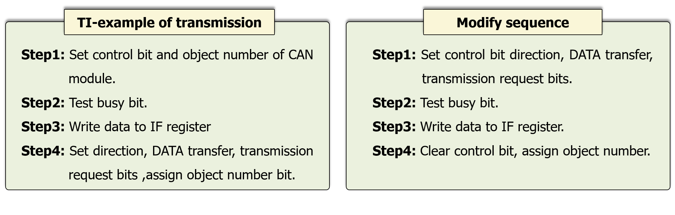
3. IFxMask usage
3.1 The ID MCU gets is to "AND" the mask content
3.2 Any bit in 0 is "don't care" (TRM seems to indicate this....)
Which one is correct?
In the user's testing, the ID is 0x030 (11 bits). Its IFxARB is 0x80C0 0000. The corresponding IFxMask is set 0x40C0 0000(0x030), but the user found the data could not be received. But when it was changed to 0x40DC 0000 (0x037->0x030~0x037), then the data could be received.
Therefore, it seems 3.1 is correct usage.
Do you have any comment?
4. Are the upper 16-bit and lower 16 bit of CAN registers are not continuous/back-to-back?
For example, for IFxCMD's lower 16bit is at 100h, but upper 16bit seems in 102h rather than 101h??
Is this what "21.3 Address/Data Bus Bridge" of TRM says?
Would you please help confirm?
Wayne Huang

