This thread has been locked.

If you have a related question, please click the "Ask a related question" button in the top right corner. The newly created question will be automatically linked to this question.

TMS320F28379D: How to reduce the time beetween the CS pulse and the beginning of the CLK on SPI communication

Part Number: TMS320F28379D
Other Parts Discussed in Thread: ADS8684, ADS8684A

Hello everyone,

I am working on a project with a F28379D, I have a project with all peripherals that I need (PWM, ADC...) and I am currently designing the SPI communication to use an external ADC (ADS8684).

I designed all the function that I need and my SPI seems to be OK (I don't have the ADS8684A yet so I just look the signals of the SPI bus with an Oscilloscope).

To optimize my code I wanted to see where do I loose time calculation in the program. I did some test and the fact is that my SPI is taking a lot of time...

Here is my problem :

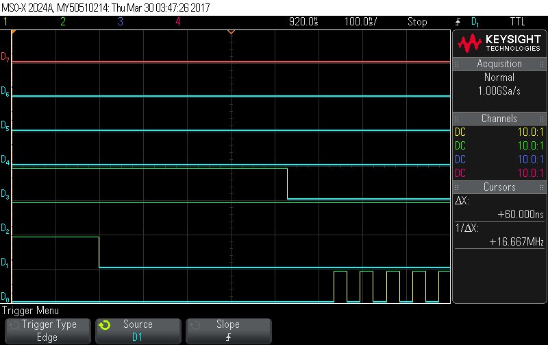
I don't understand why I have more than 500ns beetween my instruction GPIO_WRITE(32,0), and my SPI_writeData...

Here is a capture of my oscillo ( D0 is the CLK signal of the SPIA; D1 is GPIO 32; D3 is the CS signal of the SPIA)

Here is my instruction :

And here is the configuration of my SPIA :

I precise again that my SPI is connected to nothing for the moment, I don't think that's the problem but I precise it...

Thank you in advance for your answer !

Guillaume

  • Guillaume,

    You could use the disassembly window in CCS to peek at the assembly instructions being used for the GPIO and SPI write functions. From there you can determine the expected number of CPU cycles required for the functions to execute. You may be able to write your own, more efficient functions. 

    However, is there a reason why you cannot use the CS signal of the SPI directly vs. the GPIO pin? I took a quick peek at the SPI timing diagram of the ADS8684 and it seems doable. Do you have more than one ADC attached to the SPI bus?

  • Hello Gus,

    First, thank you for your answer, I never used the disassembly window so I will try to investigate this on monday.

    The TI's functions that I used "SPI_writeDataBlockingFIFI8bits" seems to already mange the CS... The GPIO that I add was juste to measure the time of the function..

    I have only one ADC.

    Guillaume

  • OK, I misread your question. The delay time between the CS pin going low to the fist SPICLK pulse is given in the device datasheet, see "SPI Master Mode Switching Characteristics (Clock Phase = 1)", timing 23 ("Delay time, SPISTE valid to SPICLK"). It looks like its approximately 2 SPI clocks (plus/minus some variance). This timing is fixed and cannot be changed.