


Other Parts Discussed in Thread: LAUNCHXL-F280049C
Hi there,
I'm having trouble with initializing the ADCs. I do the exact same thing for ADC A and ADC B and if I apply a signal all the ADCs seam to properly sample the signal except of the ADC A returns the signal with half the amplitude compared to ADC B.
Here's my init code:
    // allow adjusting registers
    EALLOW;
    // Enable internal 3.3V reference voltage
    // Enable internal reference on ADCs
    AnalogSubsysRegs.ANAREFCTL.bit.ANAREFASEL = ADC_INTERNAL;
    AnalogSubsysRegs.ANAREFCTL.bit.ANAREFA2P5SEL = ADC_VREF3P3;
    AnalogSubsysRegs.ANAREFCTL.bit.ANAREFBSEL = ADC_INTERNAL;
    AnalogSubsysRegs.ANAREFCTL.bit.ANAREFB2P5SEL = ADC_VREF3P3;

    // configure ADCCLK prescale. Max according to ds is 50MHz.
    AdcaRegs.ADCCTL2.bit.PRESCALE = 2;
    AdcbRegs.ADCCTL2.bit.PRESCALE = 2;

    // Cause the interrupt to be triggered after conversion
    AdcaRegs.ADCCTL1.bit.INTPULSEPOS = 1;
    AdcbRegs.ADCCTL1.bit.INTPULSEPOS = 1;

    AdcaRegs.ADCSOC0CTL.bit.CHSEL = 0;
    AdcaRegs.ADCSOC1CTL.bit.CHSEL = 1;
    AdcaRegs.ADCSOC2CTL.bit.CHSEL = 2;
    AdcaRegs.ADCSOC3CTL.bit.CHSEL = 3;
    AdcaRegs.ADCSOC4CTL.bit.CHSEL = 4;
    AdcaRegs.ADCSOC5CTL.bit.CHSEL = 5;
    AdcaRegs.ADCSOC6CTL.bit.CHSEL = 6;
    AdcaRegs.ADCSOC7CTL.bit.CHSEL = 7;
    AdcbRegs.ADCSOC0CTL.bit.CHSEL = 0;
    AdcbRegs.ADCSOC1CTL.bit.CHSEL = 1;
    AdcbRegs.ADCSOC2CTL.bit.CHSEL = 2;
    AdcbRegs.ADCSOC3CTL.bit.CHSEL = 3;
    AdcbRegs.ADCSOC4CTL.bit.CHSEL = 4;
    AdcbRegs.ADCSOC5CTL.bit.CHSEL = 5;
    AdcbRegs.ADCSOC6CTL.bit.CHSEL = 6;
    AdcbRegs.ADCSOC7CTL.bit.CHSEL = 7;
    // Setup acquisition windows for ADC A and B and all required SOCs
    // (register holds value - 1)
    uint16_t u16Acqps = 24;
    AdcaRegs.ADCSOC0CTL.bit.ACQPS = u16Acqps -1;
    AdcaRegs.ADCSOC1CTL.bit.ACQPS = u16Acqps -1;
    AdcaRegs.ADCSOC2CTL.bit.ACQPS = u16Acqps -1;
    AdcaRegs.ADCSOC3CTL.bit.ACQPS = u16Acqps -1;
    AdcaRegs.ADCSOC4CTL.bit.ACQPS = u16Acqps -1;
    AdcaRegs.ADCSOC5CTL.bit.ACQPS = u16Acqps -1;
    AdcaRegs.ADCSOC6CTL.bit.ACQPS = u16Acqps -1;
    AdcaRegs.ADCSOC7CTL.bit.ACQPS = u16Acqps -1;
    AdcbRegs.ADCSOC0CTL.bit.ACQPS = u16Acqps -1;
    AdcbRegs.ADCSOC1CTL.bit.ACQPS = u16Acqps -1;
    AdcbRegs.ADCSOC2CTL.bit.ACQPS = u16Acqps -1;
    AdcbRegs.ADCSOC3CTL.bit.ACQPS = u16Acqps -1;
    AdcbRegs.ADCSOC4CTL.bit.ACQPS = u16Acqps -1;
    AdcbRegs.ADCSOC5CTL.bit.ACQPS = u16Acqps -1;
    AdcbRegs.ADCSOC6CTL.bit.ACQPS = u16Acqps -1;
    AdcbRegs.ADCSOC7CTL.bit.ACQPS = u16Acqps -1;

    // set all SOCs  to trigger on ePWM1 SOCA. Since no further
    // priorization is taking place the SOCs will be triggered in a
    // round robbing manner
    AdcaRegs.ADCSOC0CTL.bit.TRIGSEL = 5;
    AdcaRegs.ADCSOC1CTL.bit.TRIGSEL = 5;
    AdcaRegs.ADCSOC2CTL.bit.TRIGSEL = 5;
    AdcaRegs.ADCSOC3CTL.bit.TRIGSEL = 5;
    AdcaRegs.ADCSOC4CTL.bit.TRIGSEL = 5;
    AdcaRegs.ADCSOC5CTL.bit.TRIGSEL = 5;
    AdcaRegs.ADCSOC6CTL.bit.TRIGSEL = 5;
    AdcaRegs.ADCSOC7CTL.bit.TRIGSEL = 5;
    AdcbRegs.ADCSOC0CTL.bit.TRIGSEL = 5;
    AdcbRegs.ADCSOC1CTL.bit.TRIGSEL = 5;
    AdcbRegs.ADCSOC2CTL.bit.TRIGSEL = 5;
    AdcbRegs.ADCSOC3CTL.bit.TRIGSEL = 5;
    AdcbRegs.ADCSOC4CTL.bit.TRIGSEL = 5;
    AdcbRegs.ADCSOC5CTL.bit.TRIGSEL = 5;
    AdcbRegs.ADCSOC6CTL.bit.TRIGSEL = 5;
    AdcbRegs.ADCSOC7CTL.bit.TRIGSEL = 5;

    // Cause interrupt once SOC7 of ADC A is done
    AdcaRegs.ADCINTSEL1N2.bit.INT1SEL = 7;
    AdcaRegs.ADCINTSEL1N2.bit.INT1E = 1; // Enable INT1 flag
    AdcaRegs.ADCINTFLGCLR.bit.ADCINT1 = 1; // Make sure INT1 flag is cleared
    AdcbRegs.ADCINTSEL1N2.bit.INT1SEL = 7;
    AdcbRegs.ADCINTSEL1N2.bit.INT1E = 1; // Enable INT1 flag
    AdcbRegs.ADCINTFLGCLR.bit.ADCINT1 = 1; // Make sure INT1 flag is cleared

    // Function for ADC-A interrupt 1. Since ADC-B is setup
    // identically to ADCA it should be done at the same time.
    PieVectTable.ADCA1_INT = &etgadc_A1ISR;

    // Power up the ADC
    AdcaRegs.ADCCTL1.bit.ADCPWDNZ = 1;
    AdcbRegs.ADCCTL1.bit.ADCPWDNZ = 1;
    // stop to allow register changes
    EDIS;
And the graph of the results:
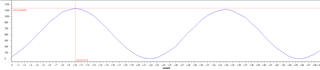
Above: ADC_A
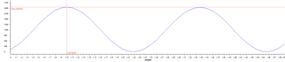
Above: ADC_B
Am I missing some setting that remains on default and therefore causes the issue? Any help would be highly appreciated.
Thanks!

