This thread has been locked.

If you have a related question, please click the "Ask a related question" button in the top right corner. The newly created question will be automatically linked to this question.

TMS320F280049: Can I use PGA_GND as ADC input?

Part Number: TMS320F280049


Hi,

since we don't need PGA and the ADC pin is not enough for my system, can I use PGA_GND as ADC input, such as the route below:

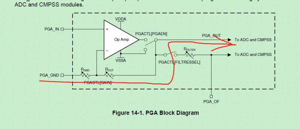
For example. PGA1_OUT is connected to A11 and B7, PGA1_OUT and PGA_GND is connected by resistor as shown in the picture above.

Can I use A11 to sense PGA_GND signal.

  • Hi Howard,

    No, this is not supported / possible.

  • Cottier,

    could you please tell me why it's not possible?

  • Hi Howard,

    The PGA ground is a ground pin with allowable input range of -50mV to +200mV as specified by the datasheet.  Higher voltages will cause improper internal biasing of the device. 

    These resistors are also ~20kohm, so it would not be possible to set the S+H long enough to allow for adequate setting and it is not possible to add a charge-sharing capacitor after the resistors to operate the ADC input in a charge-sharing configuration.   In any case, I'm not sure that you'll even get a path through if the PGA isn't enabled.  

    Any reason the customer isn't using the PGA input in this case?  The PGA input path is buffered and has higher dynamic range due to selectable gains.  Worst-case, the customer can add a voltage divider to scale down the input, then gain it back up with the PGA.  

  • The min gain of PGA is 3, not 1, so  the max signal can not over 1.1V, this limit our sample gain circuit.

    if we scale down our sample to 1/3 and sent to PGA to use 3 gain, is there some signal lost?

  • Hi '1701,

    The PGA isn't fully rail-to-rail (see the "PGA Output Range" specification in the datasheet) so you lose 350mV of range from the VSSA and VDDA.  This may not really be a problem on the high side depending on the selected VREFHI (e.g. 2.5V will be much below VDDA - 0.35V).  On the low side, you can circumvent this by adding some positive offset when you scale the signal. 

    You'll also see some additional error from the gain and offset error of the PGA (see the datasheet specifications for the PGA).  This is similar to additional error you'd get from component tolerances in your external signal conditioning circuits. 

    On the plus side, the PGA inputs are buffered, so ideally you'd use these for channels that would otherwise need an op-amp due to high impedance (e.g. a voltage divider with large R values) which can reduce the cost of external components in the system.  

  • Devin,

    so the idea we integrate PGA is to be used to measure signal with high output impedance, right?

  • Hi Howard,

    Yes, you'll get the maximum value out of the PGA by using it for signals with high impedance that would otherwise need an op-amp to correctly drive the ADC. 

    The other high value-added use case would be a channel that you want to sense at multiple ranges.  For instance, if you have a current to be sensed that has a wide range of values, you could use two (or more) different sensing paths with different gains.  This would require multiple ADC input pins and multiple sets of signal conditioning circuits (or an external PGA).  Instead, with the PGA, you would use a single input (the PGA input) and then change the gain based on the level of the current: when the current is very small, a large gain is used to provide better resolution, and when the current is large, a smaller gain is used so that the sensed value doesn't saturate. 

    But you can also use the PGA for an arbitrary analog input as long as you can set the input range to work with one of the PGA gain settings.