


1. The chip model used:(使用的芯片型号:)
2、purpose(目的):
想要给这个芯片外接一个SDRAM的存储器。
3、problem(存在的问题):
(1)DSP的GPIO_72引脚被Boot Mode Selection Switch占用了
此时外扩的SDRAM的数据位D12也是需要接到GPIO72上的。
The GPIO_72 pin of the DSP is occupied by the Boot Mode Selection Switch.
At this time, the data bit D12 of the expanded SDRAM also needs to be connected to GPIO72.
(2)DSP的GPIO_44引脚被ethernet的引脚占用了
此时外扩的SDRAM的地址位A4也是需要接到GPIO44上的。
The GPIO_44 pin of the DSP is occupied by the pin of the ethernet.
At this time, the address bit A4 of the expanded SDRAM also needs to be connected to GPIO44.
(3)DSP的GPIO_75引脚被ethernet的引脚占用了
此时外扩的SDRAM的数据位D9也是需要接到GPIO75上的。
The GPIO_75 pin of the DSP is occupied by the pin of the ethernet.
At this time, the data bit D9 of the expanded SDRAM also needs to be connected to GPIO75.
4、Try a solution(尝试解决方法):
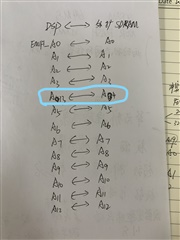
尝试1:(只修改冲突的地址线和数据线)
将外扩的SDRAM冲突的地址线A4连接到EMIF1_A13上(不按照原来的SDRAM_A4连接到EMIF1_A4)
将外扩的SDRAM冲突的数据线D9、D12对应连接到EMIF1的D16和D17上(不按照原来的SDRAM_D9、D12连接到EMIF1_D9、D12)
Attempt 1: (Only modify the conflicting address line and data line)
Connect the externally expanded SDRAM conflicting address line A4 to EMIF1_A13 (not connect to EMIF1_A4 according to the original SDRAM_A4).
Connect the conflicting data lines D9 and D12 of the externally expanded SDRAM to D16 and D17 of EMIF1 (not connected to EMIF1_D9 and D12 according to the original SDRAM_D9 and D12).
连接方式如下图:
The connection method is as follows:

尝试2:(将SDRAM的地址线和数据线整体平移连接到DSP的EMIF1上)
将外扩的SDRAM的地址线A0-A12连接到EMIF1_A5-A17上
将外扩的SDRAM的数据线D0-D15连接到EMIF1_D16-D31上
Attempt 2: (Connect the address line and data line of the SDRAM to the EMIF1 of the DSP as a whole in translation)
Connect the address lines A0-A12 of the externally expanded SDRAM to EMIF1_A5-A17
Connect the data lines D0-D15 of the externally expanded SDRAM to EMIF1_D16-D31


5、Questions to ask(请教的问题)
上述两种尝试的连接方式,如果选择第一种尝试方式,(只修改冲突的地址线和数据线),不修改其他的地址线和数据线。
如下图的这种连接方式:
If you choose the first connection method for the above two attempts, (only modify the conflicting address line and data line), do not modify the other address lines and data lines.
This connection method as shown in the figure below:
这种连接方式,地址线和数据线不是对应连接的,在CCS端进行程序驱动的时候,也是方便的吧,只需要硬件上连接之后,代码里面修改一下引脚,如下图所示,修改成注释的样子:
In this connection method, the address line and the data line are not correspondingly connected. It is also convenient when the program is driven on the CCS side. You only need to modify the pins in the code after the hardware is connected, as shown in the figure below. The annotation looks like:

按照这样修改,是否符合DSP的外扩连接的标准?是否影响SDRAM的正常使用呢?
According to this modification, does it comply with the DSP's external expansion connection standard? Does it affect the normal use of SDRAM?
6、 The reasons for choosing Attempt 1 are(选用尝试1的原因是):
方便PCB图的修改。
It is convenient to modify the PCB diagram.
7、 What is your suggestion for modification?(请教一下,您的修改建议是?)
I'm here to ask!
thanks!
特来请教!
感谢!
