


Other Parts Discussed in Thread: C2000WARE
Hi,
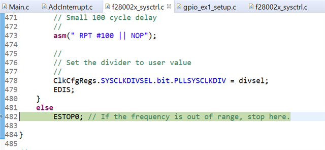
we have configured the clock source as INT_OSC2, and main CPU frequency to be 100MHz, but the program will stop in the place below:
after I click resume, it will work correctly.
The system configuration code is as below, could you please tell what's wrong here?
//###########################################################################
//
// FILE:   f28002x_sysctrl.c
//
// TITLE:  f28002x Device System Control Initialization & Support Functions.
//
// DESCRIPTION:  Example initialization of system resources.
//
//###########################################################################
// $TI Release: F28002x Support Library v3.04.00.00 $
// $Release Date: Fri Feb 12 18:58:34 IST 2021 $
// $Copyright:
// Copyright (C) 2021 Texas Instruments Incorporated - http://www.ti.com/
//
// Redistribution and use in source and binary forms, with or without
// modification, are permitted provided that the following conditions
// are met:
//
//   Redistributions of source code must retain the above copyright
//   notice, this list of conditions and the following disclaimer.
//
//   Redistributions in binary form must reproduce the above copyright
//   notice, this list of conditions and the following disclaimer in the
//   documentation and/or other materials provided with the
//   distribution.
//
//   Neither the name of Texas Instruments Incorporated nor the names of
//   its contributors may be used to endorse or promote products derived
//   from this software without specific prior written permission.
//
// THIS SOFTWARE IS PROVIDED BY THE COPYRIGHT HOLDERS AND CONTRIBUTORS
// "AS IS" AND ANY EXPRESS OR IMPLIED WARRANTIES, INCLUDING, BUT NOT
// LIMITED TO, THE IMPLIED WARRANTIES OF MERCHANTABILITY AND FITNESS FOR
// A PARTICULAR PURPOSE ARE DISCLAIMED. IN NO EVENT SHALL THE COPYRIGHT
// OWNER OR CONTRIBUTORS BE LIABLE FOR ANY DIRECT, INDIRECT, INCIDENTAL,
// SPECIAL, EXEMPLARY, OR CONSEQUENTIAL DAMAGES (INCLUDING, BUT NOT
// LIMITED TO, PROCUREMENT OF SUBSTITUTE GOODS OR SERVICES; LOSS OF USE,
// DATA, OR PROFITS; OR BUSINESS INTERRUPTION) HOWEVER CAUSED AND ON ANY
// THEORY OF LIABILITY, WHETHER IN CONTRACT, STRICT LIABILITY, OR TORT
// (INCLUDING NEGLIGENCE OR OTHERWISE) ARISING IN ANY WAY OUT OF THE USE
// OF THIS SOFTWARE, EVEN IF ADVISED OF THE POSSIBILITY OF SUCH DAMAGE.
// $
//###########################################################################

//
// Included Files
//
#include "f28002x_device.h"     // Headerfile Include File
#include "f28002x_examples.h"   // Examples Include File

//
// Functions that will be run from RAM need to be assigned to a different
// section.  This section will then be mapped to a load and run address using
// the linker cmd file.
//
//      *IMPORTANT*
//
//  IF RUNNING FROM FLASH, PLEASE COPY OVER THE SECTION ".TI.ramfunc" FROM
//  FLASH TO RAM PRIOR TO CALLING InitSysCtrl(). THIS PREVENTS THE MCU FROM
//  THROWING AN EXCEPTION WHEN A CALL TO DELAY_US() IS MADE.
//
#pragma CODE_SECTION(InitFlash, ".TI.ramfunc");
#pragma CODE_SECTION(FlashOff, ".TI.ramfunc");


// The following values are used to validate PLL Frequency using DCC
//
#define   DCC_COUNTER0_TOLERANCE   1

//
// Macro used for adding delay between 2 consecutive writes to CLKSRCCTL1
// register.
// Delay = 300 NOPs
//
#define SYSCTRL_CLKSRCCTL1_DELAY  asm(" RPT #250 || NOP \n RPT #50 || NOP")

//
// InitSysCtrl - Initialization of system resources.
//
void InitSysCtrl(void)
{

    // Disable the watchdog
    DisableDog();

    //
    // Call Device_cal function when run using debugger
    // This function is called as part of the Boot code. The function is called
    // in the InitSysCtrl function since during debug time resets, the boot code
    // will not be executed and the gel script will reinitialize all the
    // registers and the calibrated values will be lost.
    //
    EALLOW;
    CpuSysRegs.PCLKCR13.bit.ADC_A = 1; // Enable ADC peripheral clock
    CpuSysRegs.PCLKCR13.bit.ADC_C = 1;
    (*Device_cal)();
    CpuSysRegs.PCLKCR13.bit.ADC_A = 0; // Return ADC clock to original state
    CpuSysRegs.PCLKCR13.bit.ADC_C = 0;
    EDIS;


    // Initialize the SYSPLL control  to generate a 200Mhz clock
    //
    // Defined options to be passed as arguments to this function are defined
    // in f2838x_examples.h.
    //
    // Note: The internal oscillator CANNOT be used as the PLL source if the
    // PLLSYSCLK is configured to frequencies above 194 MHz.
    //
    //  PLLSYSCLK = (XTAL_OSC) * (IMULT) /(REFDIV) * (ODIV) * (PLLSYSCLKDIV)
    //
    InitSysPll(INT_OSC2, IMULT_30, REFDIV_1, ODIV_3, PLLCLK_BY_1, SYSCTL_DCC_BASE0); //ʹ���ڲ�����

    // Initialize the peripheral clocks
    InitPeripheralClocks();

}

//
// InitPeripheralClocks - Initializes the clocks for the peripherals.
//
// Note: In order to reduce power consumption, turn off the clocks to any
// peripheral that is not specified for your part-number or is not used in the
// application
//
void InitPeripheralClocks(void)
{
    EALLOW;

    CpuSysRegs.PCLKCR0.bit.DMA = 1;
    CpuSysRegs.PCLKCR0.bit.CPUTIMER0 = 1;
    CpuSysRegs.PCLKCR0.bit.TBCLKSYNC = 1;
    CpuSysRegs.PCLKCR0.bit.CPUBGCRC = 1;

    CpuSysRegs.PCLKCR2.bit.EPWM1 = 1;
    CpuSysRegs.PCLKCR2.bit.EPWM2 = 1;
    CpuSysRegs.PCLKCR2.bit.EPWM6 = 1;

    CpuSysRegs.PCLKCR10.bit.CAN_A = 1;

    CpuSysRegs.PCLKCR13.bit.ADC_A = 1;
    CpuSysRegs.PCLKCR13.bit.ADC_C = 1;

    CpuSysRegs.PCLKCR14.bit.CMPSS1 = 1;
    CpuSysRegs.PCLKCR14.bit.CMPSS2 = 1;
    CpuSysRegs.PCLKCR14.bit.CMPSS3 = 1;
    CpuSysRegs.PCLKCR14.bit.CMPSS4 = 1;

    EDIS;
}

//
// DisablePeripheralClocks - Gates-off all peripheral clocks.
//
void DisablePeripheralClocks(void)
{
    EALLOW;

    CpuSysRegs.PCLKCR0.all = 0;
    CpuSysRegs.PCLKCR2.all = 0;
    CpuSysRegs.PCLKCR3.all = 0;
    CpuSysRegs.PCLKCR4.all = 0;
    CpuSysRegs.PCLKCR7.all = 0;
    CpuSysRegs.PCLKCR8.all = 0;
    CpuSysRegs.PCLKCR9.all = 0;
    CpuSysRegs.PCLKCR10.all = 0;
    CpuSysRegs.PCLKCR13.all = 0;
    CpuSysRegs.PCLKCR14.all = 0;
    CpuSysRegs.PCLKCR19.all = 0;
    CpuSysRegs.PCLKCR20.all = 0;
    CpuSysRegs.PCLKCR21.all = 0;

    EDIS;
}

//
// InitFlash - This function initializes the Flash Control registers.
//
//      *CAUTION*
// This function MUST be executed out of RAM. Executing it out of OTP/Flash
// will yield unpredictable results.
//
#ifdef __cplusplus
#pragma CODE_SECTION(".TI.ramfunc");
#endif
void InitFlash(void)
{
    EALLOW;

    //
    // At reset bank and pump are in sleep. A Flash access will power up the
    // bank and pump automatically.
    //
    // Power up Flash bank and pump. This also sets the fall back mode of
    // flash and pump as active.
    //
    Flash0CtrlRegs.FPAC1.bit.PMPPWR = 0x1;
    Flash0CtrlRegs.FBFALLBACK.bit.BNKPWR0 = 0x3;

    //
    // Disable Cache and prefetch mechanism before changing wait states
    //
    Flash0CtrlRegs.FRD_INTF_CTRL.bit.DATA_CACHE_EN = 0;
    Flash0CtrlRegs.FRD_INTF_CTRL.bit.PREFETCH_EN = 0;

    //
    // Set waitstates according to frequency
    //
    //      *CAUTION*
    // Minimum waitstates required for the flash operating at a given CPU rate
    // must be characterized by TI. Refer to the datasheet for the latest
    // information.
    //
#if CPU_FRQ_100MHZ
        Flash0CtrlRegs.FRDCNTL.bit.RWAIT = 0x4;
#endif

    //
    // Enable Cache and prefetch mechanism to improve performance of code
    // executed from Flash.
    //
    Flash0CtrlRegs.FRD_INTF_CTRL.bit.DATA_CACHE_EN = 1;
    Flash0CtrlRegs.FRD_INTF_CTRL.bit.PREFETCH_EN = 1;

    //
    // At reset, ECC is enabled. If it is disabled by application software and
    // if application again wants to enable ECC.
    //
    Flash0EccRegs.ECC_ENABLE.bit.ENABLE = 0xA;

    EDIS;

    //
    // Force a pipeline flush to ensure that the write to the last register
    // configured occurs before returning.
    //
    __asm(" RPT #7 || NOP");
}

//
// FlashOff - This function powers down the flash
//
//      *CAUTION*
// This function MUST be executed out of RAM. Executing it out of OTP/Flash
// will yield unpredictable results. Also you must seize the flash pump in
// order to power it down.
//
#ifdef __cplusplus
#pragma CODE_SECTION(".TI.ramfunc");
#endif
void FlashOff(void)
{
    EALLOW;

    //
    // Power down bank
    //
    Flash0CtrlRegs.FBFALLBACK.bit.BNKPWR0 = 0;

    //
    // Power down pump
    //
    Flash0CtrlRegs.FPAC1.bit.PMPPWR = 0;

    EDIS;
}


//
// ServiceDog - This function resets the watchdog timer.
//
// Enable this function for using ServiceDog in the application.
//
void ServiceDog(void)
{
    EALLOW;
    WdRegs.WDKEY.bit.WDKEY = 0x0055;
    WdRegs.WDKEY.bit.WDKEY = 0x00AA;
    EDIS;
}

//
// DisableDog - This function disables the watchdog timer.
//
void DisableDog(void)
{
    volatile Uint16 temp;

    //
    // Grab the clock config first so we don't clobber it
    //
    EALLOW;
    temp = WdRegs.WDCR.all & 0x0007;
    WdRegs.WDCR.all = 0x0068 | temp;
    EDIS;
}

//---------------------------------------------------------------------------
// Example: EnableDog:
//---------------------------------------------------------------------------
// This function enables the watchdog timer.
#pragma CODE_SECTION(EnableDog, ".TI.ramfunc");
void EnableDog(void)
{
    EALLOW;
    WdRegs.WDCR.all= 0x002E;
    EDIS;
}

//
// InitPll - This function initializes the PLL registers.
//
// Note: This function uses the DCC to check that the PLLRAWCLK is running at
// the expected rate. The desirable DCC can be provided as a parameter.
//
void InitSysPll(Uint16 clock_source, Uint16 imult, Uint32 refdiv, Uint32 odiv,
                 Uint16 divsel, Uint32 dccbase)
{
    Uint32 timeout,temp_syspllmult, pllLockStatus;
    bool status;

    if(((clock_source & 0x3) == ClkCfgRegs.CLKSRCCTL1.bit.OSCCLKSRCSEL)    &&
       (((clock_source & 0x4) >> 2) == ClkCfgRegs.XTALCR.bit.SE)           &&
       (imult  == ClkCfgRegs.SYSPLLMULT.bit.IMULT)           &&
       (refdiv  == ClkCfgRegs.SYSPLLMULT.bit.REFDIV)          &&
       (odiv == ClkCfgRegs.SYSPLLMULT.bit.ODIV)               &&
       (divsel == ClkCfgRegs.SYSCLKDIVSEL.bit.PLLSYSCLKDIV))
    {
        //
        // Everything is set as required, so just return
        //
        return;
    }

    EALLOW;

    //
    // First modify the PLL multipliers if the multipliers need an update or PLL needs
    // to be powered on / enabled
    //
    if((imult != ClkCfgRegs.SYSPLLMULT.bit.IMULT) ||
       (refdiv != ClkCfgRegs.SYSPLLMULT.bit.REFDIV)||
       (odiv != ClkCfgRegs.SYSPLLMULT.bit.ODIV) ||
       (1U != ClkCfgRegs.SYSPLLCTL1.bit.PLLEN))
    {
        //
        // Bypass PLL and set dividers to /1
        //
        ClkCfgRegs.SYSPLLCTL1.bit.PLLCLKEN = 0;

        //
        // Delay of at least 120 OSCCLK cycles required post PLL bypass
        //
        asm(" RPT #120 || NOP");

        //
        // Evaluate PLL multipliers and dividers
        //
        temp_syspllmult = ((refdiv << 24U) | (odiv << 16U)| imult);

        //
        // Turnoff the PLL
        //
        ClkCfgRegs.SYSPLLCTL1.bit.PLLEN = 0;
        EDIS;

        //
        // Delay of at least 66 OSCCLK cycles
        //
        asm(" RPT #66 || NOP");

        if(((clock_source & 0x3) != ClkCfgRegs.CLKSRCCTL1.bit.OSCCLKSRCSEL) ||
          (((clock_source & 0x4) >> 2) != ClkCfgRegs.XTALCR.bit.SE))
        {
            switch (clock_source)
            {
                case INT_OSC1:
                    SysIntOsc1Sel();
                    break;

                case INT_OSC2:
                    SysIntOsc2Sel();
                    break;

                case XTAL_OSC:
                    SysXtalOscSel();
                    break;

                case XTAL_OSC_SE:
                    SysXtalOscSESel();
                    break;
            }
        }

        //
        // Delay of at least 60 OSCCLK cycles
        //
        asm(" RPT #60 || NOP");

        EALLOW;

        //
        // Set dividers to /1 to ensure the fastest PLL configuration
        //
        ClkCfgRegs.SYSCLKDIVSEL.bit.PLLSYSCLKDIV = 0;

        //
        // Program PLL multipliers
        //
        ClkCfgRegs.SYSPLLMULT.all = temp_syspllmult;

        //
        // Enable SYSPLL
        //
        ClkCfgRegs.SYSPLLCTL1.bit.PLLEN = 1;

        //
        // Lock time is 1024 OSCCLK * (REFDIV+1)
        //
        timeout = (1024U * (refdiv + 1U));
        pllLockStatus = ClkCfgRegs.SYSPLLSTS.bit.LOCKS;

        //
        // Wait for the SYSPLL lock
        //
        while((pllLockStatus != 1) && (timeout != 0U))
        {
            pllLockStatus = ClkCfgRegs.SYSPLLSTS.bit.LOCKS;
            timeout--;
        }

        EDIS;

        //
        // Check PLL Frequency using DCC
        //
        status = IsPLLValid(dccbase, clock_source, INT_PLL_SYSPLL,
                            imult, odiv , refdiv);

    }
    else
    {
        //
        // Re-Lock of PLL not needed since the multipliers
        // are not updated
        //
        status = true;
    }

    if(status)
    {
        EALLOW;
        //
        // Set divider to produce slower output frequency to limit current increase
        //
        if(divsel != PLLCLK_BY_126)
        {
            ClkCfgRegs.SYSCLKDIVSEL.bit.PLLSYSCLKDIV = divsel + 1;
        }
        else
        {
            ClkCfgRegs.SYSCLKDIVSEL.bit.PLLSYSCLKDIV = divsel;
        }

        //
        // Enable PLLSYSCLK is fed from system PLL clock
        //
        ClkCfgRegs.SYSPLLCTL1.bit.PLLCLKEN = 1;

        //
        // Small 100 cycle delay
        //
        asm(" RPT #100 || NOP");

        //
        // Set the divider to user value
        //
        ClkCfgRegs.SYSCLKDIVSEL.bit.PLLSYSCLKDIV = divsel;
        EDIS;
    }
    else
        ESTOP0; // If the frequency is out of range, stop here.

}

//
// SysIntOsc1Sel - This function switches to Internal Oscillator 1.
//
void SysIntOsc1Sel(void)
{
    EALLOW;
    ClkCfgRegs.CLKSRCCTL1.bit.OSCCLKSRCSEL = 2;     // Clk Src = INTOSC1
    EDIS;
}

//
// SysIntOsc2Sel - This function switches to Internal oscillator 2.
//
void SysIntOsc2Sel(void)
{
    EALLOW;
    ClkCfgRegs.CLKSRCCTL1.bit.OSCCLKSRCSEL = 0;     // Clk Src = INTOSC2
    EDIS;
}

//
// PollX1Counter - Clear the X1CNT counter and then wait for it to saturate
// four times.
//
static void
PollX1Counter(void)
{
    Uint16 loopCount = 0;

    //
    // Delay for 1 ms while the XTAL powers up
    //
    // 2000 loops, 5 cycles per loop + 9 cycles overhead = 10009 cycles
    //
    F28x_usDelay(2000);

    //
    // Clear and saturate X1CNT 4 times to guarantee operation
    //
    do
    {
        //
        // Keep clearing the counter until it is no longer saturated
        //
        while(ClkCfgRegs.X1CNT.all > 0x1FF)
        {
            ClkCfgRegs.X1CNT.bit.CLR = 1;
            ClkCfgRegs.X1CNT.bit.CLR = 0;
        }

        //
        // Wait for the X1 clock to saturate
        //
        while(ClkCfgRegs.X1CNT.all != 0x7FFU)
        {
            ;
        }

        //
        // Increment the counter
        //
        loopCount++;
    }while(loopCount < 4);
}
// SysXtalOscSel - This function switches to External CRYSTAL oscillator.
//
void SysXtalOscSel(void)
{
    EALLOW;
    ClkCfgRegs.XTALCR.bit.OSCOFF = 0;     // Turn on XTALOSC
    ClkCfgRegs.XTALCR.bit.SE = 0;         // Select crystal mode
    EDIS;

    //
    // Wait for the X1 clock to saturate
    //
    PollX1Counter();

    //
    // Select XTAL as the oscillator source
    //
    EALLOW;
    ClkCfgRegs.CLKSRCCTL1.bit.OSCCLKSRCSEL = 1;
    EDIS;

    //
    // If a missing clock failure was detected, try waiting for the X1 counter
    // to saturate again. Consider modifying this code to add a 10ms timeout.
    //
    while(ClkCfgRegs.MCDCR.bit.MCLKSTS != 0)
    {
        EALLOW;
        ClkCfgRegs.MCDCR.bit.MCLKCLR = 1;
        EDIS;

        //
        // Wait for the X1 clock to saturate
        //
        PollX1Counter();

        //
        // Select XTAL as the oscillator source
        //
        EALLOW;
        ClkCfgRegs.CLKSRCCTL1.bit.OSCCLKSRCSEL = 1;
        EDIS;
    }
}

//
// SysXtalOscSESel - This function switches to external oscillator in
// single-ended mode and turns off all other clock sources to minimize power
// consumption. This option may not be available on all device packages
//
void
SysXtalOscSESel (void)
{
    EALLOW;
    ClkCfgRegs.XTALCR.bit.OSCOFF = 0;     // Turn on XTALOSC
    ClkCfgRegs.XTALCR.bit.SE = 1;         // Select single-ended mode
    EDIS;

    //
    // Wait for the X1 clock to saturate
    //
    PollX1Counter();

    //
    // Select XTALOSC as the oscillator source
    //
    EALLOW;
    ClkCfgRegs.CLKSRCCTL1.bit.OSCCLKSRCSEL = 1;
    EDIS;

    //
    // If missing clock detected, there is something wrong with the oscillator
    // module.
    //
    if(ClkCfgRegs.MCDCR.bit.MCLKSTS != 0)
    {
        ESTOP0;
    }
}

//
// IDLE - Enter IDLE mode
//
void
IDLE()
{
    EALLOW;
    CpuSysRegs.LPMCR.bit.LPM = LPM_IDLE;
    EDIS;
    asm(" IDLE");
}

//
// HALT - Enter HALT mode
//
void
HALT()
{
    EALLOW;
    CpuSysRegs.LPMCR.bit.LPM = LPM_HALT;
    ClkCfgRegs.SYSPLLCTL1.bit.PLLCLKEN = 0;
    ClkCfgRegs.SYSPLLCTL1.bit.PLLEN = 0;
    EDIS;
    asm(" IDLE");
}

//*****************************************************************************
//
// SysCtl_isPLLValid()
//
//*****************************************************************************
bool
IsPLLValid(Uint32 base, Uint16 oscSource, Uint16 pllclk, Uint16 imult,
           Uint16 odiv, Uint16 refdiv)
{
    float fclk1_0ratio;
    volatile struct DCC_REGS *DccRegs;

    EALLOW;

    //
    // Assigning DCC for PLL validation
    // Enable Peripheral Clock Domain PCLKCR21 for DCC
    //
    if(base == SYSCTL_DCC_BASE0)
    {
            DccRegs = &Dcc0Regs;
            CpuSysRegs.PCLKCR21.bit.DCC0 = 1;
    }
    else if(base == SYSCTL_DCC_BASE1)
    {
            DccRegs = &Dcc1Regs;
            CpuSysRegs.PCLKCR21.bit.DCC1 = 1;
    }
    else
        ESTOP0; // Invalid DCC selected

    //
    // Clear Error & Done Flag
    //
    DccRegs->DCCSTATUS.bit.ERR = 1;
    DccRegs->DCCSTATUS.bit.DONE = 1;

    //
    // Disable DCC
    //
    DccRegs->DCCGCTRL.bit.DCCENA = 0x5;

    //
    // Disable Error Signal
    //
    DccRegs->DCCGCTRL.bit.ERRENA = 0x5;

    //
    // Disable Done Signal
    //
    DccRegs->DCCGCTRL.bit.DONEENA = 0x5;

    //
    // Configure Clock Source1 to PLL
    //
    // Clk Src1 Key 0xA to enable clock source selection
    //
    switch(pllclk)
    {
        case INT_PLL_SYSPLL:
            DccRegs->DCCCLKSRC1.all = 0xA000; // Clk Src1 = SYSPLL
            break;

        default:
            //
            // Code shouldn't reach here
            //
            break;
    }

    //
    // Configure Clock Source0 to whatever is set as a reference
    // clock source for PLL
    //
    // Clk Src0 Key 0xA to enable clock source selection
    //
    switch(oscSource)
    {
        case INT_OSC1:
            DccRegs->DCCCLKSRC0.all = 0xA001; // Clk Src0 = INTOSC1
            break;

        case INT_OSC2:
            DccRegs->DCCCLKSRC0.all = 0xA002; // Clk Src0 = INTOSC2
            break;

        case XTAL_OSC:
        case XTAL_OSC_SE:
            DccRegs->DCCCLKSRC0.all = 0xA000; // Clk Src0 = XTAL
            break;

        default:
            //
            // Code shouldn't reach here
            //
            break;
    }

    //
    // Calculating frequency ratio of output clock(f1) vs reference clock(f0)
    //
    fclk1_0ratio = (float)imult / ((odiv + 1U) * (refdiv + 1));

    //
    // Computing and configuring Counter0 , Counter1 & Valid Seed Values
    // with +/-1% tolerance for the desired DCC
    //
    ComputeCntrSeedValue(base, fclk1_0ratio, DCC_COUNTER0_TOLERANCE);

    //
    // Enable Single Shot Mode
    //
    DccRegs->DCCGCTRL.bit.SINGLESHOT = 0xA;

    //
    // Enable DCC to start counting
    //
    DccRegs->DCCGCTRL.bit.DCCENA = 0xA;
    EDIS;

    //
    // Wait until Error or Done Flag is generated
    //
    while((DccRegs->DCCSTATUS.all & 3) == 0)
    {
    }

    //
    // Returns true if DCC completes without error
    //
    return((DccRegs->DCCSTATUS.all & 3) == 2);

}

//*****************************************************************************
//
// ComputeCntSeedValid - Compute Counter seed values based on the frequency ratio of output
// clock vs reference clock & tolerance expected for the desired DCC
//
//*****************************************************************************
void ComputeCntrSeedValue(Uint32 base, float fclk1_0ratio, Uint32 tolerance)
{
    Uint32 window, dccCounterSeed0, dccValidSeed0, dccCounterSeed1, total_error;
    volatile struct DCC_REGS *DccRegs;

    if(fclk1_0ratio >= 1U)
     {
        //
        // Setting Counter0 & Valid Seed Value with expected tolerance
        // Total error is 12
        //
        window = (12U * 100U) / tolerance;
        dccCounterSeed0 = window - 12U;
        dccValidSeed0 = 24U;

     }
    else
     {
        total_error = (((Uint32)2U / fclk1_0ratio) + (Uint32)10U);

        window = ((total_error * 100U)/ tolerance);

        //
        // Setting Counter0 & Valid Seed Value with expected tolerance
        //
        dccCounterSeed0 = window - total_error;
        dccValidSeed0 = (Uint32)2U * total_error;

     }

    //
    // Multiplying Counter-0 window with PLL Integer Multiplier
    //
    dccCounterSeed1 = window * fclk1_0ratio;

    //
    // Assigning DCC for PLL validation
    //
    if(base == SYSCTL_DCC_BASE0)
        DccRegs = &Dcc0Regs;
    else if(base == SYSCTL_DCC_BASE1)
        DccRegs = &Dcc1Regs;
    else
        ESTOP0; // Invalid DCC selected

    //
    // Configure COUNTER-0, COUNTER-1 & Valid Window
    //
    DccRegs->DCCCNTSEED0.bit.COUNTSEED0 = dccCounterSeed0; // Loaded Counter0 Value
    DccRegs->DCCVALIDSEED0.bit.VALIDSEED = dccValidSeed0;  // Loaded Valid Value
    DccRegs->DCCCNTSEED1.bit.COUNTSEED1 = dccCounterSeed1; // Loaded Counter1 Value
}

//
// End of File
//
The customer would like to configure through registers like in F2803x, so the example code which uses HANDLE is not friendly to them.
