This thread has been locked.

If you have a related question, please click the "Ask a related question" button in the top right corner. The newly created question will be automatically linked to this question.

TMS320F28377D: ADC returns 4096 at 2.5V instead of 3V or 3.3V

Part Number: TMS320F28377D
Other Parts Discussed in Thread: LMP7709, LMP7704, CONTROLSUITE, TINA-TI, LM358, DESIGNDRIVE

Dear Sir/Madam,

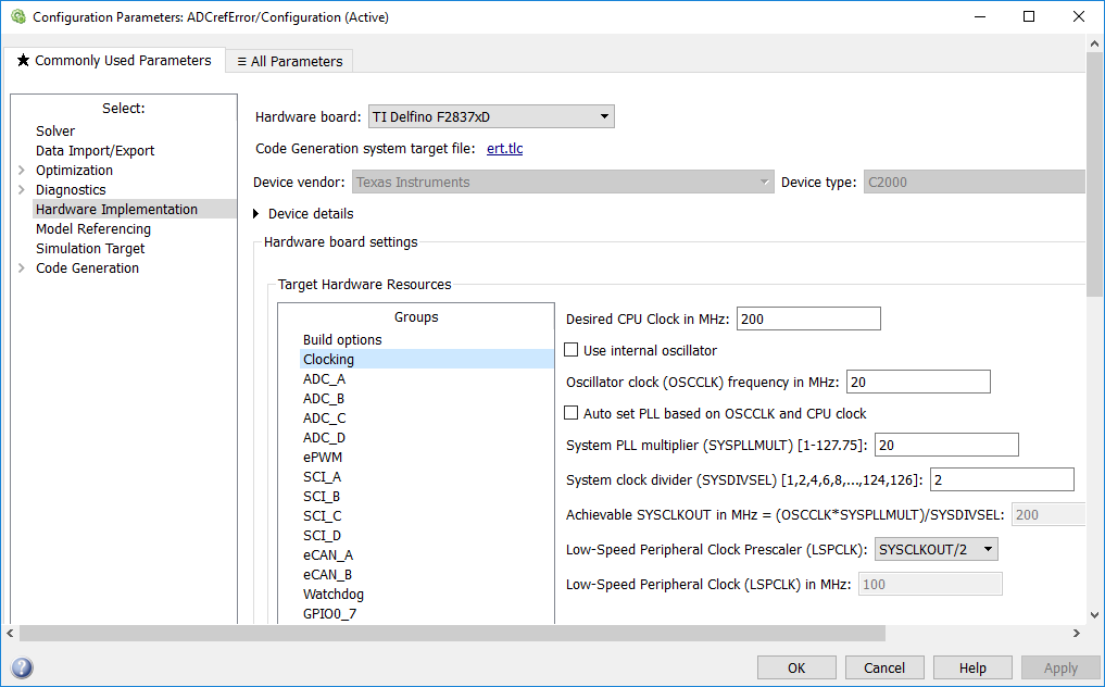
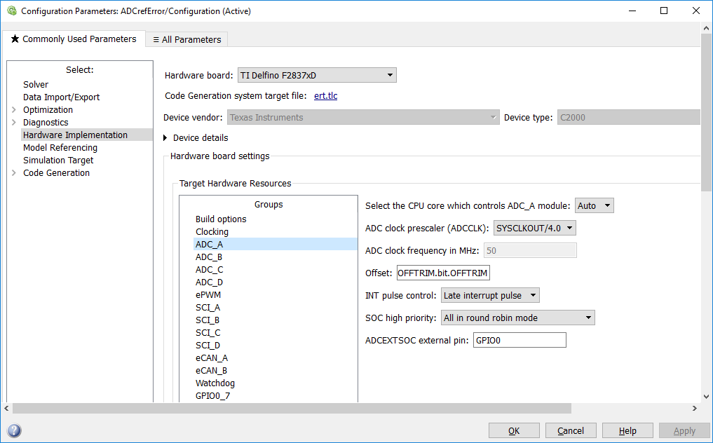
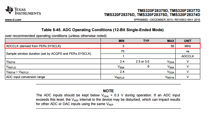
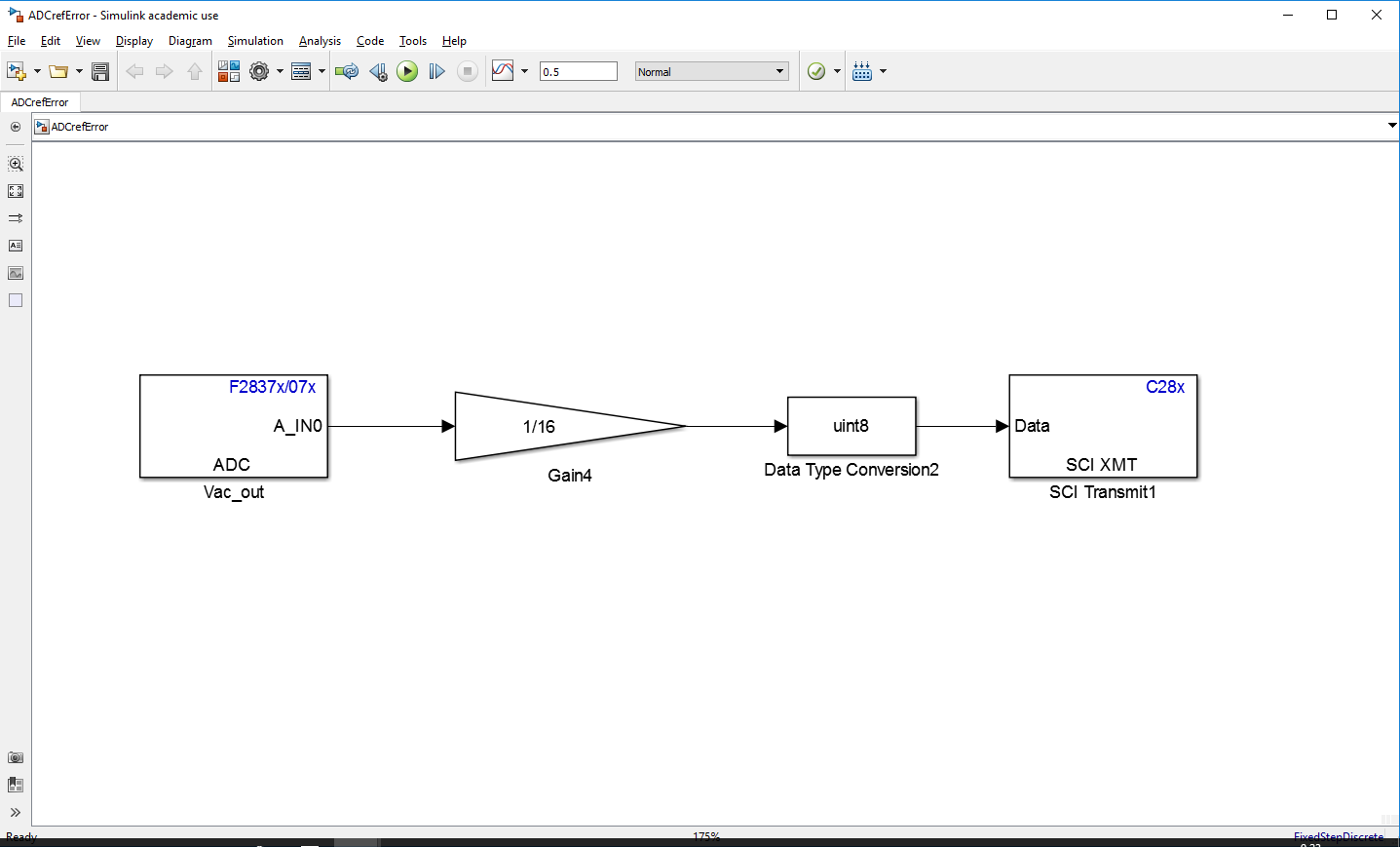
I am using Delfino TMS320F28377D controlCARD R1.1 and read a constant voltage at oone of the ADC. I have noticed that it gets "saturated" at 2.5V instead of 3V. Reading the infosheet TMDSCNCD28377D-Infosheet_v1_5.pdf, It clearly states that for my board version (R1.1), if SW2 is in the up position and SW3 is at the left position then I should get Vrefhi=3 if R42 is populated and R43 is unpopulated . This is the case wth the R42 and R43 on my board, I have measured regulator's (U13) voltage output at R42 and it is correct (3V), whereas input is 3.3V as it should. Also, I have checked ADC response with SW3 to the right position, which is supposed to give a Vrefhi of 3.3V, but I still get the same response! Both positions of SW3 make ADC saturate at approx. 2.5V. The ADC seames to work properly for Max 2.5V, because I have tested voltages at ADC input between 0 and 2.5V and I read proportional values with my code. Any ideas? I really need to read max 3V or even 3.3V in order to be able to use my analog sensors that output 0-3V.

Thank you for your time,

Panagis Vovos

Lecturer
University of Patras, Greece

  • Hi Panagis,

    Does this only occur on one ADC, or on all of them? The best place to check this would be to use the ADC input 14 or 15, which goes to all 4 ADCs. 

    Some other good places to check the reference voltage would be at the terminals of SW2 and across capacitors C15 to C18.  

    Note that there is an erratum for this ControlCard revision where the amplifiers used to drive the reference are LMP7709.  This is a decompensated op-amp, and is therefore not unity gain stable.  I wouldn't expect this to change the DC level of the ADC reference, but instead to possibly add some oscillations on top of the reference voltage, which could then show up in the ADC output.  You can try to replace this op-amp with the correct one (LMP7704) or you can try bypassing the buffers by removing the IC and wiring the inputs to the outputs.  


  • Hello Devin,

    Thank you very much for your reply. We notice the problem to all ADC channels. We have also tested C15-C18 voltages and they are all well regulated at exactly 3.0V. Therefore, Vrefhi pin is connected to 3V, indeed.

    Knowing that the Vrefhi is definetely correct we went back to programming parameters. Surprisingly, we noticed the following. With these Auto settings:

    We got nothing, but noise in our ADC (around 2800 of 4096). We realised that we had to reduce the ADC clock prescaler (ADCCLK) to /4 to measure stable voltages. It was too fast, probably. However, still 1.51V input were converted to approx. 2560/4096 and maximum remained to 2.48V.

    Magically, everything works almost fine when we also change Low-Speed Peripheral Clock Prescaler (LSPCLK) to /2. I mean 1.51V-->approx 2090 and max is 2.9V.

    Question 1) W h y  the low-speed peripheral clock prescaler has such an impact, when there is a separate ADC clock prescaler ?

                     2) Can we trim fine tune our offset (1.5V-->2048/4096) with AdcaRegs.ADCOFFTRIM.bit.OFFTRIM  and how could we possibly do that ?

    Our last working settings follows.

    Any help on those issues would be greatly appreciated.

    Thanks,

    Panagis

  • Hi Panagis,

    I would definitely recommend giving the device datasheet a thorough read; this will tell you, for example, what the maximum supported ADCCLK is:

    You may also want to look at the S+H duration you are using vs. the external impedance of your source; you can only use the minimum S+H duration with a low impedance source (R < 50 ohms, C is maybe ~10pF).

    There is no reason that LSPCLK should directly affect ADC operation.  How exactly is the ADC triggered? Is it possible that triggers are coming in through one of the communications modules (e.g. SPI) and slowing down the LSPCLK is slowing down the trigger rate?

    At mid-scale, both ADC gain and offset error will affect the conversion result. You can use the offset trim register to re-trim the ADC offset.  The procedure is documented in the device technical reference manual.  This shouldn't typically be necessary; the factory offset trim should be pretty good.  ADC gain error can't be HW trimmed by the user, but you could digitally post-process the results to scale them as needed.

    If you have offset error in your external signal specific to that ADC channel, a better strategy would be to use one of the ADC post-processing blocks (PPBs) to trim out the offset error on just that channel.

    In general, it is difficult for us to debug software issues when not using C code + code composer studio.  You may want to try running one of the provided ADC examples in ControlSUITE using CCS to definitively rule out any HW issues.  You can then work with the provider of the 3rd party tool you are using to further debug the SW.   

  • Hello again Devin,

    Thank you for your quick reply. We have been using the c2000 series for a bit less than 10 years, starting with the ezDspf2812, moving to the f28335 for something better and ending up with the f28377d control cards because of another unresolved issue by TI and a fuzzy suggestion by TI support to do so (details here). All these years we have been using the Simulink platform because we use "fast prototyping", AKA "saving power engineering researchers the coding while doing control". We have faced several issues in the past with the C2000 series, but to be honest, the control card is the biggest disapointment up to now. We have wasted about half a year porting our software from the f28355 and we are far from done, facing several other issues with Simulink, CCS or the card! By the way,  the issue with the f28355 (the reason we moved on to the f28377d control card) insists with the f28477d control card, it just costs more...

    We have read in the manual about the 50MHz limit for ADC that is why we chose /4 for the ADC clock. It makes no difference if we divide it further. If Mathworks doesn't provide proper software support for your hardware, you should just not let them say so. For example, why the clock divider for ADC is not preset to 4, but it is set to /1 and why are there the  /2 /3 options, since it doesn' t work on higher speeds anyway? People have to figure that out by reading the manual after the issue arrises?

    Never, we had a matching impedance issue with our sensors, never messed up with the prescalers in the past (f2812 or f28355) and always we use software sample time for triggering ADC. There is only an ADC block sending data to SCI-A in the code testing ADC malfunctioning. So, low-speed peripheral prescaler definetely makes no sense when affecting ADC. 

    Could you please inform us which peripherals are n the low-speed class?

    Thanks,

    Panagis

  • Hi Panagis,

    It looks like the SCI, SPI, and McBSP are all on the LSPCLK domain.  

    Are you running multiple ADCs in parallel, or just using one ADC for now?  The performance can degrade when running multiple ADCs in parallel if they aren't synchronized with respect to trigger source, resolution, and S+H duration.  How to achieve this is specified in the TRM in the section "10.3.1 Ensuring Synchronous Operation" and the performance degradation is specified in the datasheet in "ENOB" and "ADC-to-ADC isolation" specifications. It should be possible to still use software triggering and get synchronous operation, but only if an external GPIO is used for the trigger.  It does seems that the Simulink is maybe doing this per the ADCEXTSOC pin configuration?

    How much capacitance do you have on the ADC input pin?  What is the sample rate on the ADC input?  Do you see any change in the samples between the first couple samples and the steady-state if you keep periodically sampling the signal?

    I'll make sure your feedback makes it to Mathworks.

    I probably can't directly help with the 1.5 second ePWM spike issue, but if you are still seeing it on the F28377D device I can get someone else from TI to continue to debug.  

  • Hello Devin,

    Thank you again for your reply. We are using only one ADC in our example below:

    As you can see below, we use a 0.0001s sample time and no ADCINT. This is quite slow, meaning that we can get a 50hz waveform with no "voltage keeping" now that low-speed peripheral is divided by 2. But the question is, why SCI affects values read by the ADC (raises them all and saturates at 2.4V) ? In all tests,depending on the dividers settings, ADC measuring was either always good or always bad from the beginning, i.e. we didn't see values stabilizing after some time.

    Finally, the 1.5s spike issue is the reason we consider changing the boards we are using and move on to another company. So, yes, any help on unresolved issue will save us time and will give your support credit.

    Thanks again,

    Panagis

  • Hi Panagis,

    I think the issue may be that the S+H window is only set to '7'.  On this device, the S+H window is actually clocked by the SYSCLK and not the ADCCLK.  This ensures that there is never any jitter when the sample starts based on triggers coming from the CPU clock domain (and it also gives more resolution to configure the S+H window).  In any case, if SYSCLK is set to the nominal value of 200MHz and the S+H is 7 SYSCLKs, then the S+H will only be 35ns long.  The minimum S+H duration on this device is 75ns, but you may need more time depending on the characteristics of your sensor/signal source.

    We provide an input model of the ADC in the datasheet in the DS section "5.8.1.1.1 ADC Input Models".  In the TRM section "10.3.2 Choosing an Acquisition Window Duration" we provide some guidance on how to do a very rough approximation of how long the S+H window will need to be for a given signal source.  If you search through my post history on the e2e forum, I have provided some more detailed information on how to calculate the right S+H duration either analytically or by using TINA-TI (SPICE).  Of course if the sample rate is low and you don't care about the trigger-to-sample latency you can just set the S+H configuration to something large like 100 SYSCLK cycles. 

    Inadequate S+H duration would explain the signal attenuation issues. 

    I'll also let Mathworks know that they should probably change the default S+H to '15' SYSCLKs and maybe even let the user specify this in ns instead of cycles (or that they should at least note to the user that this is in SYCLKs).  

  • Hello Devin,

    Thank you very much for the info. We will study them all and define the settings for ADC. However, I do remember increasing the window to much higher values, but I did not notice any improvement, though, other settings may have been causing problems back then.
    I will get back to you with results as soon as we calculate the appropriate settings. We will start with the 100 SYSCLK cycles. Please, remember though, that we always start our measurements with a constant dc voltage, so not everything can be explained with the small window.

    The spikes are also something we are VERY interested in, so if you have any feedback on that please let me know (if there are some measurements we can add up).

    Best regards,

    Panagis
  • Dear Devin,

    We went through testing today, per your instructions. We got some very interesting results. For SOC 100 we got different measurement by some millivolts for a dc voltage, than for SOC=7. Since the input voltage is constant, a bigger SOC than 100 shouldn't alter readings further, right? Well, we increased SOC to maximum (512) and again we got different readings. We are talking about 10-20 mV between measurements for a perfectly regulated dc voltage supply, keeping voltage stable at all measurements. The differences between measurements for different SOC windows (all of them big!) does make a big deal for our high voltage sensors (600V->3V). It shouldn't make any difference for dc beyond a SOC threshold, but strangely it does. And what if we could increase SOC even further, how can we be sure that this wouldn't change our results again? Any ideas? We are kind of puzzled. 

    Another question is why didn't have such a hassle with our f28335 ADC, where the process was a 5 minutes task with defaults set???

    Thanks again,

    Panagis

  • As Devin pointed out you do have to be more careful with input stage design. Main reason is that S/H capacitor value changed from 1.64 pF in 28069 and 28335 to 14.5 pF. This is significant. Basically it means that all inputs have to be buffered, or you have to have quite big capacitor near the ADC input (preferably with low ESR and ESL).

    If you test the performance with lab bench supply and ControlCard without any buffer you can expect to come across the issues you described.

  • Hi Panagis,

    You definitely need to consider S+H duration even for DC signals; the sampling capacitor in the ADC is not guaranteed to start at any particular voltage.

    When you say your sensors go from 600V to 3V, are you using a voltage divider? The effective resistance of the voltage divider will be the parallel combination of the two resistors. You may have to balance the static power dissipation of the divider with the capability of the divider to drive the ADC. Alternately you may want to buffer the output of the divider with an op-amp.

    Mitja is correct that the ADC architecture has changed on this device from F2833x(Pipeline) to F2837x(SAR). This is partially responsible for the increase in sampling capacitance (along with supporting 16-bit operation). Note that the switch resistance of the F2837x is lower than the F2833x, but overall you need a slightly better input to drive the F2837x. You definitely won't always need an op-amp or buffer.
  • Dear Mitja and Devin,

    Thank you both for your reply. Unfortunately, all these would make sense if we did not use a buffered output for our sensor. We actually use an OP-AMP with unity gain.

    Regards,

    Panagis

  • Hi Panagis,

    Which op-amp do you use, and do you have any R-C after the op-amp output before being driven to the pin?
  • Hi Panagis,

    I am alos using simulink to debug the code.

    Did you observe great noise when you chenck the ADC results? Especially when you input a sinewave (shifte to between 0 to 3 V)? I got great noise in the ADC results. I guess we might need to solder the filters onto the experimenter kit.

    Jianwei
  • Hello Jianwei,

    I do not know about the experimenter kit. However, what I did for the control card is to set SOC to max in Simulink (that is 512) and set "Low-speed peripherals" in "clocking parameters" to /2. Anything faster than that didn't work as well. However, we use 0.0001s sample time for our model (that is quite good for any converter application=200 samples per sine cycle), so SOC=512 and L-S P clock = /2, is still much faster than the sample time.

    I hope this helps,

    Panagis

  • Hello Devin,

    Sorry for the late reply. We use the LM358 (typical choice). No, we do not have any R-C filter before being driven to the pin. This is a printed board, so I guess we shouldn't have significant paracitic elements, either. Things improve at a very, very slow ADC rate. A SOC of 512 (which is the max in Simulink) really improves things. Mind you that this is a DC voltage, so this is a long time.

    Thanks,

    Panagis

  • Hi Panagis,

    512 is also the max S+H duration supported by the HW.

    For ADCs it doesn't really matter that the input is DC; you still need to settle the ADC sampling capacitor (of unknown starting voltage) to well within your acceptable error bound.  Usually we use 1/4LSB as a conservative error limit.

    The slew rate of the LM358 is 300mV/us and the bandwidth is 700KHz.  For a 0-to-3V step (worst case starting value for the S+H capacitor), the amplifier could take as long as 3V * 90% * 1us / 0.3V = 9us to slew 90% of the range and then another  227ns * 7.4  = 1.7us to settle to 1/4LSBs = 10.7us total time. 

    Note: 300mV = (0.3/3)*4096 = 409.6 LSBs

    Note:Time constants to settle from 0.3V to 1/4LSBs = -ln(0.25 / 409.6) = 7.4 TCs

    Note: Time constant for 700KHz = 1/(2*pi*700KHz) = 227ns

    512 * 5ns = only 2.56us, so you are going to need to use a faster op-amp (or you could alternately slow the SYSCLK down significantly).  

    This calculation is only considering the op-amp itself.  The settling will probably be a little bit faster because the ADC input capacitance + PCB trace capacitance is probably less than the load specified in the LM358 datasheet (30pF for slewing and 20pF for settling).  However, this doesn't consider the interaction between the bandwidth of the op-amp and the settling time of the ADC input itself, which will be more important when the time is not dominated by the op-amp's characteristics.

    The first-order approximation of the ADC time constant is 14.5pF * 425ohms = 6.163ns.  To settle to 1/4 LSBs for a full-scale step (ignoring slewing) is -ln(.25 / 4096 ) = 9.7 time constants = 60ns. So with a perfect op-amp we could probably actually do better than the DS minimum settling time of 75ns.

    To meet the 75ns with a real op-amp, the effective TC of the op-amp + ADC input needs to be 75ns / 9.7 = 7.732ns or less.  A really rough approximation of how the time constants interact is to add them in RMS, so 7.732ns = sqrt(6.163ns^2 + xns^2) => the op amp time constant would need to be 4.67ns or less which implies the op-amp bandwith would need to be at least 1/(2*pi*4.67ns) = 34MHz.

    And here are some more approximate op-amp BWs needed to meet some S+H window durations:

    75ns => 34MHz

    100ns => 19MHz

    200ns => 8MHz

    1us => 1.5MHz

    Note that this is a pretty rough estimate, since it doesn't consider op-amp slewing, and uses a pretty rough approximation of how the op-amp interacts with the ADC input.  Best practice is to simulate the whole thing in SPICE.     

    I'd recommend that you find a pin-compatible op-amp to the LM358 with BW closer to 10MHz, sample a few from TI, and then try those in your board instead.  

  • Thanks.

    This is really helpful. The defult values in the simulink modle just did not work.

    Javy
  • Hi Devin,

    Extremely well written and quite easy to understand.

    It would be great if the text such as yours would be published in 28377 reference manual or at least in a separate document similar to "An Overview of Designing Analog Interface With TMS320F28xx 28xxx DSCs" - spraap6a already available for older devices.

    And if TI released designs would be in sync with this it would also be a big help. But instead each design has different interface. My favorite is DesignDRIVE Development Kit. Each analog input has different buffer opamp and a different RC circuit. If this was done intentionaly, then I would expect to see some comment on why they were designed in such a way. I would also expect to see some comments regarding this in the code where aquisition time is configured. But I suspect it was just copy pasted from previous designs (this is how the world runs these days)

    Best regards, Mitja

  • Hi Mitja,

    We are working on generating an application note that gives in depth guidance on how to calculate, simulate, and test for adequate S+H duration, but I don't have a definitive guideline yet for when this would be published.

    I'll look into the design drive HW and documentation.
  • Hello Devin. Thank you for your detailed reply. We will look carefully into this, replace our op-amp and get back to you with the results. Till then, we wil operated on a slower rate.

    Panagis