This thread has been locked.

If you have a related question, please click the "Ask a related question" button in the top right corner. The newly created question will be automatically linked to this question.

LAUNCHXL-F28379D: ADC input signal conditioning

Part Number: LAUNCHXL-F28379D
Other Parts Discussed in Thread: THS4531, ADS8321

Hello,

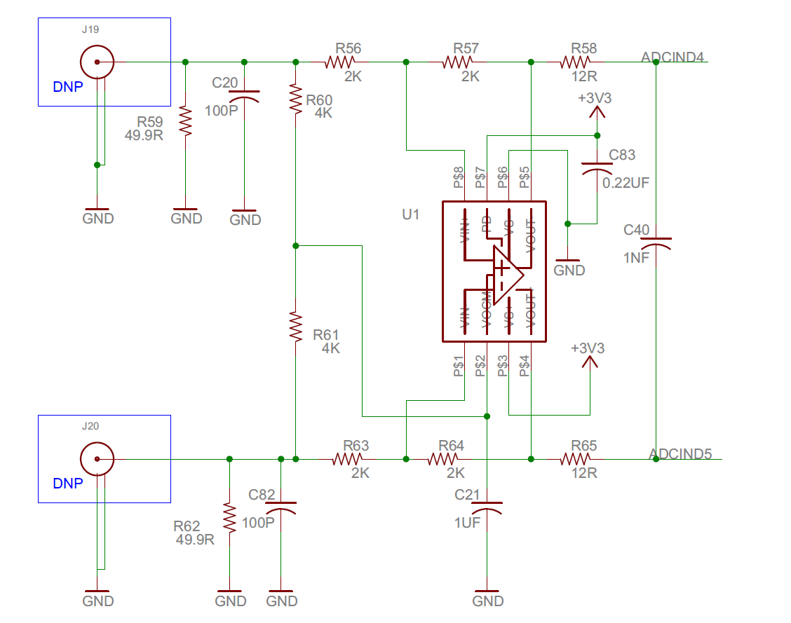
I have a couple of questions concerning the op amp circuit that is included on one of the ADC differential channels on the 28379D launch pad. I have included a snap shot of the relevant part of the circuit below. This was taken from the user guide.

My issues are:

1. The Vocm pin on the op-amp (pin 2) sets the output common mode voltage. Usually I have seen this set to half the supply, or derived from the reference voltage used by the ADC. Here it is set to the input common mode voltage. I wonder if this was intended and if so what advantage it gives. There is a precision reference source on the board, is there any reason why Vocm was not derived from that?

2.Each input has 50Ω and 100pF in parallel. This looks a bit odd to me as the resistor it gives a DC termination of 50Ω and the capacitor could cause problems to whatever is driving the input. The application notes in the data sheet for the op amp (THS4531) shows an input circuit that has the resistor and capacitor in series and this makes more sense. Is the configuration on the launch pad a mistake? If not what is the reasoning behind it?

Thanks for your help.

John Wilkes.

  • Hi John,

    (1) Yeah, I agree; this should have been connected to VREFHI/2. As-is, you will need to ensure that the common-mode of your input signal is within 50mV of VREFHI/2. It should also be possible to remove the two SMT resistors (R60 and R61) and then use wires and SMT or through-hole resistors to get this connection. The Vocm bias current is 100nA max, so you can use pretty large resistors to create the voltage divider (maybe ~10kOhm for each leg ). I would connect the input of this divider directly to the U13 voltage output. I've submitted this as feedback for the next LaunchPad revision.

    (2) It looks like the input side of this circuit was copied from the THS4531 datasheet "THS4531 and ADS8321 Test Circuit". The resistor is there to provide 50-ohm termination from your test instrument. The capacitance is, I think, just there to provide a bypass for high-frequency noise.

    On the output side, with the 1nF capacitor you should set the S+H to at least 600ns. You can use 345ns if you change the capacitor to 170pF.
  • Hi Devin,

    Thanks for your reply. For my application I will just remove R60 and R61 and not bother with trying to link the ADC reference. The THS4531 should default to half of the supply, which is 3V3, so I will lose a bit of dynamic range (10%). I can live with that for now.

    The source in my application is not 50 ohms and I’m not comfortable with that capacitor on the input so I am going to remove R59, R62, C20 and C82 as well. In fact, my source is actually single ended, so I will replace R62 with zero ohms and only populate one of the SMA connectors (J19). Hopefully that will do the trick.

    I want to sample as quickly as I can, so I will change the output capacitor as you have suggested.

    Cheers,

    John.

  • Hi Devin,

    Just to clarify: could you explain how you arrived at your acquisition times? Looking at the data sheet and the reference manual for the 28379D. I cannot see how the source capacitance affects acquisition time. This will be calculated on Rs, Ron and Ch. Given that Rs from the Launchpad circuit is 24 ohms, Ron is 700 ohms and Ch is 16.5pF. This gives an acquisition time of 148ns. Since the minimum specified for diff mode is 320ns, we have to use this. My point is, though, that the 1nF external capacitor has had no bearing on this calculation. It obviously makes a filter with Rs, but this is at 6.6MHz so shouldn’t have an impact.

    Am I missing something?

    Cheers,

    John.

  • Hi John,

    The external R and C will both affect the time needed to charge the internal S+H capacitor. You can consider the total time constant for driving the ADC to be the sequence of the driving op-amp time constant (really roughly proportional to 1 / op amp BW) + the external RC time constant + the internal RC time constant. If the op-amp is good and the external C is small (e.g. ~10pF) you can use (Rs + Ron)*Ch as a good estimate of the ADC time constant. If the time constant of Rs*Cext gets larger relative to the internal time constant of Ron*Ch, then you can use the formula (Rs + Ron)Ch + Cext*Rs as a better estimate of the settling.

    In both cases, things get a little tricky here since we are settling differentially instead of though a single R-C. As best I can tell from here: www.ti.com/.../slwa053b.pdf, the equivalent single-ended circuit can be modeled by doubling the capacitance. So the ADC itself has an effective time constant of 700ohms * (16.5pf * 2) = 23.1ns. 16-bit settling to .25 LSBs requires -ln(.25/65536) = 12.5 time constants = 12.5*23.1ns = 288ns ADC inherent S+H time.

    If the internal ADC time constant is 23.1ns, then an external time constant of 24ohms*(1nF * 2) = 48ns will definitely slow down the ADC input settling.

    I calculated 345ns from 12.47 * [(700ohm + 24ohm)*16.5pF*2 + 170pF*24ohm] = 348ns.

    But now that I look at it again, I think the actual capacitor you would want to use in this case would be 170pF / 2 = 85pF or the actual time for 170pF would be 400ns.
  • Hi Devin,

    Thanks for your reply. This is an intriguing subject, I don’t think I’ve got my head completely around it yet and I hope you don’t mind me taking up some more of your time to continue the discussion. I have a couple of comments on your analysis:

    Firstly, I think the multiply by two when going to the differential circuit is because the resistance has been doubled, the time constant is 2xRxC, so 24x1n, not 2x24x1n (the R has already been doubled from 12 to 24!).

    Further though, the external time constant is outside of the ADC (by definition!), but, crucially, outside of the switch. Ch is only charged during the acquisition time when the switch is closed. The external capacitor is always in circuit and the voltage on it will be following any signal that is within the bandwidth it makes with Rs. When the switch closes, the external capacitor holds the value to be converted and Ch must charge (through Ron) to within 0.25 LSB of this before the switch opens again (i.e. the acquisition time). I think that this means that the external capacitance shouldn’t factor in the acquisition time calculation.

    Actually, thinking about this further, if the external capacitor is large enough, it will be supplying a good proportion of the charging current to charge Ch, rather than the op amp output. Thus, even Rs is less significant in the time constant calculation?

    My calculation assumed that the 700 ohms the data sheet specifies for Ron is already the doubled value. The single ended value is specified as 425 ohms, which isn’t quite half, but perhaps there is some common resistance associated with Ch being lumped in. This led to my time of 148ns from my previous reply (12.47x(24+700)*16.5p). If my assumption is incorrect and we have to double Ron to 1400 then the time would come out as 293ns (12.47x(24+1400)*16.5p). This is still less than the minimum specified time of 320ns.

    Thanks again for your help.

    Cheers,

    John.
  • Hi John,

    We are in the process of capturing this information into an application note, so exploring the topic more is productive for me.

    I'll get back to you on what exactly needs to be doubled going from a differential model to a single-ended analysis after confirming with the design team how the datasheet model was extracted. 

    As far as the external capacitor and resistor, you are correct that if the capacitor gets large enough it will eventually be able to supply all the charge to the internal S+H capacitor.  For 1/4 LSBs settling @ 16-bit resolution, this would need to be 4 * 2^16 * Ch.  This is typically called "charge sharing". In this case, the external resistor + external capacitor will then impose a limitation on how fast the ADC can sample.  If the ADC samples too fast, the external capacitor voltage will fall or rise over time as charge is sucked into the ADC (or flows out) when the external and internal capacitors equalize.  As a thought experiment, consider a fully charged external capacitor with no source driving it.  On the first sample the internal capacitor is charged to within 0.25 LSBs of full-scale and the external capacitor drops to 0.25 LSBs below full scale.  On the next sample, the capacitors will equalize to roughly 0.5 LSBs below full-scale...etc. 

    Now when the capacitor is say 10x the internal Ch, when the charges between the two capacitors equalize both capacitors are charged 90% of the way.  This is helpful, but nowhere near where we need to settle for ADC purposes.  However, there is now 11x the total capacitance that needs to settle to withing 1/4 LSBs (or whatever target)...some of which is behind just the external resistor and some of which is behind both the internal and external R and C. 

  • Hi Devin,

    OK, I think I understand your point: the external capacitor will discharge somewhat as it assists in the charging of Ch. However, it will be replenished by the op-amp output and since it started fully charged there is not a lot of work to do and should happen relatively quickly?

    To attempt to answer this I have simulated the circuit using LT spice (sorry, I know it’s a competitor, but it does seem to be the go to tool for this sort of thing. And besides, the last time I looked the laws of nature weren’t propriety :) ). So, the first screen shot shows my circuit and the simulation result. I have driven the input from a 1V source and set the initial condition on the 1nF capacitor also to 1V, so the start of the simulation is analogous to the closing of the sampling switch:


    As you said, the voltage on the 1nF (blue trace) drops as it helps to charge Ch, but not that much! and it is soon topped up by the source. I have also plotted 1-Vch (green trace) which needs to settle to below 0.25 LSB, which for a 1V step is 3.8µV. Zooming in we see this:


    So the time is 237ns, larger than my calculation of 148ns, but still lower than the 320ns minimum sampling time: and remember this is still with a 1nF external capacitor. The blue line is one minus the voltage on the 1nF, so this recovers in a similar time frame.

    However, having done all this, it occurred to me that this is perhaps not the best approach to drive the ADC. I didn’t think about it before but what is that 1nF capacitor doing there anyway? Surely a better way to implement the input filter is to add a capacitor in parallel with the op-amp feedback resistors (R57 and R64)? These are 2k, so 12pF will give the same filter as the 1nF with the 24 ohms. Then the 1nF can be removed and there is no question of it slowing up acquisition time. Or have I missed something else here?

    Cheers,

    John.

  • Using TINA is nice because you also have access to a model of most TI op-amps, so you can push the simulation to include the op-amp too if you want.

    Anyways, if you simulate with the 1nF capacitor, we end up with settling to 13.3uV in 320ns = 1/3 LSBs settling, which is a little less than the 1/4 LSBs target (but probably good enough). The initial drop is about 30mV in this case.

    Now if we decrease the external capacitor to 100pF, the external drop increases but the settling in 320ns improves to 3.2uV = < 1/10 of an LSB.  

    And if we go the other way by increasing the external capacitor to 10nF the initial drop is very small, but settling actually starts to get somewhat bad (for 16-bit): 2.69mV = 70 LSBs!

    And, like we discussed before, if the external C gets large enough (10uF in this case), it actually can completely settle the ADC very quickly:

    I also agree that if you want a LP filter, using the capacitor across the ADC input is not the place to get it.  

    There is, however, one reason I am exploring not to just make the external C as small as possible: op-amps are slower when they slew than when they are settling.  Because of this, we try and set the external C to be 10x to 20x the internal capacitor value.  That way, after the internal and external charges equalize, the voltage is 90-95% of the way to the target, which should keep the op-amp mostly settling instead of slewing due to a step function on the op-amp output .  

  • Looks like it got cut out, but we do have models in TINA available via this e2e post:

    e2e.ti.com/.../579421
  • Hi Devin,

    OK, looks like our simulations kind of agree that it is fine to leave the 1nF capacitor in place for the 320ns acquisition time. And I see the point from your last paragraph: the capacitor relieves the op-amp of the burden of the transient that occurs when the switch closes. Without the capacitor the op-amp response to the transient would probably be rather under damped: this may mean it will actually settle sooner, but if you open the switch a little too early could lead to much bigger errors.

    I said ‘kind of’. I’m not sure I follow how you got 13.3µV in your first screen shot? That value looks to be sampled at 367.56ns! I repeated that simulation and got 15.2µV at 320ns for 2.5V initial conditions. Which is 0.4 LSB. But, this is with Ch = 33pF – have you verified that doubling Ch (or Ron) is the correct thing to do here? My reading of the data sheet is that Ch should be 16.5pF (and Ron = 700 ohms) and in my simulation that drastically reduces the settling time giving 308nV at 320ns, which is 0.008 LSB – still with the 1nF external capacitor.

    Cheers,

    John. 

  • Hi Devin,

    I have expanded my model to include the model of the op-amp. And I have made it differential and included a sampling switch instead of using initial conditions:

    Without the external capacitor (set to 0.1pF as shown), we see the op-amp output having to deal with the charging transient. It doesn’t overshoot too much though:

    With the 1nF in place we see this:

    Looking at the settling times, 0.25 LSB on Ch is achieved in 152µs without the capacitor and 256µs with the capacitor. If we believe the simulation, it seems that this device copes really well with the transient and, for faster settling times, perhaps the capacitor could be removed completely. In this application, though, since the settling time seems to be adequate with the capacitor, it doesn’t hurt to leave it be.

    The simulation also showed that Vch never quite reaches 2.5V and settles to 206µV below it. Maybe some kind of offset that is implemented in the op-amp model?

    Cheers,

    John.

  • Hi John,

    Some quick follow-up.

    Yes, it seems that op-amp models do include offset error, which can make it hard to determine appropriate settling.  I have found that it is better to use the built-in ideal op-amp model and just adjust the model with the datasheet slew rate and BW.  How to do this in TINA can be found in the link below.  

    In the model that I showed, settling was offset by 100ns, and the results are latched, so you can drop the cursor anywhere after the S+H time ends.

  • Hi Devon,

    Hmmm, OK, I see the use of the sampling switch to latch Vh after 320ns. I redid my simulation with a sampling switch and still get (2.5–Vh) at 320ns to be 15.3µV. Then there seems to be a disagreement in our models – which seems odd for such a simple circuit. Could it be something to do with the simulation set up between TINA and LTSspice? I’m assuming TINA also uses SPICE for its simulation engine? I have played with a few parameters, but always get the same answer. Here are the defaults that LTspice uses:


    Cheers,

    John.