This thread has been locked.

If you have a related question, please click the "Ask a related question" button in the top right corner. The newly created question will be automatically linked to this question.

TMS320F28377S: A consultation on 16-BIT ADC

Part Number: TMS320F28377S
Other Parts Discussed in Thread: THS4531, THS4551

Dear Sir:
Now, I'm using 28377S as my master CPU.I think the 16 - bit ADC is one of its important resources and highlights. But when I was using this ADC, I met a problem,especially when the signal was AC voltages.
According to the datasheet, if you want to use the 16 bit ADC, it must be based on a differential mode. Because the voltage of the input signal of ADC cannot be negative, it will cause trouble.

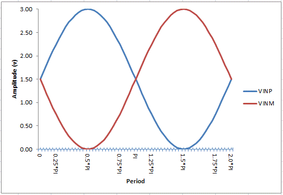
Now let me summarize my application as following:
A The input signals are AC voltages.
B I want to use 16-bit ADC,not 12-bit.
C My PCB is limited and there is not enough hardware transfer points to pass the analog signals.
D Suppose VREFHI=3V, VREFLO=0V,and the 1.5V bias has been done in the prefabricated analog circuit.

I read the "28377s manual" repeatedly, especially tables 9-3 and 9-5. After a lot of thinking, my final conclusion is that unless the full difference mode is used, the 16 bit ADC can only be used by 15 bits.At the same time, all the ADCIN_N signals are connected to the 1.5V.

I am not sure whether my analysis is correct or not, please correct it.
Thanks and best regards.

  • Hi K.K,

    You are correct.  The 16-bit mode ADC feature of the 28377S requires that the input signal to be differential mode and the following requirements need to be satisfied:

        - Need 2 ADC input pins to take the differential input.  The lower even channel is the positive input (VINP) and the higher numbered odd channel is the negative input  (VINM).  At any given time, the sum of the input voltages VINP and VINM should be equal to VREFHI value.  The common mode voltage is VREF/2, VREFCM.  Input signal variation should not exceed VREFCM +/-50mv.  Look under section 4.2 Signal Description of the 28377S datasheet  for ADC channel assignments of the specific 28377S device package you are using.

        - An example of a differential input pair is ADCINA2 and ADCINA3.  Say you chose VREF as 3V (VREFHI=3V and VREFLO=0v) and wanted to use the differential mode for 16-bit operation.  Input is an AC signal (3vpp - 3v max and 0v min, sine wave with a period of 2PI for illustration purposes, see figure below) you wanted to sample.  Feed ADCINA2 with the "positive" signal such that at time 0, VINP is 1.5v and ADCINA3 with the "negative" signal so at time 0, VINM is also 1.5v.  At time 0, VINP + VINM = 3V = VREFHI, which meets the criteria.  At time =.25*PI, VINP is at 2.25v and VINM is at 0.75v and so on.....  You should always meet the criteria that VINP+VINM is equal to VREFHI, with a tolerance of +/-50mv, to ensure that the ADC will operate within specifications.

    This is basically how a differential input pair works.  It is not just simply biasing the ADC channels to 1.5V and feeding the signal to an ADC input.  There are amplifiers that convert a single ended signal to differential output so you will not have to worry about producing the complementary signal on the VINM input.  Hope this clarifies your question.

    Best regards,

    Joseph

  • Hi K.K,

    Sorry, I forgot to include the attachment illustration for the input signals.

    Regards,

    Joseph

  • Thank you for your sincere and professional answer。
    You have interpreted and emphasized the ADC in the full differential mode.As a matter of fact, I have always been well aware of the ADC of the full difference mode.In essence with full difference mode, VINP=1.5+VIN/2, VINM=1.5-VIN/2. My bottleneck is that there are not enough hardware connection points.
    Now, we end this problem and continue to discuss the 3 issues that are related to it.
    1 Does TI have an integrated chip that converts a single ended signal to differential signals?It will meet VINP=1.5+VIN/2, VINM=1.5-VIN/2.
    2 According to the block diagram of DATASHEET in page 94, ADCIN14 and ADCIN15 are common input ports of 4 internal ADCs. Does that mean that these 2 ports can be configured to any one of ABCD? For example, configuring ADCINA14 and ADCINA15?Or ADCINC14 and ADCINC15?
    3 In the block diagram, ABCD's twelfth road input is also public, but with ADCINA0 together, what does it mean?

    Thank you again!
  • Hi K.K

    1) You can use a fully differential op-amp to turn a single-ended signal into a differential one with the correct common mode voltage.  For example, see the "Single-Ended Input to Differential Output Amplifier" circuit example in the THS4531 datasheet.  It is also possible to use 2 single-ended op-amps to do the conversion.  The best place to get help on this topic would be to create a new post in the Precision Amplifier forum.

    2+3) These pins that fan-out to multiple ADCs allow you some flexibility in choosing what ADC samples the pin.  For example, pin ADCIN14 could be sampled as input 14 on any ADC.  You could also sample the same reference voltage on multiple ADCs at the same time to try and eliminate ADC-to-ADC gain or offset error.   

  • Hi K.K,

    Please see my response below:

    1.) Yes, TI certainly has several products that cater to this application. Search in the ti.com website and look for fully differential amplifiers. There are several of these ICs, depending on spec requirement and application. For instance THS4551 is typically chosen for single supply rail application (from 2.7v to 5.4v) or THS413x for +5/-5V rails. VREFCM (common mode) is an input you can provide to the chip so it can be versatile depending on the reference voltage that is chosen.

    2.) Yes, ADCIN14 and 15 goes to all the ADC modules and you can use this as differential input pairs for all the ADCs (A,B,C or D).

    3.) ADCINA0 pin input also goes to all the ADC modules (channel 12) and this is also the output of DACA. It was configured this way such that user has the option to sample the output of the DAC on any of the ADCs - some applications may require a common reference signal for all the ADCs and to be compared later on (through comparator modules CMPSS or through SW by inspecting converted values on the ADCs) from various signal sources feeding through the different ADC modules.

    Let me know if this addresses your questions.

    Best regards,
    Joseph
  • Thank you for your answers above
  • Hi K.K,

    I'm closing this thread but if you have any unanswered questions regarding this topic, please feel free to post it in the forum.

    Regards,

    Joseph