This thread has been locked.

If you have a related question, please click the "Ask a related question" button in the top right corner. The newly created question will be automatically linked to this question.

TMS320F28377D: Using CLA and debugging for TMS320F28377D

Part Number: TMS320F28377D


Hi,

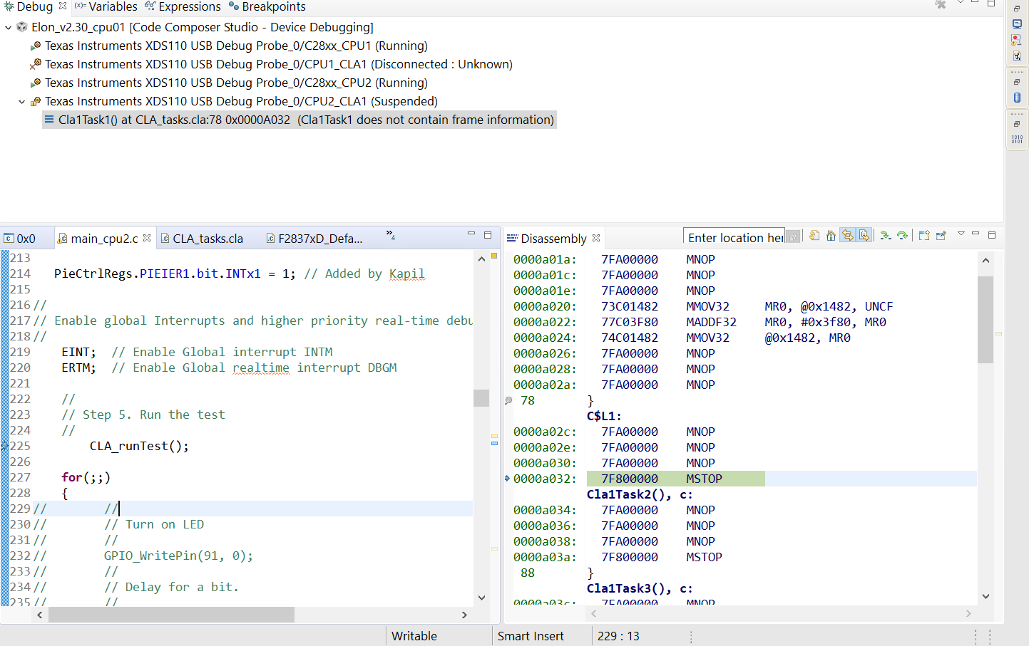
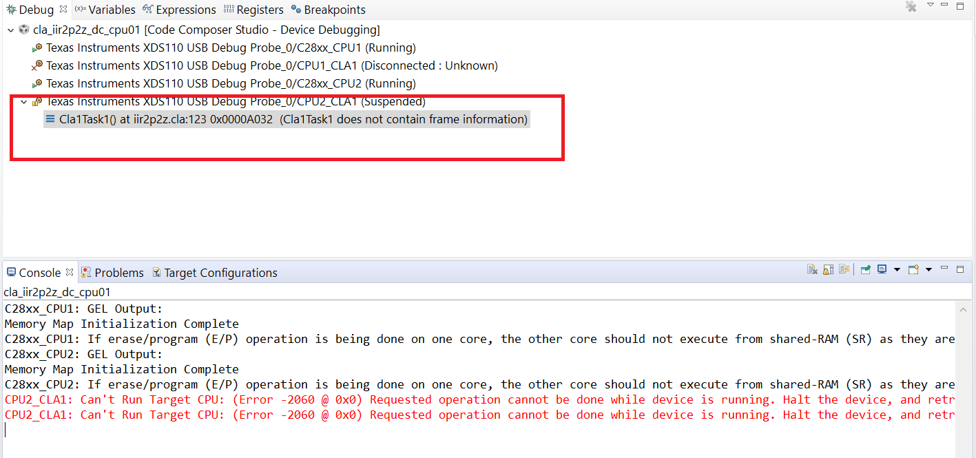
I am trying to use cla of cpu2. I took example code "cla_iir2p2z_dc_cpu01" & "cla_iir2p2z_dc_cpu01" as reference. When I try to debug this code, initially  "CLA_runTest();" function is executed and it is entering cla_task1 as it is expected. After its completion CLA is halted and when I  select CPU2_CLA1 and run, it is showing error as 

CPU2_CLA1: Can't Run Target CPU: (Error -2060 @ 0x0) Requested operation cannot be done while device is running. Halt the device, and retry the operation. (Emulation package 7.0.100.0)

Also, as shown in below attachment, it is showing that Cla1Task1 doesnot contain frame information.

What does this mean? How can I debug CLA?

Regards,

Lowkya

  • lowkya goli said:
    After its completion CLA is halted and when I  select CPU2_CLA1 and run, it is showing error as 

    If I understand, you are trying to start the CLA by pressing the "run" button in CCS.  If the CLA is idle it can only be started by a peripheral interrupt or by the C28x writing to the force register. 

    For guidance, the CLA hands-on-workshop is very good at describing the CLA, how to develop code for it, and also how to debug it in Code Composer Studio. I think you will find it helpful.

    Here is the link to the CLA workshop:

    Click here for more CLA FAQs and resources.

    I hope this helps. If this answers your question, please click the green "This resolved my issue" button.

    Regards,

    Lori

  • Hi Lori,

    Thanks for your response. I have gone through the workshop.

    I have tried using ADCINT1 interrupt as trigger aswell. From the start of main() I kept breakpoints at certain places while debugging and I was looking at disassembly. When code reaches "CLA_runTest()" ,  its halted at some point and when i look at disassembly it showing as below. In my code I have an ADC ISR along with CLA. Program is not going into that ISR also. Does this mean cpu2 is stuck somewhere?

    You can take a look at my initialization. 

    //
    // Included Files
    //
    #include "F28x_Project.h"
    #include "ElonCPU2_config.h"
    #include "math.h"
    #include "CLA.h"
    
    //
    // Defines
    //
    #define WAITSTEP     asm(" RPT #255 || NOP")
    
    //
    // Globals
    //
    //Task 1 (C) Variables
    // NOTE: Do not initialize the Message RAM variables globally, they will be
    // reset during the message ram initialization phase in the CLA memory
    // configuration routine
    
    #ifdef __cplusplus
    #pragma DATA_SECTION("CpuToCla1MsgRAM");
    float timer;
    #pragma DATA_SECTION("Cla1ToCpuMsgRAM");
    float result;
    #else
    #pragma DATA_SECTION(timer,"CpuToCla1MsgRAM");
    float timer;
    #pragma DATA_SECTION(result,"Cla1ToCpuMsgRAM");
    float result;
    #endif //__cplusplus
    
    #ifdef __cplusplus
    #pragma DATA_SECTION("CpuToCla1MsgRAM");
    float fVal;
    #pragma DATA_SECTION("Cla1ToCpuMsgRAM");
    float fResult;
    #else
    #pragma DATA_SECTION(fVal,"CpuToCla1MsgRAM");
    float fVal;
    #pragma DATA_SECTION(fResult,"Cla1ToCpuMsgRAM");
    float fResult;
    #endif //__cplusplus
    float y[BUFFER_SIZE];
    
    float asin_expected[BUFFER_SIZE]={
        1.570796, 1.393789, 1.320141, 1.263401, 1.215375,
        1.172892, 1.134327, 1.098718, 1.065436, 1.034046,
        1.004232, 0.9757544, 0.9484279, 0.9221048, 0.8966658,
        0.8720123, 0.8480621, 0.8247454, 0.8020028, 0.7797828,
        0.7580408, 0.7367374, 0.7158381, 0.6953120, 0.6751316,
        0.6552721, 0.6357113, 0.6164289, 0.5974064, 0.5786270,
        0.5600753, 0.5417370, 0.5235988, 0.5056486, 0.4878751,
        0.4702678, 0.4528166, 0.4355124, 0.4183464, 0.4013104,
        0.3843968, 0.3675981, 0.3509074, 0.3343180, 0.3178237,
        0.3014185, 0.2850964, 0.2688521, 0.2526802, 0.2365756,
        0.2205333, 0.2045484, 0.1886164, 0.1727327, 0.1568929,
        0.1410927, 0.1253278, 0.1095943, 0.09388787, 0.07820469,
        0.06254076, 0.04689218, 0.03125509, 0.01562564
    };
    
    uint16_t pass=0;
    uint16_t fail=0;
    
    //
    // Function Prototypes
    //
    void CLA_runTest(void);
    void CLA_configClaMemory(void);
    void CLA_initCpu2Cla1(void);
    
    __interrupt void cla1Isr1();
    __interrupt void cla1Isr2();
    __interrupt void cla1Isr3();
    __interrupt void cla1Isr4();
    __interrupt void cla1Isr5();
    __interrupt void cla1Isr6();
    __interrupt void cla1Isr7();
    __interrupt void cla1Isr8();
    
    #ifdef _FLASH
    //
    // These are defined by the linker (see device linker command file)
    //
    extern Uint16 RamfuncsLoadStart;
    extern Uint16 RamfuncsLoadSize;
    extern Uint16 RamfuncsRunStart;
    #endif
    
    static byte AnmuxSel = 1;
    struct Ang_Feedback *Filt_Fb =  &FilteredFb;
    
    void main(void)
    {
        //
        // Copy time critical code and Flash setup code to RAM
        // This includes InitFlash(), Flash API functions and any functions that are
        // assigned to ramfuncs section.
        // The  RamfuncsLoadStart, RamfuncsLoadEnd, and RamfuncsRunStart
        // symbols are created by the linker. Refer to the device .cmd file.
        //
        #ifdef _FLASH
          memcpy(&RamfuncsRunStart, &RamfuncsLoadStart, (size_t)&RamfuncsLoadSize);
        #endif
    
        //
        // Step 1. Initialize System Control:
        // PLL, WatchDog, enable Peripheral Clocks
        // This example function is found in the F2837xD_SysCtrl.c file.
        //
            InitSysCtrl();
    
        //
        // Call Flash Initialization to setup flash waitstates
        // This function must reside in RAM
        //
        #ifdef _FLASH
           InitFlash();
        #endif
    
    
    // Initialize all ADCS
        ConfigureADC_A();
        ConfigureADC_B();
        ConfigureADC_C();
        ConfigureADC_D();
        SetupADCA_Epwm();
        SetupADCB_Epwm();
        SetupADCC_Epwm();
        SetupADCD_Epwm();
    
     GpioDataRegs.GPADAT.all         = 0x77800000;
     GpioDataRegs.GPBDAT.all         = 0x02000000;
     GpioDataRegs.GPCDAT.all         = 0x0C000010;
    //
    // Step 3. Clear all interrupts and initialize PIE vector table:
    // Disable CPU interrupts
    //
        DINT;
    
    
        InitPieCtrl();
    
    //
    // Disable CPU interrupts and clear all CPU interrupt flags:
    //
        IER = 0x0000;
        IFR = 0x0000;
    
    
        InitPieVectTable();
    
        //
        // Step 3. Configure the CLA memory spaces first followed by
        // the CLA task vectors
        //
        CLA_configClaMemory();
        CLA_initCpu2Cla1();
    
    //
    // Initialize the Device Peripherals:EpwmS
    //
        EALLOW;
        CpuSysRegs.PCLKCR0.bit.TBCLKSYNC =0;
        EDIS;
    
        InitEPwm1Example();
        InitEPwm2Example();
        InitEPwm3Example();
        InitEPwm4Example();
        InitEPwm5Example();
        InitEPwm6Example();
        InitEPwm7Example();
        InitEPwm11Example();
    
        EPwm11Regs.ETSEL.bit.SOCAEN = 1;  //enable SOCA
    
        EALLOW;
        CpuSysRegs.PCLKCR0.bit.TBCLKSYNC =1;
    
        EDIS;
    
        ///////////////////////////////////////Added by Kapil
        EALLOW;
    
        PieVectTable.ADCA1_INT = &ADCA1_ISR;
        EPwm3Regs.TBCTL.bit.PHSEN = TB_DISABLE;
        EPwm4Regs.TBCTL.bit.PHSEN = TB_DISABLE;
    
        EDIS;
        /////////////////////////////////////////
    //
    // Enable CPU INT3 which is connected to EPWM1-3 INT:
    //
        IER |= M_INT3;
    //
    // Enable CPU INT1 which is connected to CPU-Timer 0:
    //
       IER |= M_INT1;
    
    //
    // Enable EPWM INTn in the PIE: Group 3 interrupt 8
    //
      //  PieCtrlRegs.PIEIER3.bit.INTx8 = 1;
    
    // Enable TINT0 in the PIE: Group 1 __interrupt 7
    
    //  PieCtrlRegs.PIEIER1.bit.INTx7 = 1;
    
       //Enable ADC1 interrupt in the PIE
    
       PieCtrlRegs.PIEIER1.bit.INTx1 = 1; // Added by Kapil
    
    //
    // Enable global Interrupts and higher priority real-time debug events:
    //
        EINT;  // Enable Global interrupt INTM
        ERTM;  // Enable Global realtime interrupt DBGM
    
        //
        // Step 5. Run the test
        //
            CLA_runTest();
    
        for(;;)
        {
    //        //
    //        // Turn on LED
    //        //
    //        GPIO_WritePin(91, 0);
    //        //
    //        // Delay for a bit.
    //        //
    //        DELAY_US(1000 * 250);
    //
    //        //
    //        // Turn off LED
    //        //
    //        GPIO_WritePin(91, 1);
    //        //
    //        // Delay for a bit.
    //        //
    //        DELAY_US(1000 * 250);
    
    //        PFC_ENABLE;
            SRCP_ENABLE;
            SRCHV_ENABLE;
            SRCLV_ENABLE;
    
            switch(AnmuxSel)
            {
            case MUX0:
                AnmuxSel =MUX1;
                break;
            case MUX1:
                FilteredFb.SRCP_SC = Filt_Fb->ANMux_Fb2;
    //            AnmuxSel =MUX2;
                break;
            case MUX2:
    //            FilteredFb.SRCHV_SC = Filt_Fb->ANMux_Fb2;
                AnmuxSel =MUX3;
                break;
            case MUX3:
                AnmuxSel =MUX4;
                break;
            case MUX4:
                AnmuxSel =MUX5;
                break;
            case MUX5:
                AnmuxSel =MUX6;
                break;
            case MUX6:
                AnmuxSel =MUX7;
                break;
            case MUX7:
                AnmuxSel =MUX0;
                break;
            }
            // Set Anmux data register
    //        SET_Anmux_Data(AnmuxSel);
            GpioDataRegs.GPCDAT.bit.GPIO80 = 1;
            GpioDataRegs.GPCDAT.bit.GPIO81 = 0;
            GpioDataRegs.GPCDAT.bit.GPIO82 = 0;
    
        }
    
            asm ("          NOP");
    }
    
    //
    // CLA_runTest - Run CLA test
    //
    void CLA_runTest(void)
    {
        int16_t i, error;
    
        for(i=0;i<BUFFER_SIZE;i++)
        {
            fVal= (float)(BUFFER_SIZE - i)/(float)BUFFER_SIZE;
            Cla1ForceTask1andWait();
            y[i] = fResult;
            error = fabs(asin_expected[i]-y[i]);
    
            if(error < 0.1)
            {
            pass++;
            }
            else
            {
            fail++;
            }
        }
    
    #if 0
    
        Cla1ForceTask2andWait();
        WAITSTEP;
    
        Cla1ForceTask3andWait();
        WAITSTEP;
    
        Cla1ForceTask4andWait();
        WAITSTEP;
    
        Cla1ForceTask5andWait();
        WAITSTEP;
    
        Cla1ForceTask6andWait();
        WAITSTEP;
    
        Cla1ForceTask7andWait();
        WAITSTEP;
    
        Cla1ForceTask8andWait();
        WAITSTEP;
    #endif
    }
    
    //
    // CLA_configClaMemory - Configure CLA memory
    //
    void CLA_configClaMemory(void)
    {
        extern uint32_t Cla1funcsRunStart, Cla1funcsLoadStart, Cla1funcsLoadSize;
    
        //
        // Wait for signal from CPU1 before configuring
        //
        IpcSync(5);
    
        EALLOW;
    #ifdef _FLASH
        //
        // Copy over code from FLASH to RAM
        //
        memcpy((uint32_t *)&Cla1funcsRunStart, (uint32_t *)&Cla1funcsLoadStart,
               (uint32_t)&Cla1funcsLoadSize);
    #endif //_FLASH
    
    #ifdef CPU2
        //
        // Enable CPU2 clocking at the sys clock level
        //
        CpuSysRegs.PCLKCR0.bit.CLA1 = 1;
    #endif //CPU2
    
        //
        // Initialize and wait for CLA1ToCPUMsgRAM
        //
        MemCfgRegs.MSGxINIT.bit.INIT_CLA1TOCPU = 1;
        while(MemCfgRegs.MSGxINITDONE.bit.INITDONE_CLA1TOCPU != 1){};
    
        //
        // Initialize and wait for CPUToCLA1MsgRAM
        //
        MemCfgRegs.MSGxINIT.bit.INIT_CPUTOCLA1 = 1;
        while(MemCfgRegs.MSGxINITDONE.bit.INITDONE_CPUTOCLA1 != 1){};
    
        //
        // Select LS4RAM and LS5RAM to be the programming space for the CLA
        // First configure the CLA to be the master for LS4 and LS5 and then
        // set the space to be a program block
        //
        MemCfgRegs.LSxMSEL.bit.MSEL_LS4 = 1;
        MemCfgRegs.LSxCLAPGM.bit.CLAPGM_LS4 = 1;
        MemCfgRegs.LSxMSEL.bit.MSEL_LS5 = 1;
        MemCfgRegs.LSxCLAPGM.bit.CLAPGM_LS5 = 1;
    
        //
        // Next configure LS0RAM and LS1RAM as data spaces for the CLA
        // First configure the CLA to be the master for LS0(1) and then
        // set the spaces to be code blocks
        //
        MemCfgRegs.LSxMSEL.bit.MSEL_LS0 = 1;
        MemCfgRegs.LSxCLAPGM.bit.CLAPGM_LS0 = 0;
    
        MemCfgRegs.LSxMSEL.bit.MSEL_LS1 = 1;
        MemCfgRegs.LSxCLAPGM.bit.CLAPGM_LS1 = 0;
    
        EDIS;
    }
    
    //
    // CLA_initCpu2Cla1 - Initialize CLA1 task vectors and end of task ISRs
    //
    void CLA_initCpu2Cla1(void)
    {
        //
        // Compute all CLA task vectors
        // On Type-1 CLAs the MVECT registers accept full 16-bit task addresses as
        // opposed to offsets used on older Type-0 CLAs
        //
        EALLOW;
        Cla1Regs.MVECT1 = (uint16_t)(&Cla1Task1);
        Cla1Regs.MVECT2 = (uint16_t)(&Cla1Task2);
        Cla1Regs.MVECT3 = (uint16_t)(&Cla1Task3);
        Cla1Regs.MVECT4 = (uint16_t)(&Cla1Task4);
        Cla1Regs.MVECT5 = (uint16_t)(&Cla1Task5);
        Cla1Regs.MVECT6 = (uint16_t)(&Cla1Task6);
        Cla1Regs.MVECT7 = (uint16_t)(&Cla1Task7);
        Cla1Regs.MVECT8 = (uint16_t)(&Cla1Task8);
    
        //
        // Enable the IACK instruction to start a task on CLA in software
        // for all  8 CLA tasks. Also, globally enable all 8 tasks (or a
        // subset of tasks) by writing to their respective bits in the
        // MIER register
        //
        Cla1Regs.MCTL.bit.IACKE = 1;
        Cla1Regs.MIER.all = 0x00FF;
        DmaClaSrcSelRegs.CLA1TASKSRCSEL1.bit.TASK1 = 6;//40//Task 1 (MVEC 7) is used to trigger on ADCINT1
    
        //
        // Configure the vectors for the end-of-task interrupt for all
        // 8 tasks
        //
        PieVectTable.CLA1_1_INT = &cla1Isr1;
        PieVectTable.CLA1_2_INT = &cla1Isr2;
        PieVectTable.CLA1_3_INT = &cla1Isr3;
        PieVectTable.CLA1_4_INT = &cla1Isr4;
        PieVectTable.CLA1_5_INT = &cla1Isr5;
        PieVectTable.CLA1_6_INT = &cla1Isr6;
        PieVectTable.CLA1_7_INT = &cla1Isr7;
        PieVectTable.CLA1_8_INT = &cla1Isr8;
    
        //
        // Enable CLA interrupts at the group and subgroup levels
        //
        PieCtrlRegs.PIEIER11.all = 0x00FF;
        IER |= (M_INT11 );
    }
    
    //
    // cla1Isr1 - CLA1 ISR 1
    //
    __interrupt void cla1Isr1 ()
    {
        //
        // Turn on LED
        //
        GPIO_WritePin(91, 0);
        //
        // Delay for a bit.
        //
        DELAY_US(1000 * 250);
    
        //
        // Turn off LED
        //
        GPIO_WritePin(91, 1);
        //
        // Delay for a bit.
        //
        DELAY_US(1000 * 250);
    
        //
        // Acknowledge the end-of-task interrupt for task 1
        //
        AdcbRegs.ADCINTFLGCLR.bit.ADCINT1 = 1; //clear INT1 flag
        PieCtrlRegs.PIEACK.all = M_INT11;
    //    asm(" ESTOP0");
    }
    
    //
    // cla1Isr2 - CLA1 ISR 2
    //
    __interrupt void cla1Isr2 ()
    {
        asm(" ESTOP0");
    }
    
    //
    // cla1Isr3 - CLA1 ISR 3
    //
    __interrupt void cla1Isr3 ()
    {
        asm(" ESTOP0");
    }
    
    //
    // cla1Isr4 - CLA1 ISR 4
    //
    __interrupt void cla1Isr4 ()
    {
        asm(" ESTOP0");
    }
    
    //
    // cla1Isr5 - CLA1 ISR 5
    //
    __interrupt void cla1Isr5 ()
    {
        asm(" ESTOP0");
    }
    
    //
    // cla1Isr6 - CLA1 ISR 6
    //
    __interrupt void cla1Isr6 ()
    {
        asm(" ESTOP0");
    }
    
    //
    // cla1Isr7 - CLA1 ISR 7
    //
    __interrupt void cla1Isr7 ()
    {
        asm(" ESTOP0");
    }
    
    //
    // cla1Isr8 - CLA1 ISR 8
    //
    __interrupt void cla1Isr8 ()
    {
        //
        // Acknowledge the end-of-task interrupt for task 8
        //
        PieCtrlRegs.PIEACK.all = M_INT11;
    //    asm(" ESTOP0");
    }
    
    //
    // End of file
    //
    

  • Hello,

    It often helps to debug one thing at a time to check the configuration of each part.  

    • If you don't enable the CLA, does the C28x take ADC interrupt as you expect?
    • If you setup the CLA and have the C28x SW force the ADC CLA task, does the task execute?
    • After the case above, when the task completes, does the C28x take the associated claISR from the PIE?
    • The CLA is edge triggered (not level triggered). The task has to be enabled when the interrupt comes in for the CLA to see the edge. This means that if a interrupt has already been flagged when the CLA task is enabled, then  it will be missed by the CLA.  This may mean re-ordering of your initialization and/or making sure no interrupts are flagged when the CLA task is enabled.

    Regards

    Lori

  • Hi Lori,

    I have debugged as you suggested. I observed that when I trigger CLA using interrupt, its working fine but when I trigger task using software(by setting IACK bit), CLA seems to be not executing the task. Do I just have to set IACK bit for software trigger or anything else to be done to trigger the task?

    Thanks,

    Lowkya

  • Lowkya,

    Please see this FAQ regarding SW triggering a task. 

    https://e2e.ti.com/support/microcontrollers/c2000/f/171/p/795549/2942520#2942520

    Regards

    Lori