


Part Number: TMS320F28069M
Hi,
We are doing the design for TMS320F28069U-PZPA with reference to Texas instruments F2806x ISO ControlCard design Documents.
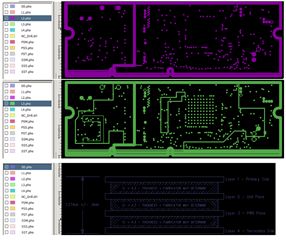
We have one doubts on the Gerber data. PFA the image from Gerber Data and also Gerber files, In the Gerber data, Layer 2 and Layer3 are only Wider Tracks not the complete copper Plane right?
 FAB_{TEX116}F2806xISOcontrolCARDr0.4.zip
Can we do dedicated complete copper plane for Layer2(Ground) and Layer3(Power)?
Thanks and regards,
Naveen K
