


Hello,
I'm using a TMS570LS3137 and SafeRTOS to receive and transmit datagrams via SCI and RS485 with aid of DMA. Therefore, I wait for the DMA block transfer complete interrupts to toggle the transmit enable line of the transceiver. So, there's a bidirectional communication via half-duplex RS485. This works fine for reception. But with transmission I get the DMA BTC interrupt two bytes too early.
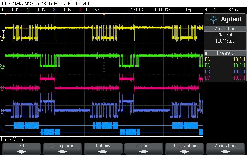
Please find attached an oscilloscope screenshot: Yellow is Rx, green is Tx, red is the transceiver transmit enable line, and blue is the resulting RS485 bus signal. Since the DMA transmit BTC interrupt is triggered too early, transmitted datagrams are cut off. I could verify that the transceiver transmit enable signal (red) goes to low at the moment when the DMA transmit BTC interrupt is triggered. I've also attached the DMA init function, the SCI init function and a schematic representation of the DMA interrupt service routine. Please ignore the burst on Rx and Tx when the transceiver transmit enable line goes to low.
Do you have any idea what is going wrong?
Thank you in advance!
Andre
void dmaInit(){

   /* TX line, DMA configuration for transmission via SCI bus */
   dmaReqAssign((uint32)DMA_CH0, 31U); /* assign request line 31 (SCI transmit) to channel 0 */
   dmaEnableInterrupt((uint32)DMA_CH0, (dmaInterrupt_t)BTC); /* enable interrupt for block transfer complete */
   /* setting DMA control packets for transmit */
   g_dmaCTRL dma_control_TX;
   dma_control_TX.SADD = (uint32) &g_datagramToSend; /* initial source address */
   dma_control_TX.DADD = ((uint32)&(sciREG->TD)) + 3U; /* initial destination address (big endian!) */
   dma_control_TX.CHCTRL = 0U; /* is overwritten by some of the next commands */
   dma_control_TX.FRCNT = 7U; /* frame count (ITCOUNT) */
   dma_control_TX.ELCNT = 1U; /* element count (ITCOUNT) */
   dma_control_TX.ELDOFFSET = 0U; /* element destination offset */
   dma_control_TX.ELSOFFSET = 0U; /* element source offset */
   dma_control_TX.FRDOFFSET = 0U; /* frame destination offset */
   dma_control_TX.FRSOFFSET = 0U; /* frame source offset */
   dma_control_TX.PORTASGN = 4U; /* channel 0 assigned to port B (PAR0) */
   dma_control_TX.RDSIZE = ACCESS_8_BIT; /* read element size */
   dma_control_TX.WRSIZE = ACCESS_8_BIT; /* write element size */
   dma_control_TX.TTYPE = FRAME_TRANSFER; /* trigger type - frame/block */
   dma_control_TX.ADDMODERD = ADDR_INC1; /* addressing mode for source */
   dma_control_TX.ADDMODEWR = ADDR_FIXED; /* addressing mode for destination */
   dma_control_TX.AUTOINIT = AUTOINIT_OFF; /* auto-init mode */
   dmaSetCtrlPacket((uint32)DMA_CH0, dma_control_TX);

   /* RX line, DMA request for reception via SCI bus */
   dmaReqAssign((uint32)DMA_CH1, 30U); /* assign request line 30 (SCI receive) to channel 1 */
   dmaEnableInterrupt((uint32)DMA_CH1, (dmaInterrupt_t)BTC); /* enable interrupt for block transfer complete */
   /* setting dma control packets for transmit */
   g_dmaCTRL dma_control_RX;
   dma_control_RX.SADD = ((uint32)&(sciREG->RD)) + 3U; /* initial source address */
   dma_control_RX.DADD = (uint32) &g_bufferedDatagram; /* initial destination address */
   dma_control_RX.CHCTRL = 0U; /* next ctrl packet to be trigger + 1 (CHCTRL) */
   dma_control_RX.FRCNT = 9U; /* frame count */
   dma_control_RX.ELCNT = 1U; /* element count */
   dma_control_RX.ELDOFFSET = 0U; /* element destination offset */
   dma_control_RX.ELSOFFSET = 0U; /* element source offset */
   dma_control_RX.FRDOFFSET = 0U; /* frame destination offset */
   dma_control_RX.FRSOFFSET = 0U; /* frame source offset */
   dma_control_RX.PORTASGN = 4U; /* channel 1 assigned to port B (PAR0) */
   dma_control_RX.RDSIZE = ACCESS_8_BIT; /* read element size */
   dma_control_RX.WRSIZE = ACCESS_8_BIT; /* write element size */
   dma_control_RX.TTYPE = FRAME_TRANSFER; /* trigger type - frame/block */
   dma_control_RX.ADDMODERD = ADDR_FIXED; /* addressing mode for source */
   dma_control_RX.ADDMODEWR = ADDR_INC1; /* addressing mode for destination */
   dma_control_RX.AUTOINIT = AUTOINIT_OFF; /* auto-init mode */
   dmaSetCtrlPacket((uint32)DMA_CH1, dma_control_RX);

   /* enable channel 1 for hardware triggering */
   dmaSetChEnable((uint32)DMA_CH1, (uint32)DMA_HW);
   /* enable DMA */
   dmaEnable();
}
void sciInit(void)
{
/* USER CODE BEGIN (2) */
/* USER CODE END */

    /** @b initialize @b SCI */

    /** - bring SCI out of reset */
    sciREG->GCR0 = 0U;
    sciREG->GCR0 = 1U;

    /** - Disable all interrupts */
    sciREG->CLEARINT    = 0xFFFFFFFFU;
    sciREG->CLEARINTLVL = 0xFFFFFFFFU;

    /** - global control 1 */
    sciREG->GCR1 =  (uint32)((uint32)1U << 25U)  /* enable transmit */
                  | (uint32)((uint32)1U << 24U)  /* enable receive */
                  | (uint32)((uint32)1U << 5U)   /* internal clock (device has no clock pin) */
                  | (uint32)((uint32)(1U-1U) << 4U)  /* number of stop bits */
                  | (uint32)((uint32)0U << 3U)  /* even parity, otherwise odd */
                  | (uint32)((uint32)0U << 2U)  /* enable parity */
                  | (uint32)((uint32)1U << 1U);  /* asynchronous timing mode */

    /** - set baudrate */
    sciREG->BRS = 3U;  /* baudrate */

    /** - transmission length */
    sciREG->FORMAT = 8U - 1U;  /* length */

    /** - set SCI pins functional mode */
    sciREG->PIO0 = (uint32)((uint32)1U << 2U)  /* tx pin */
                 | (uint32)((uint32)1U << 1U); /* rx pin */

    /** - set SCI pins default output value */
    sciREG->PIO3 = (uint32)((uint32)0U << 2U)  /* tx pin */
                 | (uint32)((uint32)0U << 1U); /* rx pin */

    /** - set SCI pins output direction */
    sciREG->PIO1 = (uint32)((uint32)0U << 2U)  /* tx pin */
                 | (uint32)((uint32)0U << 1U); /* rx pin */

    /** - set SCI pins open drain enable */
    sciREG->PIO6 = (uint32)((uint32)0U << 2U)  /* tx pin */
                 | (uint32)((uint32)0U << 1U); /* rx pin */

    /** - set SCI pins pullup/pulldown enable */
    sciREG->PIO7 = (uint32)((uint32)0U << 2U)  /* tx pin */
                 | (uint32)((uint32)0U << 1U); /* rx pin */

    /** - set SCI pins pullup/pulldown select */
    sciREG->PIO8 = (uint32)((uint32)1U << 2U)  /* tx pin */
                 | (uint32)((uint32)1U << 1U);  /* rx pin */

    /** - set interrupt level */
    sciREG->SETINTLVL = (uint32)((uint32)0U << 26U)  /* Framing error */
                      | (uint32)((uint32)0U << 25U)  /* Overrun error */
                      | (uint32)((uint32)0U << 24U)  /* Parity error */
                      | (uint32)((uint32)0U << 9U)  /* Receive */
                      | (uint32)((uint32)0U << 8U)  /* Transmit */
                      | (uint32)((uint32)0U << 1U)  /* Wakeup */
                      | (uint32)((uint32)0U << 0U);  /* Break detect */

    /** - set interrupt enable */
    sciREG->SETINT = (uint32)((uint32)0U << 26U)  /* Framing error */
                   | (uint32)((uint32)0U << 25U)  /* Overrun error */
                   | (uint32)((uint32)0U << 24U)  /* Parity error */
                   | (uint32)((uint32)0U << 9U)  /* Receive */
                   | (uint32)((uint32)0U << 1U)  /* Wakeup */
                   | (uint32)((uint32)0U << 0U);  /* Break detect */

    /** - initialize global transfer variables */
    g_sciTransfer_t[0U].mode   = (uint32)0U << 8U;
    g_sciTransfer_t[0U].tx_length = 0U;
	g_sciTransfer_t[0U].rx_length = 0U;

    /** - Finaly start SCI */
    sciREG->GCR1 |= 0x80U;
}
void dmaGroupANotification(dmaInterrupt_t inttype, uint32 channel)
{
   /* transmit BTC interrupt */
   if((channel == (uint32)DMA_CH0) && (inttype == (dmaInterrupt_t)BTC))
   {
      ...
      /* receive new datagram */
      triggerDmaReception();
   }

   /* datagram reception completed */
   if((channel == (uint32)DMA_CH1) && (inttype == (dmaInterrupt_t)BTC))
   {
      /* send datagram if datagram is pending */
      if(g_isDatagramWaitingToGetSent == 1U)
      {
         /* transmit pending datagram */
         triggerDmaTransmission();
      }
      else
      {
         /* receive new datagram */
         triggerDmaReception();
      }
   }
}

void triggerDmaReception()
{
   gioSetCanBit(canREG3, 0U, 0U); /* switch transceiver to reception */
   ...
   dmaSetChEnable((uint32)DMA_CH1, (uint32)DMA_HW); /* trigger DMA reception */
}

void triggerDmaTransmission()
{
   gioSetCanBit(canREG3, 0U, 1U); /* switch transceiver to transmission */
   ...
   dmaSetChEnable((uint32)DMA_CH0, (uint32)DMA_HW); /* trigger DMA transmission */
}

