This thread has been locked.

If you have a related question, please click the "Ask a related question" button in the top right corner. The newly created question will be automatically linked to this question.

SPI protocol between MSP430F449 and KXPS5

Other Parts Discussed in Thread: MSP430F449

Hello everyone! I am new with micro-controller and I have problems when establishing SPI interface between MSPF449 and KXPS5 accelerometer ( Kionix Inc.).

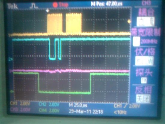
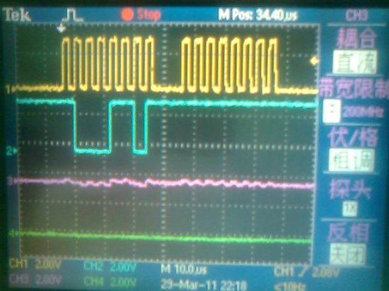
Here is the problem .I want to read back the content of KXPS5’s register. However, I could not get any useful data back. There is always 0x00 data on the MISO line. I think the initializing of the master is correct, because the data on SCK line and MOSI line appear correct (using oscillator). Maybe the initializing of the accelerometer is not correct, but I could not figure out.

The following are the connection and the code.

//*********************************************************

//          MSP430x44x       kionix  KX_S5

//         -------------|

//       |        P4.4  |---> nCS                     

//       |   UCLK/P3.3  |--->SCLK

//       |   SOMI/P3.2  |<---SDO

//       |   SIMO/P3.1  |--->SDI

//       |        P4.6  |--->Enable

//              

//**********************************************************

#include <MSP430x44x.h>

unsigned char control[4]={0x8D,0xFF,0x8C,0xFF};

//   read command:0x8D and 0x8C are the address of two register in KXPS5 ;

//    0xFF is dummy data send to KXPS5

unsigned char receive[4]={0xFF,0xFF,0xFF,0xFF}; // saving the data read back from KXPS5

unsigned char j=0;

void SPI_transfer(unsigned char txbyte)

{

  IFG1 |= URXIFG0;

  IE1 |= URXIE0;

}

void wait (int counts)

{

  __no_operation();

  do (counts--);

  while (counts != 0);

}

int main(void)

{

  WDTCTL = WDTPW + WDTHOLD;  

    SCFI0 |= FN_4;      //ACLK = LFXT1 =32768Hz

                      //MCLK = SMCLK =DCOCLK = (N+1)*2*ACLK 

  SCFQCTL = 121;      //(121+1)*32768*2=7.99MHz

  FLL_CTL0 = DCOPLUS + OSCCAP1;

  P3SEL = 0x0E;                   // Setup P3 for SPI mode                    

  P3DIR |= 0x0A;                       


  U0CTL = CHAR + SYNC + MM + SWRST;         // 8-bit, SPI, Master

  U0TCTL = CKPL + SSEL1 + STC;             // Polarity, 3-wire ,

// all the 4 clock mode I have tried, but nothing changed on the SOMI line.

  U0BR0 = 0x010;                            // SPICLK = SMCLK/2 = 4MHz

  U0BR1 = 0x000;

  U0MCTL = 0x000;

  ME1 = USPIE0;                             // Module enable

  U0CTL &= ~SWRST;                          // SPI enable


  P4DIR |= BIT6 + BIT4;

  P4OUT |= BIT4;

  P4OUT &= ~BIT6;                          // slave ENABLE

  P4OUT |= BIT6;

  wait (5000);

  _EINT();                                   // Enable interrupts


  while(1)

  {

    P4OUT |= BIT4;                  

    for (j=0;j<4;j++)

    {

      P4OUT |= BIT4;

      SPI_transfer (control[j]);

    }

    LPM0;                               // CPU off   

  }   

}

#pragma vector=USART0RX_VECTOR

__interrupt void SPI0_rx (void)

{

  P4OUT &= ~BIT4;                        // chip select //slave SPI enable

  TXBUF0 = control[j]; 

  while ((IFG1 & URXIFG0) == 1);         //  RX/TX ready?

  receive[j]=RXBUF0;

  j = j + 1;

  TXBUF0 = control[j]; 

  while ((IFG1 & URXIFG0) == 1);         // RX/TX ready?

  wait (200);

  receive[j]=RXBUF0;

  P4OUT |= BIT4;

  IE1 &= ~URXIE0;

} 

Here is the datasheet for KXPS5. 

http://www.kionix.com/Product-Specs/KXSS5-2057%20Specifications%20Rev%203.pdf

Please help me on this. Thank you very much!

PS: I am using both evaluation board of MSP430F449 and KXPS5.


  • Christine,

    Welcome to the E2E forum!

    Here are my comments:

    As per the diagram, the pin P4.5 is connected to the chip select of the slave. But the code has instruction for port P4.4 (e.g. P4OUT |= BIT4) instead of BIT5. Can this be the reason for the issue?

    Regards,

    Nag

    (If your question is answered, please click the Verify Answer button on this post)


  • Thank you, Nag!

    I must apologize for the mistake I made in the original post. I changed pins for nCS while trying to find whether it is wrong with the connection. Thus I forget to change the connection picture.

    Thank you for your efforts all the same!

    I can observe the voltage on the nCS from high to low during SPI communication, and finally goes high after SPI.

    So I  think I can control the nCS properly.

    Maybe there is wrong somewhere else. Hope for your reply! Thanks again!


  • Did you notice that SPI is bi-direcitonal synchronous?

    When you send the four command bytes, the slave hasn't yet received your command and therefore cnanot respond. To get the answer, you'll have to send additional dummy bytes over SPI in order to receive the answer.

    Also, there are some other oddities in your code:

    Christine said:
    P4OUT &= ~BIT6;                          // slave ENABLE
    P4OUT |= BIT6;

    this en-. and then immediately disables the slave. Usually (I didn't read the device datasheet), you assert CS and then do the transfer and then de-assert CS. Or is this intended to be sort of a slave reset?

    Christine said:
    wait (200);

    Why do you wait here? You already checked for a received byte (URXIFG0), so just read it.

    Christine said:
    P3SEL = 0x0E;                   // Setup P3 for SPI mode                   
     
    P3DIR |= 0x0a;

    No need to set P3DIR. The direction is controlled by the USCI module. (in case of I2C, the direction will even change during a transfer) On P3SEL, you shoudl use |= instead of = to avoid conflicts with other code that might already have changed the P3SEL register onteh other bits.


  • Thank you for your advice!

    1)  I do not quite understand the first advice you gave me. Each time I sent two command bytes (eg.0x8C, a control register address ), and then I sent additional dummy bytes 0xFF over SPI to receive the answer. Am I wrong with somewhere?

    2)  Following  is said in the datasheet.

        ENABLE pin                   high----------Normal operation

                                                transition from low to high---------------default values loaded into registers from eeprom

                                                low-----------device is in standby

        and nCS is used for SPI enable  (1= I2C mode ,  0= SPI mode)


  • Christine said:
    I do not quite understand the first advice you gave me. Each time I sent two command bytes (eg.0x8C, a control register address ), and then I sent additional dummy bytes 0xFF over SPI to receive the answer. Am I wrong with somewhere?

    No. I didn't know the command sequence and was seeing that you're sending a 4-byte sequence (of any meaning) and expect the result being sent before all 4 bytes have arrived at the slave. It's a common mistake with SPI. Also, teh double-buffering (and the required nesting logic with sendign and receiving) seems to be difficult to understand (or at least to notice) for many people. Yet if the command sequence is indeed just one byte and the following is the dummy to get the responst, then this part is fine.

    However...

    Christine said:
    Each time I sent two command bytes (eg.0x8C, a control register address ), and then I sent additional dummy bytes 0xFF
    Well, you send one command byte, then a 0xff byte, then another command byte and another 0xff byte. If that's what you meant, then it's fine.


    Christine said:
    ENABLE pin                   high----------Normal operation
                                                transition from low to high---------------default values loaded into registers from eeprom
                                                low-----------device is in standby

    So this is jsut a 'device on/off' signal.

    Christine said:
    and nCS is used for SPI enable  (1= I2C mode ,  0= SPI mode)

    and this one selecs the transfer mode. But looking into the datasheet, it seems that this signal also starts an SPI transfer.
    I wonder whether the device will accitentally respond to an SPI command sent to another slave if it matches its own I2C address (nCS is high = I2C mode = device is listening for its I2C address). I think to avoid this, you must ensure that your initialization and handling of the SPI bus does not lead to an accidental I2C start condition. (high-to-low transition on the SDA/SIMO line while SCL is high)

    So what's wrong...

    I sit possible that you're just too fast? You set SPICLK to SMCLK/2 and SMCLK is 8MHz. But the device has a mnaximum SPI clock of 1MHz. Or, to be exact, some pulse lengths have to be at least 350ns, which (since the MSP uses uniform timing) is 1.428MHz at max. Even the best case of 130ns pulse width (between single bits) would equal to no more than 3.846MHz. So I guess the device is just not 'hearing' your signals.

    Another thing:

    your 'wait' function is probably not working as expected. It is a 'pure' function. That means it completely works on its parameters and ha sno side effects. But it also does not have a return parameter. Depending on compiler smartness, the loop inside might be optimized away (since at the end of the loop, all that ahs happened is that 'counts' is 0).
    Worst case is that the compiler will remove the funciton call completely as it is irrelevant.
    Using __delay_caycles() would do a delay, but it only works for a constant number of cycles. You could include a __NOP() in the counting loop, or a __delay_cycles(1). But still the outcome is not 100% predictable, as it depends on the current MCLK speed.
    Best was for a delay is to use a timer. Either set up a timer for a certain speed, start it and wait until a given numeber of ticks has passed, or you program a CCR unit to set its IFG bit when the timer has performed a given number of ticks. Or for larger delays, program an interrupt function that counts milliseconds in a global counter and wait until it has reached/was increased by a certain value. In most projects, you'll need this kind of functionality anyway when you get past the initial playing.

  • 1)  There is only one master and one slave. And in the main function, the initialization of the master is set to SPI. So I wonder whether this can avoid an accidental  IIC condition.


    2)  I set SPICKL to 125kHz and SMCLK is 4MHz .  I add wait functions in the interrupt function and use oscilator to check whether delay is working. Here is the picture I got.

    line 1 :SCLK

    line 2:MOSI

    line 3:MISO

    line 4 : nCS

    I sent command byte 0x8D first and sent dummy byte oxFF on line MOSI.

    Wait function is added right after nCS set low, between the two bytes and after the second byte sent. I wonder whether the wait function works.


     For specific:

    There is only noise on the line MISO. It seems that the slave does not respond at all.


  • Shouldn't the clock be idle-high and active low? It's opposite on your screenshots. It looks like eithe rpolarityor phase are wrong. Looking into the datasheet again, the bit is taken on the rising edge of the signal and has to be stable for some time before and after the rising edge. On teh screenshot, however, it seems that the MOSI signal is changing at the rising edge of the clock signal. Which indicates a wrong polarity or phase setting.

    The noisy line of the SOMI signal, however, almost looks like the slave output is not enabled at all, as if the device were nor there. If the SPI is active, no matter whether soemthign is actually read, it should pull the SOMI line high or low, but not be in tri-state (except in I2C mode, when the internal pullups are disabled). But if it were active, there shouldn't be so much visible crosstalk on the SOMI line.
    Theoretically, when nCS goes low, the pullsp shoudl be activated and SOMI should go high (unless something else is transmitted)

    Are you sure you're applying nCS properly? Is the sensor powered and enabled? Bad soldering?

  • My problem has been solved. It is due to bad connection.

    Thank you for your advices!

**Attention** This is a public forum