This thread has been locked.

If you have a related question, please click the "Ask a related question" button in the top right corner. The newly created question will be automatically linked to this question.

MSPM0G3507-Q1: The rise and fall rate on the MSPM0G3507 general input.

Part Number: MSPM0G3507-Q1
Other Parts Discussed in Thread: TXB0104, MSPM0G3507

Does it matter when the input signal rises or falls between 0-3.3V at a super low rate(several minutes)? The GPIO of M0G3507 was configured as an edge-triggered input. The reason I ask is that we once had some problems using the level shifter product (TXB0104), which has a maximum rise and fall rate limit.

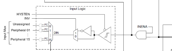
  • The hysteresis of the Schmitt trigger should help you there. You can also turn it on or off.

    Though I am not sure how that AND gate will affect things, it seems to defeat the purpose of the schmitt trigger.

  • It do provide the hysteresis function for IO.

  • What do you mean by "it"? According to the diagram the hysteresis providing schmitt trigger is inside the "input logic box" isolated by the AND gate.

    I assume that the AND gate is actually an analog transmission gate, or the schmitt trigger is useless.

  • "It" means HYSTEN bit in TRM or HYSTEN in your diagram.

    After enable this, if run some voltage test, the hysteresis behavior will be seen on the waveform.

  • Right, so the AND gate in front of the Schmitt trigger that is controlled by that bit must be a transmission gate, not a digital AND gate or the hysteresis would not take affect on any input signal, since it would be buffered by a digital AND gate.

  • Which gate are you referring to? The INENA?

    Your concern is correct, but I think this should be a diagram issue here.

    INENA must enable for a input IO, while during the hysteresis test, we can still see the hysteresis behavior.

    Very good aspect, I will check this part with docs team to make sure everything in a correct position.

  • Yes, thank you that is exactly to what I am referring to here. As I said, I suspect it is actually an analog transmission gate.

  • Does this mean that the Schmitt trigger is indeed at the very beginning of the input path?

    Since it has the schmitt trigger here, the false trigger is unlike to happen. However, since our input edge is extremely slow (several minutes per volt), will problems such as high current and overheating occur? Since the transistors inside the io structure may partially on for a long time.

  • Does this mean that the Schmitt trigger is indeed at the very beginning of the input path?

    This is only the function diagram to better show you each function and register bit's relationship, actual circuit not looks like this.

    So don't worry about this.

    Since it has the schmitt trigger here, the false trigger is unlike to happen. However, since our input edge is extremely slow (several minutes per volt), will problems such as high current and overheating occur? Since the transistors inside the io structure may partially on for a long time.

    First, 

    It is necessary to ensure that the input voltage and current do not exceed 7.1 Absolute Maximum Ratings in the datasheet and remain within 7.3 Recommended Operating Conditions is enough.

    Second,

    There will be a little bit large current in such working scenario for schmitt, we can not avoid this.

    Since this current is not indicated in datasheet, you need to run actual test to confirm the current.

    And if only one or two IO used in this mode, if you can accept the large current, it should be ok as long as there is sufficient heat dissipation.

    Does it matter when the input signal rises or falls between 0-3.3V at a super low rate(several minutes)?

    GPIO is not a best choice for this use case here.

    COMP:

    In MSPM0G3507, you can choose to use a COMP with Hysteresis 30mV enabled, to convert this kind of low slew rate signal to logic signal.

    ADC:

    You can also try to use a ADC with Window Comparator enabled, you can set any low/high threshold code of ADC result as interrupt.

  • Is COMP or ADC still available in standby mode? Currently we use this fall edge as the wakeup source to change the mcu from STANDBY to RUN mode.

  • COMP works in STB0 mode.

    ADC need STOP mode.

    Please refer to datasheet Table 8-1. Supported Functionality by Operating Mode for more information.

  • "However, since our input edge is extremely slow (several minutes per volt), will problems such as high current and overheating occur? Since the transistors inside the io structure may partially on for a long time."

    The input impedance of the input is very high and draws very little current. It can sit for *years* at any given voltage with no issue.

  • According to SCEA046B, the peak current is approximately 2mA (Not sure if this value can be applied to the MSPM0G series). Since I only have one pin function in this way, it shouldn't be a problem, right?

  • The input impedance of the input is very high and draws very little current. It can sit for *years* at any given voltage with no issue.

    I think there is some schmitt trigger issue in thie scenario, I'm not a analog expert, but after doing some research, I found it's possible to cause high current in very low slew rate voltage input.

    (Not sure if this value can be applied to the MSPM0G series)

    From MSPM0 hardware itself, IO has ability to output/input 2mA current.

    But not sure whether it's acceptable in this kind of usage.

    7.1 Absolute Maximum Ratings -> IIO Current of SDIO pin 6 mA -> I guess it's OK.

    But still not recommend to use in this way, we got COMP solution which is better.

**Attention** This is a public forum