This thread has been locked.

If you have a related question, please click the "Ask a related question" button in the top right corner. The newly created question will be automatically linked to this question.

USB schematic question regarding MSP430F6x chips

Could someone give me some feedback on what exactly you need to connect up an MSP430 to USB and successfully get USB communication?  I'm somewhat new to USB.  I noticed there are a few passives in a schematic I got from SLA514 app note.  I've just connected up DP, DM and VBUS.  It sounds to me like you can either use hardware pullups or software pullups for Full speed mode.  So does this mean if I don't pull up VUSB in hardware (leave it disconnected) I can pull it up in software?  Also is VBUS the only USB power I need to connect up?  For DP and DM do I need series resistors and capacitors like shown in the USB portion of the app note linked below or will a one to one connection between connector and pins be fine?  Just looking for some clarification here so I can spin a basic board and start working on simple USB stuff.

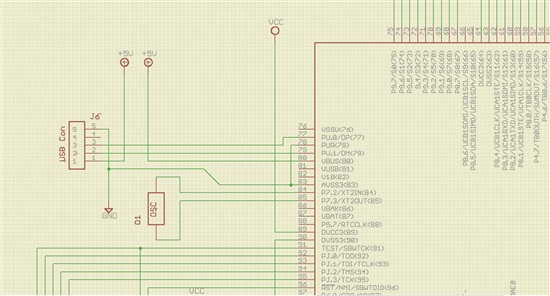
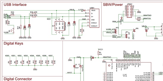
I've attached a screen shot of my schematics showing the USB portion as well as a screenshot of TI's USB circuit from the app note

http://www.ti.com/lit/an/slaa514/slaa514.pdf

Thanks,

Rob

My schematic

TI's from app note

  • Robbie Valentine said:
    successfully get USB communication?

    1. Make sure that your D+/- traces are routed as 90-ohm differential pairs (controlled impedance)

    2. If this circuit is ever going to be used outside of just sitting on your lab bench, then you need to add ESD protection to the lines, as close to the connector as possible.

  • DP/DM pins from chip can be connected over 27R resistor to USB connector. PUR pin is used for USB BSL. Diode on VBUS (USB connector) is for USB port protection. 1.5 K resistor between +3.3V and DP can be used for full speed device detection. Follow app note, but if USB dev board will be used just in office from you, don't worry too much about design. My first MSP430F550x USB dev board DIY P2P, was used for developing my own USB stack. Didn't have any problems, with highest transfer rate 1 MB/s. Now have 2, DIY P2P board, and there are still my main boards for development, and I am working on USB related staff.

  • So what are the R35_27R resistors for?  Are these the 90 ohm impedances you mentioned or are these 27 ohms?  Also, soli thanks for the response.  For  a usb BSL (boot strap loader), do you just tie PUR to DP?

    Also, What is the difference between VBUS and VUSB?  It looks like from the datasheet for these chips (family datasheets) that VBUS can provide all the power you need for the MSP's USB module. 

  • VBUS is 5V supply for USB module. VUSB is 3.3V internal regulator output, that can be used for rest of the MSP430 system (AVCC/DVCC). For BSL, button is used that is connecting +3.3V (AVCC/DVCC) over 100R resistor to PUR pin, so when button is pressed and chip is powered (USB cable connected to PC), PUR will be HI (+3.3V) and it will enter to BSL mode. PUR is connected over 1k4 resistor to DP.

  • Ok that makes sense.  So, just to make sure I'm on the right track here, in that picture where PUR and DP are pulled down by a 1M ohm resistor means that you aren't using full speed mode?  I thought for full speed mode you had to pull DP up to 3.3.  It looks like DP is tied to ground through the 1M just like PUR is.  Is that correct or am I missing something?  Also, if you don't externally pull up DP it sounds  like (from the family datasheet) that you can pull it up in software.  Is that correct?

    Thanks,

    Rob

  • 1M resistor is probably there to not have floating PUR pin, and it is not available on some boards (NA marking on some schematics). It is not directly related to DP. 1k4 resistor between PUR and DP is for full speed mode detection, and it is activated by software during USB setup process (bis.w #PUR_EN, &USBCNF).

  • I wanted to get a second opinion on two things real quick.  1. Is my routing ok in the attached picture?  I'm just not sure if routing the DP/DM lines under my 4Mhz oscillator is a good idea or not noise wise.  Does anyone have any input on how i'm thinking about routing this?  2.  Why are the DP and DM lines opposite of the standard connector.  I have to split them on top and bottom layers and then cross them to get to the correct MCU pins.  I've checked this a lot and from everything I can find in datasheets and online My parts are correct.  Am I missing something?  I would think that they would just run parallel to the MCU pins and not have to cross...just seems wrong to me.  Any input on either would be greatly appreciated!

    Thanks,

    Rob

  • 1. If the USB/XT pins are not mixed on chip body, there is no need to go with USB lines under XT. It will work, but don't see any reason for do it on this way.

    2. DP/DM on two layers will work (and all TI board done on this way), but there is possibility to have both lines on one top layer.

    http://forum.43oh.com/topic/1196-f5529-breakout-dev-board-now-with-pics/?p=10172

**Attention** This is a public forum