This thread has been locked.

If you have a related question, please click the "Ask a related question" button in the top right corner. The newly created question will be automatically linked to this question.

MSP430G2553 Problem to feed external clock from XIN to MCLK

Other Parts Discussed in Thread: MSP430G2553

Hello MSP430-Experts !

I'm very happy with my LaunchPad for some time now.

At the moment I try to switch MCLK from DCO-Clock of 8 MHz   to  an external XTAL-Oscillator clock of 2 MHz.

As a cross check I'm using a toggling pin and a scope - - -   five clocks per toggle instruction can be observed.

However, I don't see any change in behavior of the toggling - it stays at  5 x 125 ns  !

My code is:

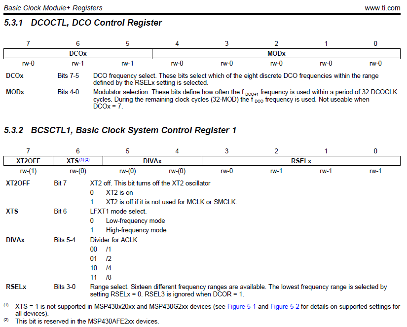
BCSCTL1 = CALBC1_8MHZ;   // Set DCO to 8 MHz

DCOCTL = CALDCO_8MHZ;

// P2.6 is normally INPUT by default ! now used as XIN only ...

_BIC_SR( OSCOFF );  // reset bit in status register

BCSCTL3 = LFXT1S_3 + XCAP_0; 

IFG1 &= ~OFIFG;   // Clear OSCFault flag

__bis_SR_register(SCG1 + SCG0);   // Stop DCO

BCSCTL2 |= SELM_3 + SELS;

..............................

Is there any statement missing or is the sequence wrong ??

Thank you very much in advance !!

With best regards, Uli


  • I don't think that you want to be setting BCSCTL1 and DCOCTL with the Calibration statements.

    Look in the Family datasheet as to what these registers actually do.

  • Hi Kevin !

    I only added these two lines for reference, because I have 8 MHz clock
    before I want to switch to the external clock source ...

    best regards, Uli

  • But what I mean is, have you considered what effect those statements have? All I'm saying is you probably want to set these two registers up properly.

  • Yes, the 8 MHz clock works fine !

    The problem is the switching of the hardware from DCO   to   XIN signal !

    Best regards, Uli

  • The msp430g2553 datasheet specifies the maximum frequency for external input mode as 50kHz. Also, the code you posted doesn't do anything to detect oscillator fault conditions. That means the oscillator may well be failing to handle the 2MHz input and setting OFIFG again after you clear it. If that happens the basic clock module will failsafe and use the DCO to source MCLK.

  • Thanks a lot, Robert !

    I'll try now with lower frequency at XIN ....

    And how can I handle oscillator fault conditions correctly in my case ?

    Best regards, Uli

  • Robert Cowsill said:

    The msp430g2553 datasheet specifies the maximum frequency for external input mode as 50kHz. Also, the code you posted doesn't do anything to detect oscillator fault conditions. That means the oscillator may well be failing to handle the 2MHz input and setting OFIFG again after you clear it. If that happens the basic clock module will failsafe and use the DCO to source MCLK.

    True, the data-sheet does say that, But I (as a hobbyist) tried to feed it with a 12MHz external clock. It does work.

    One thing that is missing in the original posting is that BIT7 and BIT6 of P2SEL need to be set. (and those bits of P2SEL2 need to be 0).

  •   // P2.6 is normally INPUT by default !  now used as XIN only ...
      P2SEL |= BIT6;
      P2SEL2 &= ~BIT6;
      P2SEL |= BIT7;
      P2SEL2 &= ~BIT7;

    Thanks !  As you can see, I've inserted four statements - however, no sucess so far .....   :-(

    I guess it has also to do with the oscillator fault condition ...

    Best regards, Uli


  • Checking for oscillator fault is commonly done like this:

    while(IFG1 & OFIFG)
    {
        IFG1 &= ~OFIFG;
        _delay_cycles(1000);
    }

    This would replace the IFG1 &= ~OFIFG; line in the code you posted originally. You need to adjust the length of the delay to suit the current MCLK speed. In theory the delay needs to be 100ms on a G2553 as the oscillator fault is only specified as definitely firing when the frequency falls below 10Hz. In practice, though, I haven't seen many people doing that. The Family User Guide has the equivalent assembly code and it says to wait at least 50us between tests.

  • Robert Cowsill said:
    You need to adjust the length of the delay to suit the current MCLK speed. In theory the delay needs to be 100ms on a G2553 as the oscillator fault is only specified as definitely firing when the frequency falls below 10Hz. In practice

    That's right, worst case it is 10Hz and therefore 100ms delay. However, in this case, there isn't a crystal that has to come up, but a fixed, always present external clock. So clearing LFXT1OF and then OFIFG should be sufficient, no loop, no delay.

  • Hi Robert !

    Thank you very much for your last suggestion !  This works fine now !!

    My code is now:

     // P2.6 is normally INPUT by default !  now used as XIN only ...
      P2SEL |= BIT6;                        // set the bits 6 and 7
      P2SEL |= BIT7;
      P2SEL2 &= ~BIT6;
      P2SEL2 &= ~BIT7;                        // reset the bits 6 and 7
     
      _BIC_SR( OSCOFF );                      // reset bit in status register
      BCSCTL3 = LFXT1S_3 + XCAP_0;            // select external clock source
      while(IFG1 & OFIFG)
      {
        IFG1 &= ~OFIFG;                        // Clear OSCFault flag
        _delay_cycles(1000);                   // 1000/8MHz = 125us
      }//while
      __bis_SR_register(SCG1 + SCG0);           // Stop DCO
      BCSCTL2 |= SELM_3 + SELS;                    // switch MCLK and SMCLK  to XIN

    Testing the case was performed with:

      - 16 MHz XTAL oscillator (using a 74HC00 chip)

      - clock divider with 74HC393 chip containing two 4-bit binary dividers that are concatenated

      - resulting in test frequencies of:   62.5kHz   125 kHz    250kHz   500 kHz       1MHz     2 MHz   4 MHz    8 MHz

    All   nine tests  from 62.5 kHz upto 16 MHz worked ok !!!                  That's great !

    Thanks again & best regards, Uli
     

  • Hi Jens-Michael !

    Do you think of following code ?

      IFG1 &= ~OFIFG;

      BCSCTL3 &= ~LFXT1OF;

    Thanks, Uli

  • Dr. Ulrich Kaiser said:
      IFG1 &= ~OFIFG;
      BCSCTL3 &= ~LFXT1OF;

    The other way 'round. First all OF bits need to be clear before you can clear OFIFG. However, you implicitly cleared them in your assignment to BCSCTL3. Edit: OF bits are R/O and self-clearing in 2x family. It is in 5x family, the software must clear them before OFIFG can be cleared.

    BTW, in my explanation above, I assumed that the external clock is already there when the MSP starts up. If not, then of course a loop like the proposed is required. But then including a clear of LFXT1OF or it will loop never of forever.

  • Hi !

    In my very first code (see above) I had this sequence, but it didn't work ok .....

    Was there any other reason for failure ?

    1024 greetings, Uli

  • Dr. Ulrich Kaiser said:
    In my very first code (see above) I had this sequence, but it didn't work ok .....

    Maybe a racing condition. Initially, XT1 was in crystal mode. which of course had a fault signalled. When you switched to external clock, this has should have cleared the fault flag, but maybe it didn't because of the input switch that happened a tthe same time. So itt remained set and therefore OFIFG couldn't be cleared. It' spossible that after switching to external clock mode, one clock pulse must come in before LFXT1OFG stays cleared.

    Of course the waiting loop is a good idea when e.g. the external signal is switched on together with the MSP and takes some time to come up.

  • Dr. Ulrich Kaiser said:

      BCSCTL3 &= ~LFXT1OF;

    I don't think you can do that. Page 290 of MSP430 User's Guide slau144i shows LFXT1OF as r-(1) and page 24 explains r-(1) as Read only with '1' condition after POR

  • Joseph Raslavsky said:
    Page 290 of MSP430 User's Guide slau144i shows LFXT1OF as r-(1)

    You're right. This is different to the 5 family.
    Apparently, LFXT1OF reflects the momentary state. I fthe signal is below the threshold, I guess it will 'flicker'. It doesn't need to be cleared by software, but when it is set, OFIFG is also set. The logic drawn in Fig. 5-8 indicates that you cannot clear OFIFG as long as LFXT1OF (of XT2OF) is set, but even if LFXT1OF clears, i tmay be set again if LFXT1OF 'flickers' due to instable LFXT1 crystal (or external clock signal).

  • Has anyone checked if this workaround works for the SMCLK ? Using an external 12MHz XO and the workaround code above I can get the correct LED blinking interval in a uP loop. However the TA interrupt blinking example (TA0 or TA1 set to SMCLK) seem to work only with the DCO. I am new to the uP so I could be doing something stupid...

    Update - I can get the timer running properly on the XIN->ACLK path. So for the external 12MHz clock at XIN:

    XIN->MCLK->uP core path works

    DCO->timer clock path works

    XIN->ACLK->timer path works

    but the XIN->SMCLK->timer path does not work for some reason.

  • vladn said:
    I could be doing something stupid...

    If you want us to tell you where you did wrong (if at all), then you should show use what you're done 8teh actual code) :)

  • Jens-Michael Gross said:
    If you want us to tell you where you did wrong (if at all), then you should show use what you're done 8teh actual code) :)

    I've followed the XIN clock setup example in this thread pretty closely. The clock is routed to the timerA 1.

    #include <msp430.h>

    int main(void)
    {
        // stop the watchdog
        WDTCTL = WDTPW | WDTHOLD;

        //switch P2.6 to XIN function
        P2SEL |= BIT6;
        P2SEL2 &= ~BIT6;

        //enable the oscillator
        _BIC_SR(OSCOFF);

        //external XIN oscillator, Cload = 0
        BCSCTL3 = LFXT1S_3 + XCAP_0;

        //clear the OSC fault flag
        while(IFG1 & OFIFG)
        {
          IFG1 &= ~OFIFG;
          _delay_cycles(1000);
        }
        //select XIN source for MCLK and SMCLK
        BCSCTL2 = SELM_3 + SELS;

        //stop the DCO
        _BIS_SR(SCG1 + SCG0);

        //set timer TA1
        //interrupt from the capture/compare
        TA1CCTL0 = CCIE;
        //period 12000
        TA1CCR0 = 12000;
        //ACLK source, mode UP, works
        TA1CTL = TASSEL_1 + MC_1;
        //SMCLK source, mode UP, does not work
    //    TA1CTL = TASSEL_2 + MC_1;

        //set LED ports
        P1DIR |= 0x41;
        P1OUT = 1;

        //sleep with interrupts
        _BIS_SR(LPM0_bits + GIE);
    /*
        while (1)
        {
            //blink period 1s with a 12MHz XO
            P1OUT ^= 0x41;
            _delay_cycles(6000000);
        }
    */
    }

    #pragma vector=TIMER1_A0_VECTOR
    __interrupt void Timer_A (void)
    {
        static int cnt = 500;
        
        if (--cnt > 0) return;

        //blink period 1s with a 12MHz XO
        P1OUT ^= 0x41;
        cnt = 500;
    }

**Attention** This is a public forum