This thread has been locked.

If you have a related question, please click the "Ask a related question" button in the top right corner. The newly created question will be automatically linked to this question.

Add Delay to PWM code in MSP430FR5969

Other Parts Discussed in Thread: MSP430FR5969

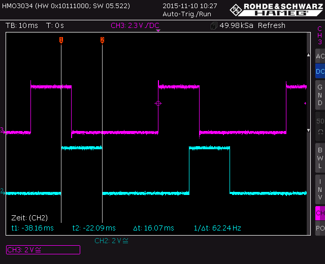
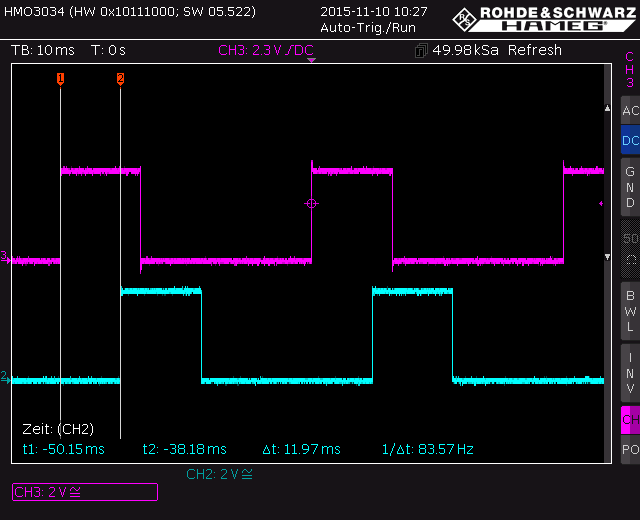
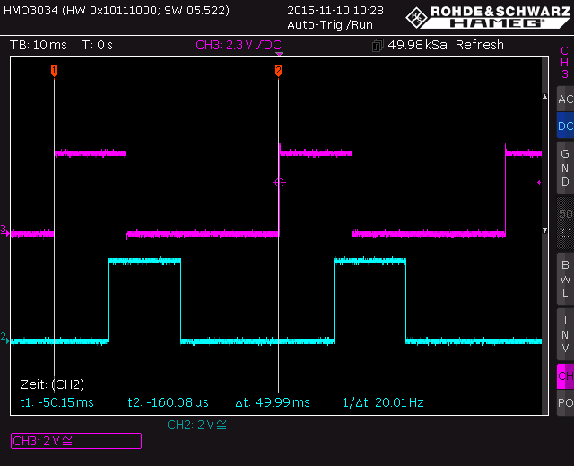
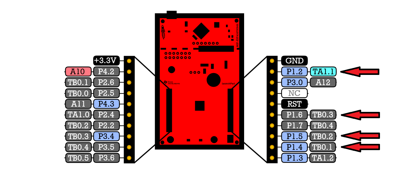
I have a code that generates a PWM. Can someone tell me how to add code to the existing to generate a PWM and give it a delay to certain amount and get that out through one of the ports?

  • Hi Yashaswy!

    Here is some code for you that does the following: The first PWM is on P1.4 (TB0.1) and has a duty-cycle of 16ms. The second PWM on P1.3 (TA1.2) starts 12ms later and also has a duty-cycle of 16ms. Both have a period of 50ms.

    Connect your probes here:

    #FreeSampleCode

    #include <msp430fr5969.h>
    
    
    #define PERIOD  50000                                      // 50ms @ SMCLK = 1MHz
    #define DUTY_CYCLE 16000                                   // 16ms @ SMCLK = 1MHz
    #define DELAY      12000                                   // 12ms @ SMCLK = 1MHz
    
    
    void main( void )
    {
      WDTCTL    =  WDTPW | WDTHOLD;                            // Stop watchdog timer
    
      P1SEL0    =  0x08 | 0x10;                                // Enable timer function for P1.3 (TA1.2) and P1.4 (TB0.1)
      P1DIR     =  0x08 | 0x10;                                // Set P1.3 (TA1.2) and P1.4 (TB0.1) to output direction
      PM5CTL0  &= ~LOCKLPM5;                                   // Disable GPIO power-on default high-impedance mode
    
      CSCTL0_H  =  CSKEY >> 8;                                 // Unlock CS registers
      CSCTL1    =  DCOFSEL_6;                                  // Set DCO = 8MHz
      CSCTL2    =  SELA__VLOCLK | SELS__DCOCLK | SELM__DCOCLK; // Set ACLK = VLOCLK, SMCLK = MCLK = DCOCLK
      CSCTL3    =  DIVS__8 | DIVM__8;                          // Set SMCLK and MCLK divider to 8 -> 1MHz
      CSCTL0_H  =  0;                                          // Lock CS registers
    
      TB0CCR0   =  PERIOD - 1;                                 // Period for 1st PWM
      TB0CCR1   =  DUTY_CYCLE;                                 // Duty cycle for 1st PWM
      TB0CCR2   =  DELAY;                                      // Delay to start 2nd PWM
      TB0CCTL1  =  OUTMOD_7;                                   // TB0.1 reset/set mode (P1.4)
      TB0CCTL2  =  CCIE;                                       // Compare interrupt for 12ms delay
    
      TA1CCR0   =  PERIOD - 1;                                 // Period for 2nd PWM
      TA1CCR2   =  DUTY_CYCLE;                                 // Duty cycle for 2nd PWM
      TA1CCTL2  =  OUTMOD_7;                                   // TA1.2 reset/set mode (P1.3)
    
      TB0CTL    =  TBSSEL_2 | ID_0 | MC_1 | TBCLR;             // 1st PWM: SMCLK, divider 1, up-mode, clear
    
      __bis_SR_register( GIE );                                // Enable interrupts
    
      while( 1 );                                              // Endless loop
    }
    
    
    #pragma vector = TIMER0_B1_VECTOR
    __interrupt void TIMER0_B1_ISR( void )
    {
      TA1CTL   = TASSEL_2 | ID_0 | MC_1 | TACLR;               // 2nd PWM: SMCLK, divider 1, up-mode, clear
      TB0CCTL2 = 0x00;                                         // Clear compare interrupt - executed only once
    }

    P1.4 (TB0.1) is the purple line, P1.3 (TA1.2) is the blue one:

    Have fun!

    Dennis

  • OCY,

    As I mentioned I added other two pulses from Timer_0_B that are expected to start and end at same time. The oscilloscope has 4 probes, so 4 pulses with 2 starting at same time and other 2 with an offset to each other. Also when I'm checking the probes, P1.4 and P1.5 are giving correct output but P1.2 and P1.0 are not able to. This is the modified code. Please find out what I'm missing here. Thank you :)

    #include <msp430.h>

    int main(void)
    {
    WDTCTL = WDTPW | WDTHOLD; // Stop WDT
    // Cofigure GPIO
    P1DIR = BIT2 | BIT0;
    P1SEL0 = BIT2 | BIT0;

    P1DIR = BIT4 | BIT5;
    P1SEL0 = BIT4 | BIT5;

    PM5CTL0 &= ~LOCKLPM5;

    CSCTL0_H = CSKEY >> 8; // Unlock CS registers
    CSCTL1 = DCOFSEL_6; // Set DCO = 8MHz
    CSCTL2 = SELA__VLOCLK | SELS__DCOCLK | SELM__DCOCLK;// Set ACLK=VLO SMCLK=DCO
    CSCTL3 = DIVA__8 | DIVS__8 | DIVM__8; // Set all dividers
    CSCTL0_H = 0; // Lock CS registers


    TA0CCR0 = 16000-1;
    TA0CCR1 = 20;
    TA0CCR2 = 12000-1;

    TA0CCTL1 = OUTMOD_7;
    TA0CCTL2 = CCIE;
    TA0CTL = TASSEL_2 | ID_0 | MC_1 | TACLR;

    TA1CCR0 = 16000-1;
    TA1CCR1 = 20;
    TA1CCTL1 = OUTMOD_7;
    TA1CTL = TASSEL__SMCLK | MC__UP | TACLR; // SMCLK, up mode, clear TAR


    TB0CCR0 = 4000-1;
    TB0CCTL1 = OUTMOD_7; // CCR1 reset/set
    TB0CCR1= 20;


    TB0CCTL2 = OUTMOD_7; // CCR1 reset/set
    TB0CCR2 = 20; // CCR2 PWM duty cycle
    TB0CTL = TBSSEL__SMCLK | MC__UP | TBCLR; // SMCLK, up mode, clear TBR


    __bis_SR_register(GIE); // Enter LPM0
    __no_operation(); // For debugger
    while (1);
    }

    #pragma vector = TIMER0_A1_VECTOR
    __interrupt void TIMER0_A1_ISR( void )
    {
    TA1CTL = TASSEL_2 | ID_0 | MC_1 | TACLR;
    TA0CCTL2 = 0x00;
    }

  • Dennis,
    This is a very good idea. Thank you so much for investing your time to guide me :) . Now I am to add two more pulses which are coming from P1.4 and P1.5 so I am not supposed to use Timer B 0. Coming to the Timer_A_0, I've applied both of them into the same code which I've pasted. Please check why all the four pulses aren't coming together at once.

    Regards,
    Yashaswy
  • Yashaswy, again one can only guess what you want to do...:-\

    At the moment your PWMs seem to be the following:

    // Timer A0
    TA0CCR0  = 16000 - 1;                      // Period of 16ms
    TA0CCR1  = 20;                             // Duty cycle for TA0.1 of 20µs
    
    TA0CCTL1 = OUTMOD_7;                       // Reset/set TA0CCR1
    TA0CTL   = TASSEL_2 | ID_0 | MC_1 | TACLR; // TA0: SMCLK, divider 1, up mode, clear
    
    
    // Timer A1
    TA1CCR0  = 16000 - 1;                      // Period of 16ms
    TA1CCR1  = 20;                             // Duty cycle for TA1.1 of 20µs
    
    TA1CCTL1 = OUTMOD_7;                       // Reset/set  TA1CCR1
    TA1CTL   = TASSEL__SMCLK | MC__UP | TACLR; // TA1: SMCLK, divider 1, up mode, clear
    
    
    // Timer B0
    TB0CCR0  = 4000 - 1;                       // Period of 4ms
    TB0CCR1  = 20;                             // Duty cycle for TB0.1 of 20µs
    TB0CCR2  = 20;                             // Duty cycle for TB0.2 of 20µs
    
    TB0CCTL1 = OUTMOD_7;                       // Reset/set TB0CCR1
    TB0CCTL2 = OUTMOD_7;                       // Reset/set TB0CCR2
    TB0CTL   = TBSSEL__SMCLK | MC__UP | TBCLR; // TB0: SMCLK, divider 1, up mode, clear

    Are these the desired times for your PWMs?

    Dennis

  • Yeah exactly the same Dennis.. The pulse from Timer A0 and A1 are both have time period of 16ms with a duty cycle of 20us and the pulses from Timer B 0 have a period of 4ms with 20us as the duty cycle.


    Regards,
    Yashaswy

  • Yashaswy Akella said:
    . Also when I'm checking the probes, P1.4 and P1.5 are giving correct output but P1.2 and P1.0 are not able to. This is the modified code. Please find out what I'm missing here. Thank you :)

    If you remove your modification, P1.0 and P1.2 will work.

    It is your modifications that killed P1.0 and P1.2

  • OCY,
    But I want the four pulses which is the final desired output. These both bits of the code are working in different controllers but when given to one single controller they are not able. Please help me this one last time :)

    Regards,
    Yashaswy
  • Yashaswy Akella said:
    Please help me this one last time :)

    Do you mean you are not going to attempt writing program any more for the rest of your life? If so, I will write this one for you. Otherwise you really need to learn how to write and debug program yourself.

  • OCY,
    I love coding. It's just that I'm not able to and the deadline is approaching. This controller was specified and I need help. I agree writing that 'one last time' was my fault. I'm sorry for that. Please help.

    Regards,

    Yashaswy

  • Can you please help me debug the code. As I tried till now and I'm not able to get the logic why the outputs from both P1.0 and P1.2 are not coming.

    Regards,
    Yashaswy
  • Have a look at this part of your code - the error is located in here:

    // Cofigure GPIO
    P1DIR  = BIT2 | BIT0;
    P1SEL0 = BIT2 | BIT0;
    
    P1DIR  = BIT4 | BIT5;
    P1SEL0 = BIT4 | BIT5;

  • Dennis,
    Thank you so much Dennis, now I get it. I'm defining the ports P1.0 and P1.2 and later redefining the output to 1.4 and 1.5. Right?

    P1DIR = BIT2 | BIT0 | BIT4 | BIT5;
    P1SEL0 = BIT2 | BIT0 | BIT4 | BIT5;

    Maybe this works.

    Regards,
    Yashaswy
  • I wouldn't call it "define", but yes, you are overriding your previous made settings for P1SEL0 and P1DIR.

    This would have been another option with the existing code:

    // Cofigure GPIO
    P1DIR   = BIT2 | BIT0;
    P1SEL0  = BIT2 | BIT0;
    
    P1DIR  |= BIT4 | BIT5;
    P1SEL0 |= BIT4 | BIT5;

    Dennis

  • Thank you so much Dennis, this is working and I'm getting the respective pulses.

    Another thing struck me. The pulse from P1.4 (yellow) and the pulse from P1.2 (green) are not starting at the same time - I mean, both of them have the same Duty cycle but have a phase shift. Is there a way to correct that and get the pulses start at the same time?

    Regards,

    Yashaswy 

  • This happens because one is Timer A1 and the other is Timer B0. And since you cannot start them simultaneously, there will always be a phase shift between them. But why do you want to use different timers for the same signal output? If you want to start them almost simultaneously, you could enable TAIE of one timer and start the other one inside the ISR - by doing so, you would wait for one complete cycle of the first one, starting the second timer when the next cycle begins. There will still be a minimal shift, but only a few clock cycles.
  • Thanks for the info Dennis. I missed telling you that the output will have four pulses, three of them starting at the same time and the 4th one having a delay compared to other three (these three will be having different duty cycles). As you mentioned an idea that will work but is that shift inevitable?

    If yes, I have an alternate idea, tell me if its possible. Can I get the output which I'm getting from Timer B 0 through Timer A1 by using any of the other ports - This leaves us only P1.6

    Regards,
    Yashaswy
  • You can get rid of the shift by using the same timebase for the different PWMs, means one timer module. Timer B0 has 0.1, 0.2, 0.3, 0.4 and 0.5 routed out on the LaunchPad. You can use them instead of all the different timers you are using now. Of course not for the one that has the delay and only if the different PWM timings can all be serviced by one timebase.

  • When I first wrote the code for four pulses (of course without the delay) They were starting at the same time. Can you help me modify this snippet as per your suggestion

    P1DIR |= BIT2 | BIT3 | BIT4 | BIT5 ;
    P1SEL0 |= BIT2 |BIT3 | BIT4 | BIT5;


    TA1CCR0 = 16000-1;
    TA1CCTL1 = OUTMOD_7; // CCR2 reset/set
    TA1CCR1 = 20; // CCR1 PWM duty cycle
    TA1CCTL2 = OUTMOD_7; // CCR2 reset/set
    TA1CCR2 = 20;

    TB0CCR0 = 4000-1;
    TB0CCTL1 = OUTMOD_7; // CCR1 reset/set
    TB0CCR1= 20;
    TB0CCTL2 = OUTMOD_7; // CCR1 reset/set
    TB0CCR2 = 20; // CCR2 PWM duty cycle

    Regards,
    Yashaswy
  • What would be your own idea regarding the necessary changes?

  • TB0CCTL3 = OUTMOD_7; // CCR1 reset/set
    TB0CCR3 = 20; // CCR2 PWM duty cycle

    can be an option. But I dont know which port get's it out. I also need the time period as 16ms.

    One question is they were in sync in the code I sent above. I dont understand, how they skipped being in sync in the modified code
  • Yashaswy Akella said:
    TB0CCTL3 = OUTMOD_7; // CCR1 reset/set
    TB0CCR3 = 20; // CCR2 PWM duty cycle

    Both comments do not match the code lines you have written.

  • Changed it..
    TB0CCR3 = 20; // CCR3 PWM duty cycle
  • Simply change your program to only use Timer B0 for the other PWMs than the delayed one.
  • Dennis,
    I've tried changing the positions in the code, It is making getting those pulses together but not starting and ending at the same time
  • I've thought the same but the time period is different compared to others. This makes it more challenging.
  • So you now have three PWMs running from Timer B0 and the fourth (delayed) one from another timer?
  • Only two of them but delay is not coming into effect in this. I mean when I'm changing the delay value as 12ms and 10ms there is no effect on the pulse
  • Use TB0.0 as timebase and TB0.1, 0.2 and 0.3 as duty-cycle for three PWMs with OUTMOD_7. Then use TB0.4 with CCIE and set the CCR register to the delay time you want. Inside the ISR disable the CCIE for TB0.4 and start another timer like TA1 with TA1.0 as timebase and TA1.1 as PWM with OUTMOD_7.

    That's it.
  • One quick question. Now we are getting output out of P1.0 right! Can we get the output out of some other port like P1.3 by defining a statement like 'Output from P1.0 must go to P1.3 ' because holding the probe there at P1.0 is very difficult.

    I've tried fixing it as per your first suggestion, I'm getting very little shift between both of them(the shift is very small but its okay)

    Regards,
    Yashaswy
  • Yashaswy Akella said:
    Can we get the output out of some other port like P1.3 by defining a statement like 'Output from P1.0 must go to P1.3 '

    No. Not when using hardware PWM. You can change the output to pins that support the same timer function. For example TB0.1 is available at P2.6 and P1.4, same for other timer outputs. But you cannot choose completely free where to output the signal.

    But if you would do it like mentiod here...

    Dennis Eichmann said:
    Use TB0.0 as timebase and TB0.1, 0.2 and 0.3 as duty-cycle for three PWMs with OUTMOD_7. Then use TB0.4 with CCIE and set the CCR register to the delay time you want. Inside the ISR disable the CCIE for TB0.4 and start another timer like TA1 with TA1.0 as timebase and TA1.1 as PWM with OUTMOD_7.

    ...then all outputs are easy accessible:

  • Thank you so much Dennis. I'll work on this and get back

    Regards,
    Yashaswy
  • Hi Yashaswy!

    Did you get it running as expected?

    Dennis

**Attention** This is a public forum