This thread has been locked.

If you have a related question, please click the "Ask a related question" button in the top right corner. The newly created question will be automatically linked to this question.

CCS/MSP430FR5969: more details about the S&H circuit

Part Number: MSP430FR5969


Tool/software: Code Composer Studio

Dear colleagues,

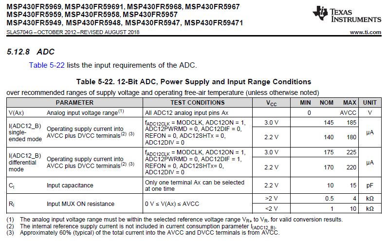
I was wondering if someone has more details about the sample and hold (S&H) circuit of the embedded ADC.

I suppose that the S&H has a switch to do the sampling and a capacitor to hold the voltage. How much are the on-resistance of this switch and the holding capacitance? In the datasheet, the only values specified are the MUX-on resistance and the input capacitance. Maybe the same “switch” of the MUX is employed to do the sampling, and the input capacitance behaves as a holding capacitance. Is that possible?

Best regards!

Ferran

  • Sampling cycle can be set by ADCCTL0.ADCSHTx. Conversion cycle is N+2 (N is resolution number).
    The time of one cycle is Approximately Tau *RC.
    RC is depended on the internal RC and the external RC
    The Approximately Tau is depend on ADC voltage and required for an error of less than ±0.5 LSB
  • Dear Xiaodong,

    Many thanks for your reply! Your explanation is clear, but it does not solve my question.

    As for the internal RC, the R is the MUX on-resistance and C is the input capacitance; this is according to the datasheet and the application notes.

    My point is about the effects of the on-resistance of the switch of the S&H and the ensuing holding capacitor. This is not another internal RC, but nothing is said about that, why?

    Best regards,

    Ferran

  • Hello Xiaodong.

    how do you define Tau?
    Why Tau depends on ADC voltage?
  • Sorry to be late!
    Approximately ten Tau (τ) are needed to get an error of less than ±0.5 LSB: tsample = ln(2n+2) x (RS + RI) x (CI + Cpext), where n = ADC
    resolution = 12, RS= external source resistance, Cpext = external parasitic capacitance.
    my understanding is Tau is the number of RC
    you can find some information www.ti.com/.../msp430fr5994.pdf
    I remember there is one application notes on MSP ADC on TI.COM
    I will find it out and reply later
  • Thanks for reply!
    So not ADC voltage but ADC resolution, agreed.
    I appreciate a MSP ADC app. note.
  • All,

    the FR5xx users guide has some nice explanations on sampling time and internal circuits:

    Together with the FR5969 datasheet parameters you should have all the information you need this principle applies to all ADCs:

    With you have everything you can calculate the required sampling time but for sure you need to know your external circuitry.

    You have to allow the sampling cap to be charged long enough to have a stable voltage. Otherwise you sample the ringing. Imagine you have high external resistance on the point you want to measure. This means it takes some time until the current trough this high resistance path charged the sampling cap and this is the time you need to set up with the sampling timer (number of sampling clocks x selected frequency) for sampling. And exactly this is explained in the users guide.

    Hope this helps!

  • Dear Dietmar,
    Thanks for the reply. Your explanation is clear.
    My doubt is not about how to calculate the sampling time for a given circuit, but it is about which capacitance is employed as a sampling cap. Taking into account the data provided in the datasheet, it seems that the input capacitance (10 pF) is used as a sampling cap. I thought, maybe I am wrong, that after the MUX there was a sample and hold circuit with its own holding capacitor, which is not specified (or this is the 10 pF??)
    Maybe this is not important to estimate the sampling time, but it is to understand how the MUX, S&H and ADC operate.
    Many thanks!!
    Ferran
  • Ferran,

    you understanding is correct the Ci which is max 15 pF is the sampling capacitance including all the parastics from bonding, pad and switches and this is what is important for correct ADC ussage. And this is the only value which is important to estimate the sampling time. Otherwise we need to seperate all the values which would not have a benefit for our customers.

    Hope this helps.
  • Many thanks!
    I thought that the holding capacitance of a S&H circuit was higher than a few pF, say some nF.
    On the other hand, the internal resistance specified is the on-resistance of the MUX. This means that the "switch" of the MUX also carries out the typical sampling function of the S&H circuit?
  • Ferran,

    I checked the design and there is nothing in the nF range implemented so please take the 15pF max value. I mean the MUX it self is the only "barrier" or resistive path to the samplign cap that's why it mainly contributes to this.
    So you can imagine that this complex ultra lower power ADC architectures does not only consist of a simple switch and a simple cap. Everything is aligned to lowest power and performance. Because this is TI IP details on the architecture are not disclosed which makes no sense at all for the proper ussage. For using the ADC all important parameters are specified and published. The user guide describes that it is a SAR based ADC and how this works can be found in the literature. I hope this helps to answer all your questions.
  • Dietmar, thanks!

    ln(2n+2) and ln(2pow(n+2)) makes a difference.

**Attention** This is a public forum