This thread has been locked.

If you have a related question, please click the "Ask a related question" button in the top right corner. The newly created question will be automatically linked to this question.

SPI problem with TI Launchpad + MCP2515 Can Controller

Other Parts Discussed in Thread: MSP430G2553

Hi, so I designed a simple circuit board that fits on top of the Launchpad. This circuit board has the MCP2515 Can Controller, SN65HVD TI Can Transceiver, and some other basic circuit components.

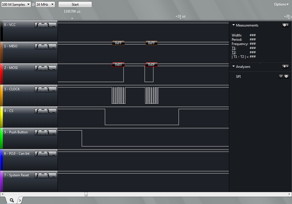
All I am focusing on right now is the SPI. The issue that I am having is that the MISO (master in slave out) line is always logic high. The other lines, SCK, MOSI, STE, all work fine.

I wrote a simple program for the Launchpad that, upon pushing the P1.3 button, sends a "Read Register" instruction to the MCP2515. This instruction is then sent a second time, and that is the end of the program.

All communication lines are fine, except for MISO, which is stuck at logic high. After lots of playing around, I ran into a situation where the MISO line went low for a very short instant (~40 ns), and then back to high.

Attached to this post are a picture of the schematic of my circuit board (R4 not connected), two pictures showing the waveform that I got from the Logic Analyzer, and printed below is the code that I used.

I appreciate any help that I can get and I am happy to provide any additional information or clarifications that may be needed.

Thank You.

#include "msp430g2553.h"
unsigned char step;
void main(void){
WDTCTL = WDTPW + WDTHOLD;               // Stop watchdog timer
P1DIR = BIT0 + BIT5 + BIT6; // LEDs and STE output
P1SEL = BIT1 + BIT2 + BIT4;
P1SEL2 = BIT1 + BIT2 + BIT4;
UCA0CTL0 = UCMSB + UCMST + UCSYNC + UCCKPH + UCMODE_0;
UCA0CTL1 |= UCSSEL_2;                   // SMCLK
UCA0BR0 = BIT1 + BIT0;                  // /3
UCA0BR1 = 0;                            //
UCA0MCTL = 0;                           // No modulation
UCA0CTL1 &= ~UCSWRST;                   // **Initialize USCI state machine**
IE2 |= UCA0RXIE;             // Enable USCI0 RX interrupt
DCOCTL = BIT7 + BIT6 + BIT5; //clock is ~6-8MHz
BCSCTL1 = BIT3 + BIT2 + BIT1 + BIT0;
//push button settings (P1.3)
P1REN = BIT3;                       // P1.3 pullup
P1IE |= BIT3;                       // P1.3 interrupt enabled
P1IFG &= ~BIT3;                     // P1.3 IFG cleared
P1IES |= BIT3;                     // P1.3 Hi/lo edge
P1OUT |=  BIT3;                       // P1.3 set, else reset
P1OUT &= ~BIT0; //red LED off
P1OUT &= ~BIT6; //green LED off
P1OUT |= BIT5; //STE high
step = 0; //variable for testing SPI
__bis_SR_register(LPM0_bits + GIE);     // CPU off, enable interrupts
}
//Push Button ISR
#pragma vector=PORT1_VECTOR
__interrupt void Port_1(void)
{
P1IFG &= ~BIT3;                 // P1.3 IFG cleared
IFG2 |= BIT0; // cause RX interrupt
}
//RX ISR
#pragma vector=USCIAB0RX_VECTOR
__interrupt void USCIA0RX_ISR(void)
{
switch(step){
case 0x0:
P1OUT &= ~BIT5; // lower STE
UCA0TXBUF = 0x3; // "Read" Instruction
step++;
case 0x1:
UCA0TXBUF = 0xF; // "Read" address, CANCTRL reg.
__delay_cycles(50);
P1OUT |= BIT5; // raise STE
step++;
case 0x2:
__delay_cycles(50);
P1OUT &= ~BIT5; // lower STE
UCA0TXBUF = 0x3; // "Read" Instruction
step++;
case 0x3:
UCA0TXBUF = 0xF; // "Read" address, CANCTRL reg.
__delay_cycles(50);
P1OUT |= BIT5; // raise STE
step++;
default:
IFG2 &= ~BIT0; // clear interrupt
} // THE END
}
  • p450 of the user guide states that you should set the UCSWRST bit before fiddling with the UCS registers. But it is set on power up so you can be let off on this one.  ;)

    Disconnect your circuit from launch pad and connect MISO to MOSI. Then re run the test with the logic analyzer connected.   

  • Seth Berggren said:
    The issue that I am having is that the MISO (master in slave out) line is always logic high. The other lines, SCK, MOSI, STE, all work fine.

    So the slave doesn't send anything. Nothing that is controlled by MSP code.

    Seth Berggren said:
    P1OUT |= BIT5; //STE high

    Well, P1.5 isn't STE. This name is only used for USCI slave/multi master operation adn input only.
    You use this pin as normal GPIO for providing teh chip select signal for the slave, so "CS" would be more appropriate and less confusing. Note that there can be as many different CS signals as there are different slaves on the SPI bus.

    But I wonder how your code shall work.

    SPI is give-and-take. After releasing SWRST, UCA0TXIFG is set and UCA0RXIFG is clear. So your RX ISR won't be called unleyy sou actually write something into TXBUF, which in turn creates a transfer. Well, your manual setting of RXIFG in the port ISR is - surprising. But it does the job.
    However, then things get strange.
    Your RX ISR goes into case 1, where you lower teh slave chip select. Some slaves require a minimum delay after that. Then you write to TXBUF which sends the first byte. But  at this point, you should break out of the case, clear the RXIFG bit and exit the ISR. Instead you proceed right to the next case (while the SPI hasn't sent a bit yet), stuff another byte into TXBUF, do some busy-waiting cycles (a no-go inside an ISR) and never read RXBUF at all.
    This code doesn't need a switch/case structure and doesn't belong into an ISR at all.

    However, a close look on the screenshots shows that the occasional low pulse of your slave comes at the last falling edge of teh clock signal. Which isn't a valid position at all.

    So besides the coding oddity I'd say you picked the wrong polarity/phase for the clock. Usually, the clock is low-active (idle-high), which requires the CKPL bit set. And in most cases, CKPH doesn't need to be set or the slave will listen to and push data out on the wrong clock edge.

    p.s.: the Saleae analyzer is a very good device. Especially the software is excellent.

  • Thanks for the reply Jens,

    I took most of your advice. I got rid of the delay cycles in the ISR and set the SPI mode of the MSP430 to 1,1 (the MCP2515 accepts 0,0 or 1,1 mode SPI). The only issue I ran into with changing the SPI was that, when I loaded the bytes 0x03 and 0x0F into the TX buffers, the analyzer kept reading them as 0x07 and 0x1F. I figured it is just a timing thing with the bits, so instead I sent the bytes 0x01 and 0x07, and the analyzer reads the correct bytes now.

    Still, after making those changes, the MISO line is unresponsive.

    I think my next step is to switch the MISO and MOSI lines, as suggested earlier, although I doubt that is the problem... Do you have any other suggestions that might help me out here?

    Thank You.

    Here is my new code, and below that is the new waveforms that I produced:

    #include "msp430g2553.h"
    unsigned char step;
    void main(void){
    WDTCTL = WDTPW + WDTHOLD;               // Stop watchdog timer
    P1DIR = BIT0 + BIT5 + BIT6; // LEDs and CS output
    P1SEL = BIT1 + BIT2 + BIT4;
    P1SEL2 = BIT1 + BIT2 + BIT4;
    UCA0CTL0 = UCMSB + UCMST + UCSYNC + UCCKPL + UCCKPH + UCMODE_0;
    UCA0CTL1 |= UCSSEL_2;                   // SMCLK
    UCA0BR0 = BIT1 + BIT0;                  // /3
    UCA0BR1 = 0;                            //
    UCA0MCTL = 0;                           // No modulation
    UCA0CTL1 &= ~UCSWRST;                   // **Initialize USCI state machine**
    IE2 |= UCA0RXIE;             // Enable USCI0 RX interrupt
    DCOCTL = BIT7 + BIT6 + BIT5; //clock is ~6-8MHz
    BCSCTL1 = BIT3 + BIT2 + BIT1 + BIT0;
    //push button settings (P1.3)
    P1REN = BIT3;                       // P1.3 pullup
    P1IE |= BIT3;                       // P1.3 interrupt enabled
    P1IFG &= ~BIT3;                     // P1.3 IFG cleared
    P1IES |= BIT3;                     // P1.3 Hi/lo edge
    P1OUT |=  BIT3;                       // P1.3 set, else reset
    P1OUT |= BIT5; //CS high
    step = 0; //variable for switch case
    __bis_SR_register(LPM0_bits + GIE);     // CPU off, enable interrupts
    }
    //Push Button ISR
    #pragma vector=PORT1_VECTOR
    __interrupt void Port_1(void)
    {
    P1IFG &= ~BIT3;                 // P1.3 IFG cleared
    IFG2 |= BIT0; // cause RX interrupt
    }
    //RX ISR
    #pragma vector=USCIAB0RX_VECTOR
    __interrupt void USCIA0RX_ISR(void)
    {
    IFG2 &= ~BIT0; // clear RX IFG
    P1OUT &= ~BIT5; // lower CS
    switch(step){
    case 0x0:
    UCA0TXBUF = 0x1; // "Read" Instruction
    step++;
    break;
    case 0x1:
    UCA0TXBUF = 0x7; // "Read" address, CANCTRL reg.
    step++;
    break;
    case 0x2:
    P1OUT |= BIT5; // raise CS
    step = 0x0; // restart sequence by pushing button
    break;
    }
    }


  • Seth Berggren said:
    (the MCP2515 accepts 0,0 or 1,1 mode SPI)

    Well, Motorola mode 0,0 isn't TI mode 0,0. The clock polarity is reversed between the two. So I think on the MSP you'll need mode 1,0 to serve Motorola mode 0.0

    About your signals: well, I don't know the high-level protocol of your slave.

    It's possible that while you send the first byte, teh slave simply han't anythign to say (remember, it hasn't received your first byte yet adn therefore cannto send any answer, so it probably just sends an 0xff dummy).

    If the two bytes you send form a command, you'll be required to send a third dummy byte (probably 0xff) to allow the slave sending an answer. When CS goes high, this cancels the high-level protocol and the slave won't send an answer to the previous request on your next attempt.

    This would also explain the sputious blip you encountered on MISO: the slave took the last clock edge (due to wrong polarity(phase) as the beginning of a third byte and started to send its answer - which then was canceled because no more clock cycles were coming and then CS was going high again.

**Attention** This is a public forum