This thread has been locked.

If you have a related question, please click the "Ask a related question" button in the top right corner. The newly created question will be automatically linked to this question.

Spy-Bi Wire and JTAG Interfacing

Dear Sir,

                  I have Some doubts on MSP430G2 Launch pad Spy-Bi wire and MSP-FET430UIF Spy-Bi wire, Both of these interface’s are doing same work

1. what are the difference between MSP430G2 Launch Pad Spy-Bi wire Interfacing and JTAG or MSP-FET430UIF
Interfacing.

2. and here I have Inserted two of the MSp430 Interfacing Images.

I know this much about These two interfacer.

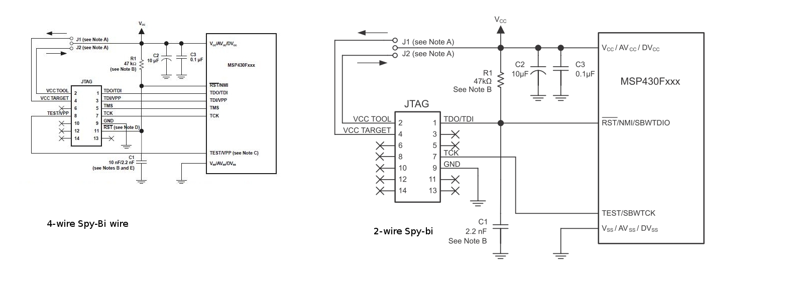
In JTAG Interfacing following pins connecting to MSP430 External IC

JTAG Pins    MSP430 pins
TDO               -   P1.7
TDI                 -   P1.6
TMS               -   P1.5
TCK                -   P1.4
RESET
TEST
VCC
GND

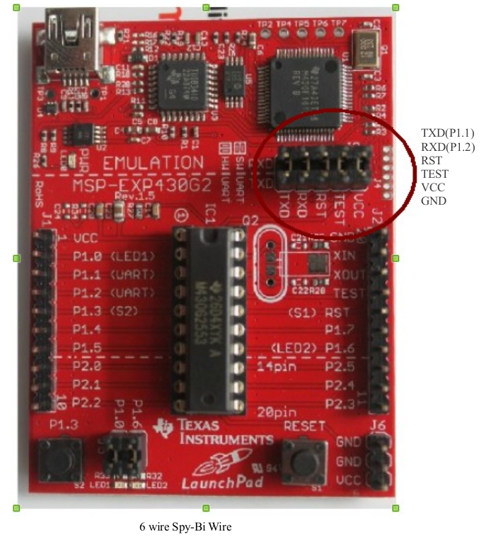
In MSP430G2 Launch Pad Spy-Bi wire following pins connecting to MSP430 External IC

Spy-Bi            MSP430 pins

RXD                       P1.1

TXD                       P1.2  

RESET

TEST
VCC
GND

If any mistakes Please sorry.

Thank you.

  • Hi Mallappa,

     what are the difference between MSP430G2 Launch Pad Spy-Bi wire Interfacing and JTAG or MSP-FET430UIF
    Interfacing.

    Like you mentioned above, JTAG uses 4 (or 5, for RESET) pins and is used for debugging and testing an IC. However, it can also be used to program to the MCU these days.

    Spy-Bi-Wire is a serialized JTAG protocol developed by TI for programming the MSP430 MCUs. It uses only two pins, namely, the RST and TEST pins for data, along with the power pins VCC and GND.

    Please note that  Spy-Bi-Wire doesn't use the RXD and TXD pins, as in the table you have drawn.
    (RXD and TXD are used by the USCI/USI of the MSP430 for features like UART,SPI,etc communications)

    Regards


  • Kevin Jerome said:
    Please note that  Spy-Bi-Wire doesn't use the RXD and TXD pins, as in the table you have drawn.
    (RXD and TXD are used by the USCI/USI of the MSP430 for features like UART,SPI,etc communications)

    Almost :)

    The quoted table does not list RX and TX of the USCI module (hardware UART) but rather the pins used by the serial BSL for data transmission. Which are usually the TA0.0 and TA0.1 pins (the BSL uses a timer-based software UART that adapts its timing to the incoming sync byte).

    However, JTAG/SBW controls the CPU and the memory bus through the embedded emulation module (EEM), while the BSL is a program executed by the CPU (before executing the user application and only if requested by a specific entry sequence on RST and TEST pin)

  • Thank you very much for the insight :)
     

**Attention** This is a public forum