This thread has been locked.

If you have a related question, please click the "Ask a related question" button in the top right corner. The newly created question will be automatically linked to this question.

MSP430G2553: I2C hangs but keeps generating CLK signal in communication with BNO055

Part Number: MSP430G2553
Other Parts Discussed in Thread: MSP430WARE

Hello,

I have encountered I2C communication problem that I haven't been able to solve for a while.

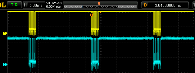
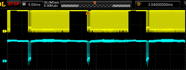
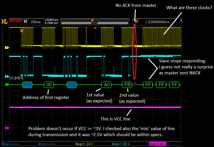
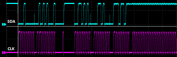
I am using MSP430g2553 to communicate with Bosch BNO055 sensor using their provided C library. In normal conditions I can set up the sensor and read the required data - communication is working fine. However, if the supply voltage of sensor node (for both MSP and BNO055) drops, then starting around 3V at a random time BNO055 often fails to respond and the I2C communication hangs. Weird part is that the MSP430G2553 keeps generating CLK signal seemingly forever (see attached wave forms) while the code has hanged on something like while(!(IFG2 & UCB0RXIFG)) in my I2C subroutine.

I can't figure out:

-why MSP keeps generating CLK when it has hanged on a single code line?

-why the BNO055 stops responding in the first palce?

I implemented kind of a guard timer that resets the communication after some timeout interval so the code at least doesn't hang completely, however, if the supply voltage is <3V (but still within specs of both MSP and BNO055) then most of the time I can read only couple of bytes till this happens.

In my application I am interested in running the sensor node on as low supply voltage as possible as I need to power it along relatively long power supply lines that introduce voltage drop. However, even around 3V I start to get problems and if dropping lower communication fails most of the time making continuous data stream impossible.

Any help in understanding the behavior of MSP and/or BNO055 would be greatly appreciated.

Thank you in advance,

Atis

P.S. I have checked with oscilloscope power supply line and it doesn't seem to have any sudden drops when the problem occurs. I'm also aware of the BNO055 clock stretching - its annoying, but doesn't seem to cause the problem.

  • Hi Atis, 

    Thanks for providing a detailed description of the issue you're experiencing along with screenshots. 

    First I'd like to point you to the Solutions to Common eUSCI and USCI Serial Communication Issues on MSP430 MCUs application report. Please read through the I2C section to see if your problem may be addressed there. 

    Next, you mentioned that things start to get strange at ~3V, does communication always work as expected above 3V? I would take a look at your pull-up resistors and ensure that they are within I2C spec. 

    To address you specific questions:

    1. why MSP keeps generating CLK when it has hanged on a single code line?
      1. The MSP430 is generating a clock and waiting for a response from the BNO055 that never arrives
      2. The MSP will continue to generate this until either data is received or a user implemented timeout stops the module
    2. why the BNO055 stops responding in the first palce?
      1. This I can't answer right now. Be sure to look closely at the BNO055 datasheet and ensure you are meeting all the required specifications.

    Finally, could you please provide a simplified code snippet of the issue so I can review your implementation and try to replicate the issue on my end?

    Best regards, 
    Caleb Overbay

  • Hi Caleb,

    Thank you for your answer. I went through the suggested application report and could not find anything that would point out any mistake I could have made.

    Regarding voltage - yes, above 3V communication seems to be fine and reliable. Around 3V occasional errors occur and around 2.9 V and lower most of the read attempts fail. I have tried different pull-up resistors ranging form 10k to 2k and the problem does not seem to be impacted by that. I guess it would be expected as the I2C signal wave forms seems acceptable around that pull-up range. Could I be missing something here?

    1. I wasn't aware that this is normal behavior of MSP430 USCI module. Thank you for clarifying that. However, I don't seem to understand following - how the USCI module knows if the data has been received? As far as I understand for each received byte all it does is send out 8 clock pulses (meanwhile registering answer from slave whatever the value is) and then on 9th pulse it sends either ACK if all is fine or NACK if it wants to terminate communication. How can it know if slave is responding or not?

    2. I can't find anything that gets violated. As the problem seems to occur only for lowered voltages I assume that everything with I2C timing etc. is fine. And the BNO055 datasheet specifies that it should work down to 2.4 V (actually internal uC and I/O should work even down to 1.7 V). Also, even for low voltages normally I can read at least couple of bytes until communication fails.

    Taking into account my considerations from (1.) I actually start to think that the problem is on MSP430 side. Looking at I2C wave forms it seems that in the last byte (read) before the communication hangs the MSP430 doesn't ACK the reception. It looks like it for some reason doesn't detect incoming data, doesn't acknowledge it and then continues to generate CLK.

    I attach I2C data read subroutine that is connected to BNO055 driver library. As you can see in all waiting loops I have added checking of time_out variable which can be set by a timer to ensure that code doesn't hang in case of communication error. The timer overflow sets the 'time_out' variable that essentially aborts the communication and resets USCI module. 

    /* Input:
    	dev_addr - slave I2C address
    	reg_addr - address of the first register to be read
    	*reg_data - pointer to the location where received data will be stored
    	*cnt - number of bytes to be read
    */
    s8 BNO055_I2C_bus_read(u8 dev_addr, u8 reg_addr, u8 *reg_data, u8 cnt){
    	s8 status=0;    //0 = no error
    
    	while((UCB0CTL1 & UCTXSTP) && !time_out); 	   //ensure that previous communication has finished
    	if(time_out){
    		status=-1;
    		return status;
    	}
    
        UCB0I2CSA=dev_addr;										 // Set slave address
    	UCB0CTL1|=UCTR;											 // Set write mode
    	IFG2&=~(UCB0TXIFG+UCB0RXIFG);        					 // Clear transmission/reception flags
    	UCB0CTL1|=UCTXSTT;										 // Send start condition
    	while((!(IFG2 & UCB0TXIFG))&&(!(UCB0STAT & UCNACKIFG))&& !time_out);// wait till TX finished or NACK (slave) or timeout
    	if(time_out){
    			status=-1;
    			return status;
    	}
    
    	IFG2&=~UCB0TXIFG;										// Clear transmission flag
    	if(!(UCB0STAT & UCNACKIFG)){ 							// If we haven't received NACK
    		UCB0TXBUF=reg_addr; 				                // Send register address
    		while((!(IFG2 & UCB0TXIFG))&&(!(UCB0STAT & UCNACKIFG))&& !time_out); //Wait till TX finished or NACK or timeout
    		if(time_out){
    				status=-1;
    				return status;
    		}
    
    
    		if(!(UCB0STAT & UCNACKIFG)){			// If we haven't received NACK
    			IFG2=~(UCB0TXIFG+UCB0RXIFG);		// Clear TX/RX flags
    			UCB0CTL1&=~UCTR;					// Set read mode
    			UCB0STAT&=~UCNACKIFG; 				// clear NACK flag
    			UCB0CTL1|=UCTXSTT; 					// Generate repeated start
    
    			if(cnt==1){   //if only one byte is going to be received
    				while((UCB0CTL1 & UCTXSTT)&& !time_out);  //wait until STT cleared to generate master NACK and then stop condition.
    				if(time_out){
    						status=-1;
    						return status;
    				}
    
    				UCB0CTL1|=UCTXSTP;	// generate master NACK and stop condition
    				if(!(UCB0STAT & UCNACKIFG)){ 				// If we haven't received NACK
    					while(!(IFG2 & UCB0RXIFG)&& !time_out);//wait till RX flag or timeout
    					if(time_out){
    							status=-1;
    							return status;
    					}
    
    					IFG2&=~UCB0RXIFG;    //Clear RX flag
    					*reg_data=UCB0RXBUF; //store received data in address 'reg_data'
    
    					return status; // return no error
    				}
    			}
    			else{		//if more than one byte is going to be received
    				while((!(IFG2 & UCB0RXIFG))&&(!(UCB0STAT & UCNACKIFG))&& !time_out);// wait till RX flag or NACK or timeout
    				if(time_out){
    						status=-1;
    						return status;
    				}
    
    				if(!(UCB0STAT & UCNACKIFG)){  // If we haven't received NACK
    				    u8 i;
    					for(i=0; i<(cnt); i++){
    						while(!(IFG2 & UCB0RXIFG)&& !time_out);//wait till data is received in incoming buffer or timeout
    						if(time_out){
    								status=-1;
    								return status;
    						}
    
    						IFG2&=~UCB0RXIFG;		//Clear reception flag
    						*(reg_data+i)=UCB0RXBUF; //store recieved data into array addres=reg_data+number_of_byte(i).
    						if(i==(cnt-2)){		// After second to last byte set stop condition
    							UCB0CTL1|=UCTXSTP;
    						}
    					}
    
    					return status; // return no error
    				}
    			}
    		}
    	}
    	
    	// If we have received NACK
    	UCB0STAT&=~UCNACKIFG;// clear NACK flag
    	UCB0CTL1|=UCTXSTP;	// generate stop condition
    
    	status=-1;
    	return status; //return error
    }

    Thank you for help,

    Regards,

    Atis

  • Hi Atis,

    I need to correct myself. The MSP430 should not be continuously sending the CLK signal. The snippet you've provided above looks ok but I need to know more about your system to understand why dropping the voltage could cause issues. Could you provide information about the msp430 clock frequency, communication rate, and I2C initialization code.

    I suspect this issue is unrelated to the I2C module/code because it is working fine above 3V. When reducing VCC of the MSP430 you need to be mindful that the supply voltage is still sufficient to run at the desired system frequency. If this is not met, you could see erratic code execution. You can find information on the required voltage for any specific system frequency in the Recommended Operating Conditions section of the devices datasheet.

    Best regards,
    Caleb Overbay
  • Hi Caleb,

    I'm running MSP430 with 8 Mhz and SMCLK 2 MHz. This is initialization code fro CLK system:

    BCSCTL1=CALBC1_8MHZ;
    DCOCTL=CALDCO_8MHZ;
    BCSCTL2|=DIVS_2;    //SMCLK divider = 4;

    I'm running I2C from SMCLK on 400 kHz (I have also tried 200 kHz and 100 kHz, the problem stays the same). I am reading 8 bytes of data (consecutive reads after repeated start) every 20 ms (50Hz data acquisition rate). Here is the I2C initialization:

    /*I2C USCIB0 init*/
    UCB0CTL1|=UCSWRST;               // put module in reset state
    P1SEL|=BIT6+BIT7;
    P1SEL2|=BIT6+BIT7;               // P1.6=SCL (I2C) P1.7=SDA (I2C)
    UCB0CTL1|=UCSSEL_3;              // select SMCLK
    UCB0CTL0|=UCMODE_3+UCMST+UCSYNC; // set I2C MODE MASTER MODE
    UCB0BR0=5;                       // set I2C clock prescaler. 2Mhz/5=400kHz
    UCB0CTL1 &= ~UCSWRST;            // start I2C

    By your advice I checked again MSP430g2553 data sheet (SLAS735J). I belive Recomended Operating Conditions in page 21 Fig. 1. is what you were referring to. As far as I understand to run MCU on 8 Mhz only ~2.3V are required. I2C frequencies are relatively low, so there should not be a problem regarding specific I/O port requirements. Could there be a trap somewhere else?

    Regards,

    Atis

  • Hi Atis,

    Thanks for the additional data. I don't see anything out of the ordinary with the initialization code you've provided above. You mentioned you were using a Bosch library. Could you provide a link to this library or provide your code so I can try to replicate the issue on my end?

    Best regards,
    Caleb Overbay
  • Hi Caleb,

    The BNO055 driver library is available here. It just provides abstraction layer from BNO055 registers but in the end utilizes your own I2C subroutines. However, to take the library out of the equation I tried to read the sensor data directly without calls through the library, for example:

    BNO055_I2C_bus_read(0x28, 0x20, &data_buffer[0], 8);

    The problem still persists.

    As always the error occurs somewhere during transmission (but I get at least one or more bytes) I tried to read the same registers one by one as separate transmissions:

    BNO055_I2C_bus_read(0x28, 0x20, &data_buffer[0], 1);
    BNO055_I2C_bus_read(0x28, 0x21, &data_buffer[1], 1);
    BNO055_I2C_bus_read(0x28, 0x22, &data_buffer[2], 1);
    BNO055_I2C_bus_read(0x28, 0x23, &data_buffer[3], 1);
    BNO055_I2C_bus_read(0x28, 0x24, &data_buffer[4], 1);
    BNO055_I2C_bus_read(0x28, 0x25, &data_buffer[5], 1);
    BNO055_I2C_bus_read(0x28, 0x26, &data_buffer[6], 1);
    BNO055_I2C_bus_read(0x28, 0x27, &data_buffer[7], 1);

    To my surprise I am able to get the data in this way. I tested down to about 2.4 V and could get seemingly reliable data transmission. This is a great advancement, however, I still want to get to the cause of this matter. In this case a big drawback is that you need to send slave I2C and register address for each byte which noticeably increases overhead and limits the sampling interval and amount of data it is possible to get from sensors.

    The the thing that I am able to reliably use my I2C read subroutine when reading a singe byte but not multiple, should point to some error in the part which handles multiple byte reception. However, I don't notice any mistake there. And in context with dependency on supply voltage it gets very strange. Could it be that there are some specific requirements for USCI module when handling multiple I2C reads?

    Regards,

    Atis

  • Hi Atis,

    I'll try to implement this on my end. I'm still struggling to understand the connection between supply voltage effecting multiple I2C reads. I'm curious to see how many consecutive reads can be performed before failure occurs (i.e. trying different values between 1 to 8). I'll keep you updated on this.

    Best regards,
    Caleb Overbay
  • Hi Atis,

    I am having trouble replicating this issue. Would you be able to share the full I2C communication code or your project with us? If you don't want to post the code to the forum, you could send me a private message on E2E with the code.

    Best regards,
    Caleb Overbay
  • Hi Caleb,

    Sorry for delay I was busy with other issues, but finally today found some time to get back to this.

    I manged to strip down all my project to almost bare bones. Got completely rid of BNO055 driver. All the code does now is:

    In initialization:

    -setup MSP clk module

    -setup I2C module

    -setup couple of timers (one for i2c timout, other for sampling rate control)

    In the work loop:

    -read the data from BNO055 sensor and basically do nothing.

    Here is the full code together with initialization and I2C subroutines:

    #include <msp430g2553.h>
    
    /*Function declarations*/
    void init_MSP();
    void InitBNO055();     
    signed char BNO055_I2C_bus_write(u8 dev_addr, u8 reg_addr, u8 *reg_data, u8 cnt);
    signed char BNO055_I2C_bus_read(u8 dev_addr, u8 reg_addr, u8 *reg_data, u8 cnt);
    
    
    /*Global variables*/
    unsigned char data_buffer[8];
    volatile char time_out=0;
    int sync=0;
    
    #pragma vector = TIMER1_A1_VECTOR
    __interrupt void myTimer(void){
    	time_out=1;
    	//TA1CTL&=~MC_3;
    	TA1CTL&=~TAIFG;
    	//UCB0CTL1|=UCTXSTP;
    	UCB0CTL1|=UCSWRST; 			// put module in reset state
    	__delay_cycles(8000);
    	UCB0CTL1 &= ~UCSWRST;  // start I2C
    }
    
    #pragma vector = TIMER0_A1_VECTOR
    __interrupt void Timer_A(void){
    	TA0CTL&= ~TAIFG;
    	sync=1;
    }
    
    /*
     * main.c
     */
    int main(void){
    	WDTCTL = WDTPW | WDTHOLD;	// Stop watch dog timer
    
    	init_MSP();
        __delay_cycles(7000000);    //wait for BNO055 to setup
        InitBNO055();
    
        // program main cycle
    	while(1){
    		while(!sync);
    		sync=0;
    		
    		//RECEIVE DATA HERE:
    		time_out=0;
    		TA1CTL|=TACLR;
    		TA1CTL|=MC_1; // run timer
    
    		//DOES NOT WORK with this:
    		BNO055_I2C_bus_read(0x28, 0x20, &data_buffer[0], 8);
    
    		//DOES WORK with this:
    		/*
    		BNO055_I2C_bus_read(0x28, 0x20, &data_buffer[1], 1);
    		BNO055_I2C_bus_read(0x28, 0x21, &data_buffer[0], 1);
    		BNO055_I2C_bus_read(0x28, 0x22, &data_buffer[3], 1);
    		BNO055_I2C_bus_read(0x28, 0x23, &data_buffer[2], 1);
    		BNO055_I2C_bus_read(0x28, 0x24, &data_buffer[5], 1);
    		BNO055_I2C_bus_read(0x28, 0x25, &data_buffer[4], 1);
    		BNO055_I2C_bus_read(0x28, 0x26, &data_buffer[7], 1);
    		BNO055_I2C_bus_read(0x28, 0x27, &data_buffer[6], 1);
    		*/
    
    		TA1CTL&=~MC_3; //stop timer;
    		time_out=0;
    	}
    }
    
    void init_MSP(){
    	//init clk system
    	BCSCTL1=CALBC1_8MHZ;
    	DCOCTL=CALDCO_8MHZ;
    	BCSCTL2|=DIVS_2;    //SMCLK divider = 4;
    
    	/*I2C USCIB0*/
    	UCB0CTL1|=UCSWRST; 			// put module in reset state
    	P1SEL|=BIT6+BIT7;
    	P1SEL2|=BIT6+BIT7;			// P1.6=SCL (I2C) P1.7=SDA (I2C)
    	UCB0CTL1|=UCSSEL_3; 		// select SMCLK
    	UCB0CTL0|=UCMODE_3+UCMST+UCSYNC; 	// set I2C MODE MASTER MODE
    	UCB0BR0=20; 		   // clk divider from SMCLK
    	UCB0CTL1 &= ~UCSWRST;  // start I2C
    
    	// setup timer for i2c timout
    	TA1CTL=TASSEL_2+ID_0+TAIE;			//SMCLK; no divider; Timer interupt on
    	TA1CCR0=28000;					//i2c communication timout
    
    	// setup timer for sampling rate control
    	TA0CTL=TASSEL_2+ID_0+TAIE;			//SMCLK; no divider; Timer interupt on
    	TA0CCR0=40000;					    //50 Hz sampling rate
    	TA0CTL|=MC_1; // run sampling rate control timer
    
    	_enable_interrupts();
    }
    
    void InitBNO055(){
        //BNO055 SETUP 
        u8 data_to_write=0x80;    
        BNO055_I2C_bus_write(BNO055_I2C_ADDR1, 0x3F, &data_to_write, 1);   //Enable external oscilator:
        data_to_write=0x0C;
        BNO055_I2C_bus_write(BNO055_I2C_ADDR1, 0x3D, &data_to_write, 1);   //NDOF mode
    }
    
    
    //-----------BNO055 I2C DRIVER FUNCTIONS-----------------------
    /* Input:
        dev_addr - slave I2C address
        reg_addr - address of the first register to be read
        *reg_data - pointer to the location where received data will be stored
        *cnt - number of bytes to be read
    */
    s8 BNO055_I2C_bus_read(u8 dev_addr, u8 reg_addr, u8 *reg_data, u8 cnt){
        s8 status=0;    //0 = no error
    
        while((UCB0CTL1 & UCTXSTP) && !time_out);      //ensure that previous communication has finished
        if(time_out){
            status=-1;
            return status;
        }
    
        UCB0I2CSA=dev_addr;                                      // Set slave address
        UCB0CTL1|=UCTR;                                          // Set write mode
        IFG2&=~(UCB0TXIFG+UCB0RXIFG);                            // Clear transmission/reception flags
        UCB0CTL1|=UCTXSTT;                                       // Send start condition
        while((!(IFG2 & UCB0TXIFG))&&(!(UCB0STAT & UCNACKIFG))&& !time_out);// wait till TX finished or NACK (slave) or timeout
        if(time_out){
                status=-1;
                return status;
        }
    
        IFG2&=~UCB0TXIFG;                                       // Clear transmission flag
        if(!(UCB0STAT & UCNACKIFG)){                            // If we haven't received NACK
            UCB0TXBUF=reg_addr;                                 // Send register address
            while((!(IFG2 & UCB0TXIFG))&&(!(UCB0STAT & UCNACKIFG))&& !time_out); //Wait till TX finished or NACK or timeout
            if(time_out){
                    status=-1;
                    return status;
            }
    
    
            if(!(UCB0STAT & UCNACKIFG)){            // If we haven't received NACK
                IFG2=~(UCB0TXIFG+UCB0RXIFG);        // Clear TX/RX flags
                UCB0CTL1&=~UCTR;                    // Set read mode
                UCB0STAT&=~UCNACKIFG;               // clear NACK flag
                UCB0CTL1|=UCTXSTT;                  // Generate repeated start
    
                if(cnt==1){   //if only one byte is going to be received
                    while((UCB0CTL1 & UCTXSTT)&& !time_out);  //wait until STT cleared to generate master NACK and then stop condition.
                    if(time_out){
                            status=-1;
                            return status;
                    }
    
                    UCB0CTL1|=UCTXSTP;  // generate master NACK and stop condition
                    if(!(UCB0STAT & UCNACKIFG)){                // If we haven't received NACK
                        while(!(IFG2 & UCB0RXIFG)&& !time_out);//wait till RX flag or timeout
                        if(time_out){
                                status=-1;
                                return status;
                        }
    
                        IFG2&=~UCB0RXIFG;    //Clear RX flag
                        *reg_data=UCB0RXBUF; //store received data in address 'reg_data'
    
                        return status; // return no error
                    }
                }
                else{       //if more than one byte is going to be received
                    while((!(IFG2 & UCB0RXIFG))&&(!(UCB0STAT & UCNACKIFG))&& !time_out);// wait till RX flag or NACK or timeout
                    if(time_out){
                            status=-1;
                            return status;
                    }
    
                    if(!(UCB0STAT & UCNACKIFG)){  // If we haven't received NACK
                        u8 i;
                        for(i=0; i<(cnt); i++){
                            while(!(IFG2 & UCB0RXIFG)&& !time_out);//wait till data is received in incoming buffer or timeout
                            if(time_out){
                                    status=-1;
                                    return status;
                            }
    
                            IFG2&=~UCB0RXIFG;       //Clear reception flag
                            *(reg_data+i)=UCB0RXBUF; //store recieved data into array addres=reg_data+number_of_byte(i).
                            if(i==(cnt-2)){     // After second to last byte set stop condition
                                UCB0CTL1|=UCTXSTP;
                            }
                        }
    
                        return status; // return no error
                    }
                }
            }
        }
        
        // If we have received NACK
        UCB0STAT&=~UCNACKIFG;// clear NACK flag
        UCB0CTL1|=UCTXSTP;  // generate stop condition
    
        status=-1;
        return status; //return error
    }
    
    /*Function to write data to BNO055 sensor.
     * INPUT:
     * dev_addr - device I2C address
     * reg_addr - addres of register in BNO055
     * *reg_data - pointer to the location where data to be writen is stored
     * cnt - weird variable that supposedly would set the number of bytes to be written but is not used in function as suggested by that weird guy who wrote helpful guide for using BNO055 driver.
    */
    signed char BNO055_I2C_bus_write(u8 dev_addr, u8 reg_addr, u8 *reg_data, u8 cnt){
    	signed char status=0;
    	UCB0I2CSA=dev_addr;									
    		UCB0CTL1|=UCTR; 											
    		while(UCB0CTL1 & UCTXSTP);								    
    		IFG2=~(UCB0TXIFG+UCB0RXIFG);								
    		UCB0CTL1|=UCTXSTT; 										    
    		while((!(IFG2 & UCB0TXIFG))&&(!(UCB0STAT & UCNACKIFG)));	
    		IFG2&=~UCB0TXIFG;											
    		if(!(UCB0STAT & UCNACKIFG)){								
    			UCB0TXBUF=reg_addr;								
    			
    			while((!(IFG2 & UCB0TXIFG))&&(!(UCB0STAT & UCNACKIFG)));
    			IFG2&=~UCB0TXIFG;										
    			if(!(UCB0STAT & UCNACKIFG)){							
    				UCB0TXBUF=*reg_data;										
    				while((!(IFG2 & UCB0TXIFG))&&(!(UCB0STAT & UCNACKIFG)));
    				IFG2&=~(UCB0TXIFG);									
    			}
    			UCB0STAT&=~UCNACKIFG;
    			UCB0CTL1|=UCTXSTP;	 									
    			return status;
    		}
        status=-1;
        return status;
    }
    

    The aforementioned problem still persists. So I can reliably read data when the Vcc is above ~2.9-3V with this:

    BNO055_I2C_bus_read(0x28, 0x20, &data_buffer[0], 8);

    Or if the voltage is lower then this works:

    BNO055_I2C_bus_read(0x28, 0x20, &data_buffer[1], 1);
    BNO055_I2C_bus_read(0x28, 0x21, &data_buffer[0], 1);
    BNO055_I2C_bus_read(0x28, 0x22, &data_buffer[3], 1);
    BNO055_I2C_bus_read(0x28, 0x23, &data_buffer[2], 1);
    BNO055_I2C_bus_read(0x28, 0x24, &data_buffer[5], 1);
    BNO055_I2C_bus_read(0x28, 0x25, &data_buffer[4], 1);
    BNO055_I2C_bus_read(0x28, 0x26, &data_buffer[7], 1);
    BNO055_I2C_bus_read(0x28, 0x27, &data_buffer[6], 1);

    Still complete mystery for me.

    Regards,

    Atis

  • Hi Atis,

    I was not able to get your code to work properly. After sending the write command and the first register to write to (0x3F) the stop condition never gets generated. I'll look into this further but wanted to check if you were seeing this issue as well.

    I then took example code from MSP430Ware using interrupt driven I2C communication and lowered the supply voltage. I tested down to 2.5V and was still seeing proper communication. This leads me to believe that the issue you are experiencing is software related and is not a bug with the I2C module. This may have been mentioned before, but is there a particular reason you are using polling instead of an interrupt driven approach?

    Best regards,
    Caleb Overbay
  • Hi Caleb,

    Thank you for response. I just rechecked what happens during writing and everything seems to be fine - after sending data (0x80) to register 0x3F, the stop condition is generated normally. One thing that comes in mind is whether you have external oscillator attached to BNO055. All that transmission does is it tells BNO to use external oscillator so basically it can be ignored for this purpose. If it is not connected and the corresponding bit is set, then some funky behavior probably happens from BNO side, does it acknowledge the data?

    However, this is not really related to the core problem. To simplify the test case even more, now, I completely got rid of InitBNO055(); subroutine. So now I don't write any data to BNO registers at all. So BNO is still in config mode and during the program cycle I read eight BNO055 registers from 0x00 to 0x07 which have fixed values (from data sheet: CHIP_ID to Page ID). The problem still stays the same.

    So, while the voltage is >~3V I see normal behavior - every 20 ms (driven by TimerA0) I read BNO055 registers 0x00 to 0x07 and reliably get the data that corresponds to data sheet. wave forms of 3 data acquisition cycles look like this (CH1: CLK; CH2: SDA):

     If the voltage slips blow 3V then it is a different story. Most of the time during data acquisition cycle after a few successful byte reads BNO055 stops responding and MSP keeps generating I2C clock and as visible in wave forms below. In this case the clock is generated till Timer_A0 overflows. Then it resets I2C module to avoid hanging of the program so it proceeds to the next measurement cycle where basically the same thing happens. These wave forms are with Vcc ~2.7V:

    At the same time if i read the bytes one by one not with consecutive read I can get the data just fine.

    Regarding polling vs interrupts, I guess there is no strict limitation for me to use interrupt driven approach, however, in my application the node is part of a larger multi node synchronized system where the reading of the data is triggered by external event. Polling approach seems to be more straightforward and I found it easier to monitor during debugging the system as a whole. Maybe you can share the interrupt driven I2C subroutines you use, so I can check how they perform on my side?

    Regards,

    Atis

  • Hi Atis,

    I apologize for the delay. I was working on creating and testing some interrupt based code that would work with your setup.

    Instead of connecting the MSP430G2553 Master to a BNO055 I am using another MSP430G2553 as the slave and emulating how the BNO055 would react. I discovered the issue I was experiencing previously was a problem with my slave code and have since fixed the issue.

    The code below, is an interrupt based approach to your application. Everything is pretty generic so it will need to be modified to fit your needs, but it has been tested and shown to work at 2.5V VCC. This code was put together very quickly and is only meant as a demonstration of how to achieve this type of communication with interrupts. Can you test it out in your system and let me know the results?

    #include <msp430.h>
    #include <stdint.h>
    
    /* Slave Address */
    #define Slave_Addr 0x28
    
    /* I2C Communication States */
    #define Send_Reg 1
    #define RX_Data 2
    #define TX_Data 3
    #define Idle 0
    
    /* I2C Write and Read Functions */
    int8_t I2C_Write_Reg(uint8_t dev_addr, uint8_t reg_addr, uint8_t *reg_data, uint8_t cnt);
    int8_t I2C_Read_Reg(uint8_t dev_addr, uint8_t reg_addr, uint8_t *reg_data, uint8_t cnt);
    
    /* Global Variables */
    uint8_t I2C_Reg_Index = 0;
    uint8_t *I2C_Reg_Data;
    uint8_t TXByteCtr = 0;
    uint8_t RXByteCtr = 0;
    uint8_t RX = 0;
    uint8_t Comm_State = Idle;
    uint8_t Write_buffer[10];
    uint8_t Read_buffer[10];
    
    
    int main(void){
    
        WDTCTL = WDTPW | WDTHOLD;   // Stop watch dog timer
    
        /* Initialize clock system*/
        BCSCTL1=CALBC1_8MHZ;
        DCOCTL=CALDCO_8MHZ;
        BCSCTL2|=DIVS_2;            //SMCLK divider = 4;
    
        /* Initialize I2C pins */
        P1SEL|=BIT6+BIT7;
        P1SEL2|=BIT6+BIT7;          // P1.6=SCL (I2C) P1.7=SDA (I2C)
    
        /* Initialize USCI_B for I2C Communication */
        UCB0CTL1 |= UCSWRST;                      // Enable SW reset
        UCB0CTL1 |=UCSSEL_3 + UCTR;               // select SMCLK, transmitter
        UCB0CTL0 |=UCMODE_3 + UCMST + UCSYNC;     // set I2C MODE MASTER MODE
        UCB0BR0=40;                               // clk divider from SMCLK, 100kHz
        UCB0CTL1 &= ~UCSWRST;                     // Clear SW reset, resume operation
    
        __delay_cycles(7000000);                  // Wait for slave to setup
    
        /* Example of writing to slave */
        Write_buffer[0] = 0x80;
        Write_buffer[1] = 0x0C;
        I2C_Write_Reg(Slave_Addr, 0x3F, &Write_buffer[0], 1);   // Write 1 byte to slave register 0x3F
        I2C_Write_Reg(Slave_Addr, 0x3D, &Write_buffer[1], 1);   // Write 1 byte to slave register 0x3D
    
    
        /* Example of reading from slave */
        I2C_Read_Reg(Slave_Addr, 0x20, Read_buffer, 1);         // Read 1 byte from register 0x20
        I2C_Read_Reg(Slave_Addr, 0x20, Read_buffer, 8);         // Read 8 bytes from register 0x20
    
        __bis_SR_register(CPUOFF + GIE);                        // Enter LPM0 w/ interrupts
    }


    /* Input:
    
        dev_addr - slave I2C address
    
        reg_addr - address of the first register to be read
    
        *reg_data - pointer to the location where received data will be stored
    
        *cnt - number of bytes to be read
    
    */
    int8_t I2C_Read_Reg(uint8_t dev_addr, uint8_t reg_addr, uint8_t *reg_data, uint8_t cnt)
    {
    
        int8_t status = 0;    //0 = no error
    
        /* Initialize slave address */
        UCB0I2CSA = dev_addr;
    
        /* Initialize state machine */
        Comm_State = Send_Reg;
        RX = 1;                                 // Signal this is a read operation
        I2C_Reg_Index = reg_addr;
        I2C_Reg_Data = reg_data;
        RXByteCtr = cnt;
    
        /* Start I2C communication */
        __disable_interrupt();
        while (UCB0CTL1 & UCTXSTP);             // Ensure stop condition got sent
        IE2 &= ~UCB0RXIE;                       // Disable RX interrupt
        IE2 |= UCB0TXIE;                        // Enable TX interrupt
        UCB0CTL1 |= UCTR + UCTXSTT;             // I2C TX, start condition
        __bis_SR_register(CPUOFF + GIE);        // Enter LPM0 w/ interrupts
    
        return status;
    
    }
    
    /* Input:
    
        dev_addr - slave I2C address
    
        reg_addr - address of the register to write
    
        *reg_data - pointer to the location with data to write
    
        *cnt - number of bytes to write
    
    */
    int8_t I2C_Write_Reg(uint8_t dev_addr, uint8_t reg_addr, uint8_t *reg_data, uint8_t cnt)
    {
    
        int8_t status=0;
    
        /* Initialize slave address */
        UCB0I2CSA = dev_addr;
    
        /* Initialize state machine */
        Comm_State = Send_Reg;
        RX = 0;                                 // Signal this is a write operation
        I2C_Reg_Index = reg_addr;
        I2C_Reg_Data = reg_data;
        TXByteCtr = cnt;
    
        /* Start I2C communication */
        __disable_interrupt();
        while (UCB0CTL1 & UCTXSTP);             // Ensure stop condition got sent
        IFG2 &= ~(UCB0TXIFG + UCB0RXIFG);
        IE2 &= ~UCB0RXIE;                       // Disable RX interrupt
        IE2 |= UCB0TXIE;                        // Enable TX interrupt
        UCB0CTL1 |= UCTR + UCTXSTT;             // I2C TX, start condition
        __bis_SR_register(CPUOFF + GIE);        // Enter LPM0 w/ interrupts
    
        return status;
    }
    
    /* Start / Stop / NACK ISR */
    #pragma vector = USCIAB0RX_VECTOR
    __interrupt void USCIAB0RX_ISR(void)
    {
        if ((UCB0STAT & UCNACKIFG))
        {//Nack received
    
            /* Handle NACK based on state of communication */
            switch(Comm_State)
            {
                case Send_Reg:
                    break;
    
                case TX_Data:
                    IFG2 &= ~UCB0TXIFG;   // Clear TXIFG USCI25 Workaround
                    break;
    
                case RX_Data:
                    break;
    
                default:
                    __no_operation();
                    break;
            }
        }
    }
    
    /* RX and TX ISR */
    #pragma vector = USCIAB0TX_VECTOR
    __interrupt void USCIAB0TX_ISR(void)
    {
        static uint8_t temp;
        if(IFG2 & UCB0RXIFG)
        { //RX Interrupt
    
            //must read RXBUF first for USCI30 Workaround
            temp = UCB0RXBUF;
    
            if(RXByteCtr)
            { //Receive byte
                *I2C_Reg_Data++ = temp;
                RXByteCtr--;
            }
    
            if(RXByteCtr == 1)
            { // Done receiving
                UCB0CTL1 |= UCTXSTP;
            }
            else if(RXByteCtr == 0)
            {
                IE2 &= ~UCB0RXIE;
                Comm_State = Idle;
                __bic_SR_register_on_exit(CPUOFF);      // Exit LPM0
            }
        }
        else if (IFG2 & UCB0TXIFG)
        { //TX Interrupt
    
            /* Handle TXIFG based on state of communication */
            switch(Comm_State)
            {
                case Send_Reg: // Transmit register index to slave
                    UCB0TXBUF = I2C_Reg_Index;    // Send data byte
                    if(RX)
                        Comm_State = RX_Data;     // Next state is to receive data
                    else
                        Comm_State = TX_Data;     // Next state is to transmit data
                    break;
    
                case RX_Data:  // Switch to receiver
                    IE2 &= ~UCB0TXIE;             // Disable TX interrupt
                    IE2 |= UCB0RXIE;              // Enable RX interrupt
                    UCB0CTL1 &= ~UCTR;            // Switch to receiver
                    if(RXByteCtr == 1)
                    {
                        UCB0CTL1 |= UCTXSTT;                    // I2C start condition
                        while (UCB0CTL1 & UCTXSTT);             // Start condition sent?
                        UCB0CTL1 |= UCTXSTP;                    // Send stop condition
                    }
                    else
                    {
                        UCB0CTL1 |= UCTXSTT;                // Send repeated start
                    }
                    break;
    
                case TX_Data: // Transmit byte to slave
                    if(TXByteCtr)
                    { // Send byte
                        UCB0TXBUF = *I2C_Reg_Data++;
                        TXByteCtr--;
                    }
                    else
                    { // Done transmitting data
                        UCB0CTL1 |= UCTXSTP;     // Send stop condition
                        Comm_State = Idle;
                        IE2 &= ~UCB0TXIE;                       // disable TX interrupt
                        __bic_SR_register_on_exit(CPUOFF);      // Exit LPM0
                    }
                    break;
    
                default:
                    __no_operation();
                    break;
            }
        }
    }
    
    /* Trap ISR for USCI29 Workaround */
    #pragma vector= TRAPINT_VECTOR
    __interrupt void TRAPINT_ISR(void)
    {
        __no_operation();   // Add breakpoint
    }


    Best regards, 

    Caleb Overbay

  • Hi Caleb,

    Sorry again for such a long delay. Again, I was over flooded with other work and didn't had time to dedicate to this problem.

    First of all, thank you very much for your input. I tested your interrupt driven code on my system and it seems to work, but also it behaves exactly as mine did. So it is still the old story and the same problem occurs:

    -everything runs fine with Vcc >=~3V;

    -transmission hangs if Vcc gets lower;

    -with lower voltage it is possible to reliably read data if bytes are read one by one as separate transmissions.

    Here is signal wave forms with some comments while running your code:

    Due to the fact that the Master doesn't ACK incoming data and then acts weirdly sort of hanging, but keeping to generate CLK signal (forever if USCI is not reset), I tend to think that it has to be problem within Master not slave. In what case I2C module could behave in this way?

    Regards,

    Atis

  • Hi Atis,

    When the master reads from the slave, it is supposed to NACK on the last byte read. So the NACK behavior you are seeing is expected. I've tested this code on a MSPG2553 LaunchPad and everything worked at lower voltages.

    Can you provide a schematic of your setup that I can review to see if anything incorrect stands out?

    Best regards,
    Caleb Overbay
  • Hi Caleb,

    In the example i showed there are supposed to be consecutive byte reads (8 in total). The NACK happens after 2nd one, so as far as I understand this is not correct or am I mistaken?

    Regards,

    Atis

  • Hi Atis,

    I didn't realize the NACK was on the 2nd byte of an 8 byte read. This is definitely incorrect behavior.

    I've reviewed the schematic you sent and nothing is wrong about the way I2C is setup in your system. Do you have an MSP-EXP430G2553 that you can run the same code on and connect to the BNO055? Doing this test will tell us if it is an issue with the hardware on the board you've created.

    Also, within the I2C ISR's can you toggle GPIO based on which state we are in when the failure occurs. This will help us find out if the MSP430 is actually getting into the portion of the code that sends the NACK or is just unable to pull the line low when it's supposed to.

    Best regards,
    Caleb Overbay
  • Hi Atis,

    Do you still need help with this issue? If not can you update the thread with the solution to your problem?

    Best regards,
    Caleb Overbay
  • Hi,

    Just wanted to update on this issue even thou quite a time has passed. I was not able to solve the problem. To get a fix I redesigned the system to limit the voltage drop and keep Vcc > 3V. In this case everything has worked as expected.

    Regards,

    Atis

**Attention** This is a public forum