Part Number: MSP430G2553
#include  <msp430g2553.h>


#define pwmPeriod 1000               // carrier of 1kHz and reference of 50Hz. PWM period is 1 ms.

//const unsigned int phalfcycle[25] = {200, 223, 245, 266, 287, 306, 323, 339, 352, 363, 371, 377, 380, 380, 377, 371, 363, 352, 339, 323, 306, 287, 266, 245, 223};
//const unsigned int phalfcycle[25] = {100,123, 145, 166, 187, 206, 232, 239, 252, 263,271, 277, 280, 280, 277, 271, 263, 252, 239, 223, 206, 187, 166, 145, 123};
//const unsigned int phalfcycle[108] = {312,328,344,360,376,392,308,324,340,356,372,388,304,320,336,352,368,384,400,416,432,448,464,480,496,512,521,512,496,480,464,448,432,416,400,484,468,452,436,420,404,488,372,356,340,324,308,392,376,360,344,328,312,394,376,358,340,322,304,386,368,350,332,314,296,278,260,242,224,206,188,170,152,134,116,98,80,62,52,62,80,98,116,134,152,170,188,206,224,242,260,278,296,314,332,350,368,386,404,422,440,458,476,494,512};
const unsigned int phalfcycle[50] = {512,580,614,648,682,716,750,785,819,853,887,921,887,853,819,785,750,716,682,648,614,580,512,580,614,648,682,716,750,785,819,853,887,921,887,853,819,785,750,716,682,648,614,580,512};
unsigned int pulsecounterA0 = 0;
unsigned int pulsecounterA1 = 0;
/* for(i=0;i<=200;i++) {
 * i=+21;
 *
} */
void main(void)
{
  WDTCTL = WDTPW + WDTHOLD;                 // Stop WDT

  //Calibrate DCO for 1MHz operation
  BCSCTL1 = CALBC1_1MHZ;
  DCOCTL = CALDCO_1MHZ;

  P1OUT &= 0x00;                                // Setting all pins as low
  P2OUT &= 0x00;

  P1DIR |= BIT2 + BIT6;                         // PWM Outputs pin 1.2 and 1.6 selected
  P2DIR |= BIT1 + BIT2;

  P1SEL |= BIT2;
  P2SEL |= BIT1;

  TACCR0 = pwmPeriod - 1;                       // setting PWM period to 400us, 400-1 clock ticks of SMCLK
  TA1CCR0 = pwmPeriod - 1;

  TACCTL0 = CCIE;                               // Enable Timer A0 Interrupt for CCR0
  TA1CCTL0 = CCIE;

  TACCTL1 = OUTMOD_2;                           // Reset/set for Timer A0 CCR1
  TA1CCTL1 = OUTMOD_6;


  TACTL = TASSEL_2 +  MC_1 + TACLR;             // Timer_A0 control register (Upmode) is Starting the timer
  TA1CTL = TASSEL_2 + MC_1 + TACLR;

  _BIS_SR(LPM0_bits + GIE);                 // Enter LPM0 w/ interrupt
}

// Timer A0 interrupt service routine
// #pragma is a catch-all preprocessor directive that is used to extend the functionality of the compiler that is not already covered by predefined directives.
//In this code, the compiler (and the linker) is being told that we are going to create an ISR for TIMER0_A0_VECTOR.
#pragma vector=TIMER0_A0_VECTOR
__interrupt void Timer_A0 (void)
{
    //TACCTL1 = OUTMOD_7;

    if (pulsecounterA0 < 25)
    {

        TACCR1 = phalfcycle[pulsecounterA0];
        pulsecounterA0 = pulsecounterA0 + 1;
    }
    else
    {
        P1SEL ^= (BIT2 + BIT6);
        pulsecounterA0 = 0;
    }

}


// Timer A1 interrupt service routine
// #pragma is a catch-all preprocessor directive that is used to extend the functionality of the compiler that is not already covered by predefined directives.
//In this code, the compiler (and the linker) is being told that we are going to create an ISR for TIMER1_A0_VECTOR.
#pragma vector=TIMER1_A0_VECTOR
__interrupt void Timer_A1 (void)
{

    if (pulsecounterA1 < 25)
    {

        TA1CCR1 = phalfcycle[pulsecounterA1];
        pulsecounterA1 = pulsecounterA1 + 1;
    }
    else
    {
        P2SEL ^= (BIT1 + BIT2);
        pulsecounterA1 =0;
    }
}
Tool/software: Code Composer Studio
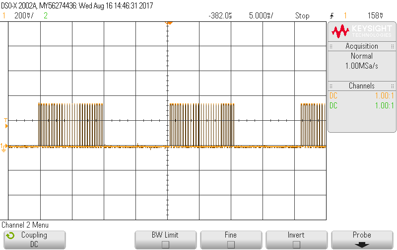
Hi, I am a beginner with MSP430G2553 and CCSV5 coding. I am trying to generate a SPWM by the comparison of a sine wave that I am hard coding and a carrier wave. However according to my code I am unable to obtain switching in the negative cycle.
Is there a particular command/syntax that I can give to level shift my carrier wave such that on comparison of those values negative half of the sine wave is compared as well ?
I have written the aforementioned code.